首页 > ARF476FL > 详情
 Datasheet下载
- 型号: ARF476FL
- 制造商: American Microsemiconductor, Inc.
- 库位|库存: xxxx|xxxx
- 要求:
| 数量阶梯 | 香港交货 | 国内含税 |
| +xxxx | $xxxx | ¥xxxx |
查看当月历史价格
查看今年历史价格
产品参数
| 参数 | 数值 |
| 产品目录 | 分立半导体产品 |
| 描述 | RF FET N CH 500V 10A PSH PUL PR |
| 产品分类 | RF FET |
| 品牌 | Microsemi Power Products Group |
| 数据手册 | http://www.microsemi.com/document-portal/doc_download/122686-arf476fl-c-pdf |
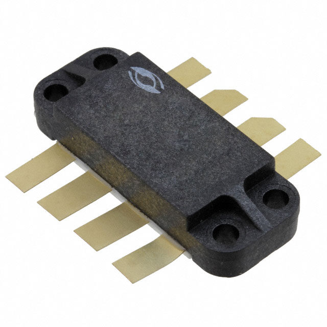
| 产品图片 | |
| 产品型号 | ARF476FL |
| rohs | 无铅 / 符合限制有害物质指令(RoHS)规范要求 |
| 产品系列 | - |
| 供应商器件封装 | * |
| 功率-输出 | 900W |
| 包装 | * |
| 噪声系数 | - |
| 增益 | 16dB |
| 封装/外壳 | * |
| 晶体管类型 | 2 N 沟道(双)共源 |
| 标准包装 | 25 |
| 电压-测试 | 150V |
| 电压-额定 | 500V |
| 电流-测试 | 15mA |
| 频率 | 128MHz |
| 额定电流 | 10A |
Datasheet
PDF Datasheet 数据手册内容提取
Common Source ARF476FL Push-Pull Pair S S S D D S G D ARF476FL D G RF POWER MOSFET S S S G G S N-CHANNEL PUSH - PULL PAIR 165V 450W 150MHz The ARF476FL is a matched pair of RF power transistors in a common source configuration. It is designed for high voltage push-pull or parallel operation in narrow band ISM and MRI power amplifiers up to 150 MHz. • Specified 150 Volt, 128 MHz Characteristics: • High Performance Push-Pull RF Package. • Output Power = 900 Watts Peak • High Voltage Breakdown and Large SOA • Gain = 15dB (Class AB) for Superior Ruggedness. • • Low Thermal Resistance. Efficiency = 50% min • RoHS Compliant * *Pb Free Terminal Finish. MAXIMUM RATINGS All Ratings: T = 25°C unless otherwise specified. C Symbol Parameter ARF476FL UN IT V Drain-Source Voltage 500 DSS Volts VDGO D rain-Gate Voltage 500 I Continuous Drain Current @ T = 25°C (each device) 10 Amps D C V Gate-Source Voltage ±30 Volts GS P Total Device Dissipation @ T = 25°C 910 Watts D C T ,T Operating and Storage Junction Temperature Range -55 to 175 J STG °C T Lead Temperature: 0.063" from Case for 10 Sec. 300 L STATIC ELECTRICAL CHARACTERISTICS (each device) Symbol Characteristic / Test Conditions MIN TYP MAX UNIT BVDSS Drain-Source Breakdown Voltage (VGS = 0V, ID = 250 µA) 500 Volts VDS(ON) On State Drain Voltage 1 (ID(ON) = 5A, VGS = 10V) 2.9 4 Zero Gate Voltage Drain Current (V = V , V = 0V) 100 I DS DSS GS µA DSS Zero Gate Voltage Drain Current (V = 50V, V = 0, T = 125°C) 500 DS GS C IGSS Gate-Source Leakage Current (VGS = ±30V, VDS = 0V) ±100 nA gfs Forward Transconductance (VDS = 15V, ID = 5A) 3 3.6 mhos gfs1/gfs2 Forward Transconductance Match Ratio (VDS = 15V, ID = 5A) 0.9 1.1 VGS(TH) Gate Threshold Voltage (VDS = VGS, ID = 200mA) 2 3.3 4 Volts DVGS(TH) Gate Threshold Voltage Match (VDS = VGS, ID = 200mA) 0.2 THERMAL CHARACTERISTICS Symbol Characteristic MIN TYP MAX UNIT R Junction to Case 0.15 0.165 θJC °C/W R Junction to Sink (Use High Efficiency Thermal Grease and Planar Heat Sink Surface.) 0.30 0.33 θJHS 3 1 0 2 2- CAUTION: These Devices are Sensitive to Electrostatic Discharge. Proper Handling Procedures Should Be Followed. D 1 3 9 4 Microsemi Website - http://www.microsemi.com 50- 0
DYNAMIC CHARACTERISTICS (per section) ARF476FL Symbol Characteristic Test Conditions MIN TYP MAX UNIT C Input Capacitance 780 830 iss V = 0V GS C Output Capacitance V = 50V 125 130 pF oss DS f = 1MHz C Reverse Transfer Capacitance 7 9 rss t Turn-on Delay Time 5.1 10 d(on) V = 15V GS t Rise Time V = 250V 4.1 8 r DD ns t Turn-off Delay Time I = I @ 25°C 12 18 d(off) D D[Cont.] R = 1.6 W t Fall Time G 4.0 7 f FUNCTIONAL CHARACTERISTICS (Push-Pull Configuration) Symbol Characteristic Test Conditions MIN TYP MAX UNIT f = 128 MHz G Common Source Amplifier Power Gain 14 16 dB PS Idq = 15mA V = 150V DD η Drain Efficiency P = 900W 50 55 % out PW = 3ms ψ Electrical Ruggedness VSWR 5:1 No Degradation in Output Power 10% duty cycle 1 Pulse Test: Pulse width < 380 µS, Duty Cycle < 2%. Microsemi Reserves the right to change, without notice, the specifications and information contained herein. Per transistor s ection unless otherwise specified. 30 3000 ES) 25 12V 1000 Ciss R 11V 500 E MP 20 10V pf) Coss NT (A 9V NCE ( 100 RE 15 TA 50 R CI CU 8V PA AIN 10 CA 10 Crss R D 7V , D 5 I 0 1 0 5 10 15 20 25 30 .1 1 10 100 200 V , DRAIN-TO-SOURCE VOLTAGE (VOLTS) V , DRAIN-TO-SOURCE VOLTAGE (VOLTS) DS DS Figure 1, Typical Output Characteristics Figure 2, Typical Capacitance vs. Drain-to-Source Voltage 30 1.10 V > I (ON) x R (ON)MAX. DS D DS 250µSEC. PULSE TEST ES) 25 @ <0.5 % DUTY CYCLE E R G PE TJ = -55°C TA 1.05 M L RENT (A 2105 TJ = +25°C HOLD VOALIZED) 1.00 R SM U ER C RO 2-2013 I, DRAIN D 105 TJ = +125°C TJ = -55°C V, THGS(th)(N 0.95 D 31 00 2 4 6 8 10 0. 90-50 -25 0 25 50 75 100 125 150 050-49 VGFigSu, rGe A3T, ET-yTpOic-aSlO TUraRnCsEfe Vr OCLhTaAraGcEte (rVisOtiLcTsS) Figure 4, TyTpCi,c CaAl TShEr eTsEhMoPldE VRoAlTtaUgReE v (s° CTe)mperature
ARF476FL 0.18 0.16 D = 0.9 0.14 0.12 0.7 0.10 0.5 0.08 Note: 0.06 0.3 DM t1 P 0.04 t2 0.02 0.1 SINGLE PULSE Duty Factor D = t1/t2 0.05 Peak TJ = PDM x ZθJC + TC 0 10-5 10-4 10-3 10-2 10-1 1.0 RECTANGULAR PULSE DURATION (SECONDS) FIGURE 5a, MAXIMUM EFFECTIVE TRANSIENT THERMAL IMPEDANCE, JUNCTION-TO-CASE vs PULSE DURATION 200 OPERATION HERE 100 LIMITED BY RDS (ON) S) E R DC Line Dissipated Power TJ (C) TC (C) MPE (Watts) A 10 T ( 10µs 0.0755 0.0893 XT REN 100µs ZE UR 1ms C 10ms 0.0135F 0.161F N 1 AI 100ms R Z are the external thermal D T =+25°C imEpXTedances: Case to sink, sink to , D TC =+175°C ambient, etc. Set to zero when modeling I SJINGLE PULSE only the case to junction. 0.1 1 10 100 800 V , DRAIN-TO-SOURCE VOLTAGE (VOLTS) Figure 5b, TRANSIENT THERMAL IMPEDANCE MODEL DS Figure 6, Typical Maximum Safe Operating Area Table 1 - Typical Series Equivalent Large Signal Input - Output Impedance Freq. (MHz) Zin (W) gate to gate ZOL (W) drain - drain 30(cid:31) 5.2 -j10(cid:31) 41 -j20 60(cid:31) 1.37 -j5.2 26 -j25 90(cid:31) .53 -j2.6(cid:31) 16 -j23 120(cid:31) .25 -j1.0 10 -j20 150(cid:31) .25 +j0.2 6.7 -j17 Zin - Gate -gate shunted with 25W IDQ = 15mA each side 3 ZOL - Conjugate of optimum load for 600 Watts peak output at Vdd = 150V 201 25% duty cycle and PW = 5ms 2- D 1 3 9 4 0- 5 0
ARF476FL 128MHz Test amplifier + + L3 Po = 900W @150V Vg1 L2 C5 C11 C10 V-dd 3ms pulse 10% Duty Cycle C6 R3 TL3 R1 T2 TL5 J1 T1 C3 T3 TL1 C7 C2 L1 C1 J2 C8 TL2 C4 R2 R4 C9 TL4 TL6 C1 25pF poly trimmer DUT C2 750pF ATC 700B Vg2 C3-4 2200pF NPO 500V chip R1-2 3.1W : 3 parallel 22W 1W 2512 SMT C5-10 10nF 500V chip R3-4 2.2kW 1/4W axial C11 1000uF 250V electroytic T1 1:1 balun 50W coax on Fair-Rite 2843000102 core L1 30nH 1.5t #18 enam .375" dia T2 4:1 25W coax on 2843000102 Fair-Rite balun core L2 680nH 12t #24 enam .312" dia T3 1:1 coax balun RG-303 on 2861006802 Fair-Rite core L3 2t #20 on Fair-Rite 2643006302 bead, ~ 2uH TL1-2 Printed line L= 0.75" w=.23" TL3-6 Printed line L= 0.65" w=.23" 0.23" wide stripline on FR-4 board is ~ 30W Zo Peak Output Power vs. Vdd and Duty Cycle 900 1.2 Notes: 800 The value of L1 must be adjusted as the supply voltage is Max 1 changed to maintain resonance in the output circuit. At 700 Duty Cycle 128MHz its value changes from approximately 40nH at 100V to 30nH at 150V. 600 0.8 500 With the 50W drain-to-drain load, the duty cycle above Po Watts 0.6 100V must be reduced to insure power dissipation is 400 within the limits of the device. Maximum pulse length should be 100mS or less. See transient thermal 300 0.4 impedance, figure 5. 200 0.2 100 0 0 80 100 120 140 160 Drain Supply Voltage Vdd 00 00 00 Thermal Considerations and Package Mounting: 1 1 1 . . . The rated power dissipation is only available when the package .325 +/- .010 1.000 mounting surface is at 25°C and the junction temperature is 175°C. The .41 2p5lsR .080 .41 2p5lsdia thermal resistance between junctions and case mounting surface is 0.16 °C/W. When installed, an additional thermal impedance of 0.15°C/W between the package base and the mounting surface is typical. Insure that the mounting surface is smooth and flat. Thermal joint compound must be .570 used to reduce the effects of small surface irregularities. Use the minimum ARF476FL .320 amount necessary to coat the surface. The heatsink should incorporate a copper heat spreader to obtain best results. The package design clamps the ceramic base to the heatsink. A clamped joint maintains the required mounting pressure while allowing for 1.250 thermal expansion of both the base and the heat sink. Four 4-40 (M3) .325 screws provide the required mounting force. T = 3-4 in-lb (0.34 - 0.45 N-m). .150 .175 .175 .150 HAZARDOUS MATERIAL WARNING The white ceramic portion of the device between leads .200 and mounting surface is beryllium oxide, BeO. Beryllium 13 .300 oxide dust is toxic when inhaled. Care must be taken 20 .005 .040 during handling and mounting to avoid damage to this D 2- area. These devices must never be thrown away with 1 1.500 general industrial or domestic waste. BeO substrate 3 weight: 1.3g. Percentage of total module weight which is 9 4 BeO: 23%. 0- 5 0