首页 > APT35GP120BG > 详情
 Datasheet下载
- 型号: APT35GP120BG
- 制造商: American Microsemiconductor, Inc.
- 库位|库存: xxxx|xxxx
- 要求:
| 数量阶梯 | 香港交货 | 国内含税 |
| +xxxx | $xxxx | ¥xxxx |
查看当月历史价格
查看今年历史价格
产品参数
| 参数 | 数值 |
| 25°C时Td(开/关)值 | 16ns/94ns |
| 产品目录 | 分立半导体产品 |
| Current-CollectorPulsed(Icm) | 140A |
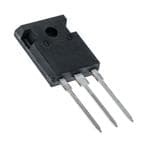
| 描述 | IGBT 1200V 96A 543W TO247 |
| 产品分类 | IGBT - 单路 |
| GateCharge | 150nC |
| IGBT类型 | PT |
| 品牌 | Microsemi Power Products Group |
| 数据手册 | http://www.microsemi.com/document-portal/doc_download/6969-apt35gp120b-g-e-pdfhttp://www2.microsemi.com/document-portal/doc_download/14813-power-products-group-ppg-catalog |
| 产品图片 |  |
| 产品型号 | APT35GP120BG |
| rohs | 无铅 / 符合限制有害物质指令(RoHS)规范要求 |
| 产品系列 | POWER MOS 7® |
| SwitchingEnergy | 750µJ (开), 680µJ (关) |
| TestCondition | 600V, 35A, 5 欧姆, 15V |
| 不同 Vge、Ic时的 Vce(on) | 3.9V @ 15V,35A |
| 产品目录绘图 |  |
| 产品目录页面 | 点击此处下载产品Datasheet |
| 供应商器件封装 | TO-247 [B] |
| 其它名称 | APT35GP120BGMI APT35GP120BGMI-ND |
| 功率-最大值 | 543W |
| 包装 | 管件 |
| 反向恢复时间(trr) | - |
| 安装类型 | 通孔 |
| 封装/外壳 | TO-247-3 |
| 标准包装 | 30 |
| 电压-集射极击穿(最大值) | 1200V |
| 电流-集电极(Ic)(最大值) | 96A |
| 输入类型 | 标准 |
Datasheet
PDF Datasheet 数据手册内容提取
APT35GP120B APT35GP120BG *G Denotes RoHS Compliant, Pb Free Terminal Finish. POWER MOS 7® IGBT TO-247 The POWER MOS 7® IGBT is a new generation of high voltage power IGBTs. Using Punch Through Technology this IGBT is ideal for many high frequency, high voltage switching applications and has been optimized for high frequency G switchmode power supplies. C E C •Low Conduction Loss •100 kHz operation @ 800V, 14A •Low Gate Charge •50 kHz operation @ 800V, 25A G •Ultrafast Tail Current shutoff •RBSOA rated E MAXIMUM RATINGS All Ratings: T = 25°C unless otherwise specified. C Symbol Parameter APT35GP120B(G) UNIT V Collector-Emitter Voltage 1200 CES VGE Gate-Emitter Voltage ±20 Volts V Gate-Emitter Voltage Transient ±30 GEM IC1 Continuous Collector Current @ TC = 25°C 96 IC2 Continuous Collector Current @ TC = 110°C 46 Amps ICM Pulsed Collector Current 1 @ TC = 25°C 140 RBSOA Reverse Bias Safe Operating Area @ T = 150°C 140A @ 960V J PD Total Power Dissipation 543 Watts T ,T Operating and Storage Junction Temperature Range -55 to 150 J STG °C TL Max. Lead Temp. for Soldering: 0.063" from Case for 10 Sec. 300 STATIC ELECTRICAL CHARACTERISTICS Symbol Characteristic / Test Conditions MIN TYP MAX UNIT BV Collector-Emitter Breakdown Voltage (V = 0V, I = 250µA) 1200 CES GE C V Gate Threshold Voltage (V = V , I = 1mA, T = 25°C) 3 4.5 6 GE(TH) CE GE C j Volts Collector-Emitter On Voltage (V = 15V, I = 35A, T = 25°C) 3.3 3.9 GE C j V CE(ON) Collector-Emitter On Voltage (V = 15V, I = 35A, T = 125°C) 3 GE C j Collector Cut-off Current (V = 1200V, V = 0V, T = 25°C) 2 250 CE GE j I µA CES Collector Cut-off Current (V = 1200V, V = 0V, T = 125°C) 2 2500 CE GE j 6 0 IGES Gate-Emitter Leakage Current (VGE = ±20V) ±100 nA 2-20 1 E CAUTION: These Devices are Sensitive to Electrostatic Discharge. Proper Handling Procedures Should Be Followed. v e R 6 Microsemi Website - http://www.microsemi.com 40 7 0- 5 0
DYNAMIC CHARACTERISTICS APT35GP120B(G) Symbol Characteristic Test Conditions MIN TYP MAX UNIT Cies Input Capacitance Capacitance 3240 C Output Capacitance V = 0V, V = 25V 248 pF oes GE CE C Reverse Transfer Capacitance f = 1 MHz 31 res VGEP Gate-to-Emitter Plateau Voltage Gate Charge 7.5 V Qg Total Gate Charge 3 VGE = 15V 150 Qge Gate-Emitter Charge VCE = 600V 21 nC I = 35A Qgc Gate-Collector ("Miller") Charge C 62 RBSOA Reverse Bias Safe Operating Area T = 150°C, R = 5Ω, V = 140 A J G GE 15V, L = 100µH,V = 960V CE t Turn-on Delay Time Inductive Switching (25°C) 16 d(on) tr Current Rise Time VCC = 600V 20 ns V = 15V td(off) Turn-off Delay Time GE 94 I = 35A t Current Fall Time C 40 f R = 5Ω E Turn-on Switching Energy 4 G 750 on1 T = +25°C Eon2 Turn-on Switching Energy (Diode) 5 J 1305 µJ E Turn-off Switching Energy 6 680 off t Turn-on Delay Time Inductive Switching (125°C) 16 d(on) tr Current Rise Time VCC = 600V 20 V = 15V ns td(off) Turn-off Delay Time GE 147 I = 35A t Current Fall Time C 75 f R = 5Ω E Turn-on Switching Energy 4 G 750 on1 T = +125°C Eon2 Turn-on Switching Energy (Diode) 5 J 2132 µJ E Turn-off Switching Energy 6 1744 off THERMAL AND MECHANICAL CHARACTERISTICS Symbol Characteristic MIN TYP MAX UNIT R Junction to Case (IGBT) .23 ΘJC °C/W R Junction to Case (DIODE) N/A ΘJC W Package Weight 5.90 gm T 1 Repetitive Rating: Pulse width limited by maximum junction temperature. 2 For Combi devices, I includes both IGBT and FRED leakages ces 3 See MIL-STD-750 Method 3471. 4 E is the clamped inductive turn-on-energy of the IGBT only, without the effect of a commutating diode reverse recovery current on1 adding to the IGBT turn-on loss. (See Figure 24.) 5 E is the clamped inductive turn-on energy that includes a commutating diode reverse recovery current in the IGBT turn-on switching on2 loss. (See Figures 21, 22.) 6 E is the clamped inductive turn-off energy measured in accordance with JEDEC standard JESD24-1. (See Figures 21, 23.) off Microsemi reserves the right to change, without notice, the specifications and information contained herein. 6 0 0 2 2- 1 E v e R 6 0 4 7 0- 5 0
TYPICAL PERFORMANCE CURVES APT35GP120B(G) 80 80 VGE = 15V. VGE = 10V. 250µs PULSE TEST 250µs PULSE TEST 70 <0.5 % DUTY CYCLE 70 <0.5 % DUTY CYCLE A) A) T ( 60 T ( 60 N N E E RR 50 RR 50 U U C C OR 40 TC=25°C OR 40 TC=25°C T T C 30 C 30 LE TC=125°C LE L L O 20 O 20 TC=125°C C C , C , C I 10 I 10 0 0 0 1 2 3 4 5 0 1 2 3 4 5 V , COLLECTER-TO-EMITTER VOLTAGE (V) V , COLLECTER-TO-EMITTER VOLTAGE (V) CE CE FIGURE 1, Output Characteristics(V = 15V) FIGURE 2, Output Characteristics (V = 10V) GE GE 120 16 250µs PULSE TEST IC = 35A A) 100 <0.5 % DUTY CYCLE GE (V) 14 TJ = 25°C ENT ( 80 OLTA 12 VCE= 240V URR R V 10 VCE= 600V OR C 60 MITTE 8 VCE= 960V T E COLLEC 40 TJ = T1J2 5=° 2C5°C ATE-TO- 64 I, C 20 , GE 2 G TJ = -55°C V 0 0 0 1 2 3 4 5 6 7 8 9 10 0 20 40 60 80 100 120 140 160 V , GATE-TO-EMITTER VOLTAGE (V) GATE CHARGE (nC) GE FIGURE 3, Transfer Characteristics FIGURE 4, Gate Charge OLTAGE (V) 65 IC= 70A 2 <500.µ5s %TPJ UD =LU S2T5EY° CT CE.YSCTLE OLTAGE (V) 4.554 2 <500.µ5 s V% PG UDELU =ST E1Y 5 TCVEY.SCTLE IC=70A R V 4 R V 3.5 IC= 35A E E TT IC= 35A TT 3 EMI 3 EMI 2.5 TO- IC=17.5A TO- 2 IC= 17.5A TOR- 2 TOR- 1.5 C C OLLE 1 OLLE 1 C C 0.5 , CE 0 , CE 0 V 6 8 10 12 14 16 V 0 25 50 75 100 125 V , GATE-TO-EMITTER VOLTAGE (V) T, Junction Temperature (°C) GE J FIGURE 5, On State Voltage vs Gate-to- Emitter Voltage FIGURE 6, On State Voltage vs Junction Temperature N W 1.2 140 O D AK 1.15 A) 120 R BREZED) 1.1 RENT( 100 O-EMITTENORMALI 1.10.50 TOR CUR 80 COLLECTOR-TVOLTAGE ( 000...998505 DC COLLECC, 642000 E 12-2006 BV, CES 0.8-50 -T2J5, JUN0CTIO25N TE5M0PER75ATU1R00E (°1C2)5 150 I 0-50 -25TC, C0ASE2 5TEM5P0ERA7T5UR1E0 0(°C1)25 150 06 Rev FIGURE 7, Breakdown Voltage vs. Junction Temperature FIGURE 8, DC Collector Current vs Case Temperature 4 7 0- 5 0
APT35GP120B(G) 35 180 s) 30 ns) 160 E (n VGE= 10V ME ( 140 VGE =15V,TJ=125°C Y TIM 25 AY TI 120 VGE =10V,TJ=125°C ELA 20 VGE= 15V DEL 100 VGE =15V,TJ=25°C N D FF O 15 O 80 TURN- 10 TURN- 60 VGE =10V,TJ=25°C t, d(ON) 5 VTRL JCG= E = =1 = 025 056Ω °0µC0H,V TJ =125°C t , d(OFF) 4200 VRL GC= E =1 = 05 06Ω 0µ0HV 0 0 10 20 30 40 50 60 70 10 20 30 40 50 60 70 I , COLLECTOR TO EMITTER CURRENT (A) I , COLLECTOR TO EMITTER CURRENT (A) CE CE FIGURE 9, Turn-On Delay Time vs Collector Current FIGURE 10, Turn-Off Delay Time vs Collector Current 140 100 RG = 5Ω, L = 100µH, VCE = 600V 90 TJ = 125°C, VGE = 10V or 15V 120 80 s) 100 TJ = 25 or125°C,VGE = 10V s) 70 n n E ( 80 E ( 60 M M TI TI 50 RISE 60 FALL 40 tr, 40 tf, 30 TJ = 25°C, VGE = 10V or 15V 20 20 10 TJ = 25 or 125°C,VGE =10V RG = 5Ω, L = 100µH, VCE = 600V 0 0 10 20 30 40 50 60 70 10 20 30 40 50 60 70 I , COLLECTOR TO EMITTER CURRENT (A) I , COLLECTOR TO EMITTER CURRENT (A) CE CE FIGURE 11, Current Rise Time vs Collector Current FIGURE 12, Current Fall Time vs Collector Current 5000 4000 S (µJ) 4000 VRCGE = = 5 6Ω00V TJ=125°C,VGE=15V SS (µJ) VRCGE = = 5 6Ω00V N ENERGY LOS 3000 TJ=125°C,VGE=10V F ENERGY LO 32000000 TJ = 125°C, VGE = 10V or 15V RN O 2000 N OF TU TJ= 25°C,VGE=15V UR 1000 E, ON2 1000 TJ= 25°C,VGE=10V E, TOFF TJ = 25°C, VGE = 10V or 15V 0 0 10 20 30 40 50 60 70 10 20 30 40 50 60 70 I , COLLECTOR TO EMITTER CURRENT (A) I , COLLECTOR TO EMITTER CURRENT (A) CE CE FIGURE 13, Turn-On Energy Loss vs Collector Current FIGURE 14, Turn Off Energy Loss vs Collector Current 8000 5000 µJ) 7000 VVTJCG =EE 1==2 56+°01C05VV Eon2 70A µJ) VVRCGGEE = == 5 6+Ω0105VV Eon2 70A S ( S ( 4000 E 6000 E S S S S O O L 5000 L RGY 4000 Eoff 70A RGY 3000 Eoff70A NE NE Eon2 35A ev E 12-2006 SWITCHING E 3210000000000 EEoonn22 3157A.5A EoEff o1ff7 3.55AA SWITCHING E 210000000 Eoff 35A Eoff 17.5A Eon2 17.5A R 06 0 RG1, 0GATE R20ESISTA3N0CE (OH4M0S) 50 0 TJ, J2U5NCTIO5N0 TEMPE7R5ATUR1E0 (0°C) 125 4 FIGURE 15, Switching Energy Losses vs. Gate Resistance FIGURE 16, Switching Energy Losses vs Junction Temperature 7 0- 5 0
TYPICAL PERFORMANCE CURVES APT35GP120B(G) 10,000 160 5,000 Cies 140 F) 120 NCE (P1,050000 ENT (A) 100 CITA Coes URR 80 A C CAP 100 OR 60 C, 50 CT 40 E L Cres OL 20 C 10 I, C 0 0 10 20 30 40 50 0 100200300 400500600700 8009001000 VCE, COLLECTOR-TO-EMITTER VOLTAGE (VOLTS) VCE, COLLECTOR TO EMITTER VOLTAGE Figure 17, Capacitance vs Collector-To-Emitter Voltage Figure 18, Reverse Bias Safe Operating Area 0.25 0.9 W) 0.20 C/ E (° 0.7 C N 0.15 A D PE 0.5 M L I 0.10 Note: A ERM 0.3 PDM t1 H , TJCθ 0.05 0.1 Duty Factort 2 D = t1/t2 Z 0.05 SINGLE PULSE Peak TJ = PDM x ZθJC + TC 0 10-5 10-4 10-3 10-2 10-1 1.0 RECTANGULAR PULSE DURATION (SECONDS) Figure 19, Maximum Effective Transient Thermal Impedance, Junction-To-Case vs Pulse Duration T ((cid:31)C) T ((cid:31)C) J C Z are the external thermal 0.0896 0.140 T imEpXTedances: Case to sink, Dissipated Power EX sink to ambient, etc. Set to (Watts) Z zero when modeling only 0.0108 0.228 the case to junction. FIGURE 19B, TRANSIENT THERMAL IMPEDANCE MODEL 180 z) H Y (k 100 C N E U Q 50 E F =min(f ,f ) R max max1 max2 F ATING fmax1=td(on)+tr0+.0t5d(off)+tf 006 F, OPERMAX 10710TTDVRJCCG = =E = =5 = 0157 2 5%8Ω25°0°0C0CV 30 40 50 60 70 fPmdiasxs2==TEPRJdo−iθsnsJ2TC−+CPEcoonfdf 6 Rev E 12-2 F i g u r e I2C0, ,C OOpLeLrEaCtinTgO R F rCeUqRueRnEcNyT v (sA )Collector 0-740 Current 5 0
APT35GP120B(G) Gate Voltage APT30DF120 10% T = 125 (cid:31)C t J d(on) t VCC IC VCE r 90% Collector Current 5% 10% 5 % A Collector Voltage D.U.T. Switching Energy Figure 21, Inductive Switching Test Circuit Figure 22, Turn-on Switching Waveforms and Definitions 90% VTEST t *DRIVER SAME TYPE AS D.U.T. d(off) Gate Voltage T = 125 (cid:31)C J 90% A t f Collector Voltage VCE IC 10% 100uH 0 VCLAMP B Collector Current Switching A Energy DRIVER* D.U.T. Figure 23, Turn-off Switching Waveforms and Definitions Figure 24, E Test Circuit ON1 T0-247 Package Outline e1 SAC: Tin, Silver, Copper 4.69 (.185)(cid:31) 5.31 (.209) 15.49 (.610)(cid:31) 1.49 (.059)(cid:31) 16.26 (.640) 2.49 (.098) 5.38 (.212)(cid:31) 6.15 (.242) BSC 6.20 (.244) or 20.80 (.819)(cid:31) ct 21.46 (.845) e oll 3.50 (.138)(cid:31) C 3.81 (.150) 2.87 (.113)(cid:31) 4.50 (.177) Max. 3.12 (.123) 0.40 (.016)(cid:31) 1.65 (.065)(cid:31) 0.79 (.031) 19.81 (.780)(cid:31) 2.13 (.084) 20.32 (.800) 1.01 (.040)(cid:31) Gate 006 1.40 (.055) Collector 2 2- Emitter 1 E ev 22..2519 ((..018072))(cid:31) 5.45 (.215) BSC R 06 Dimensions in Millimeters 2a-nPdlc s(I.nches) 4 0-7 Microsemi’s products are covered by one or more of U.S.patents 4,895,810 5,045,903 5,089,434 5,182,234 5,019,5225,262,336 6,503,786 5 5,256,583 4,748,103 5,283,202 5,231,474 5,434,095 5,528,058 and foreign patents. US and Foreign patents pending. All Rights Reserved. 0
Mouser Electronics Authorized Distributor Click to View Pricing, Inventory, Delivery & Lifecycle Information: M icrosemi: APT35GP120BG