ICGOO在线商城 > 集成电路(IC) > PMIC - 稳压器 - DC DC 开关稳压器 > AP1509-12SG-13

 Datasheet下载
- 型号: AP1509-12SG-13
- 制造商: Diodes Inc.
- 库位|库存: xxxx|xxxx
- 要求:
| 数量阶梯 | 香港交货 | 国内含税 |
| +xxxx | $xxxx | ¥xxxx |
查看当月历史价格
查看今年历史价格
AP1509-12SG-13产品简介:
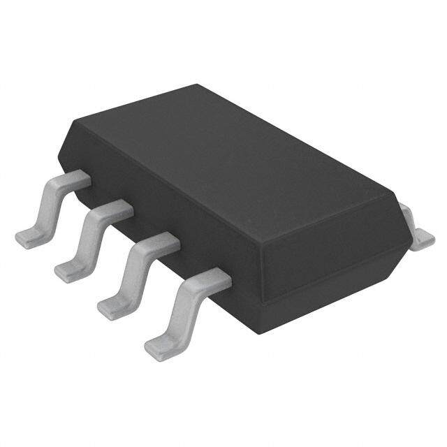
ICGOO电子元器件商城为您提供AP1509-12SG-13由Diodes Inc.设计生产,在icgoo商城现货销售,并且可以通过原厂、代理商等渠道进行代购。 AP1509-12SG-13价格参考。Diodes Inc.AP1509-12SG-13封装/规格:PMIC - 稳压器 - DC DC 开关稳压器, 固定 降压 开关稳压器 IC 正 12V 1 输出 2A 8-SOIC(0.154",3.90mm 宽)。您可以下载AP1509-12SG-13参考资料、Datasheet数据手册功能说明书,资料中有AP1509-12SG-13 详细功能的应用电路图电压和使用方法及教程。
Diodes Incorporated的AP1509-12SG-13是一款PMIC(电源管理集成电路)中的DC-DC开关稳压器,广泛应用于需要高效、稳定电压转换的场景。以下是其主要应用场景:

1. 消费电子设备:该型号适合用于智能手机、平板电脑、可穿戴设备等便携式电子产品中,为系统提供稳定的电源供应。其高效的转换能力和小尺寸设计非常适合对空间和功耗敏感的应用。

2. 物联网(IoT)设备:在低功耗需求的IoT设备中,如传感器节点、智能家居设备等,AP1509-12SG-13能够提供可靠的电源管理解决方案,确保设备长时间运行。

3. 通信设备:适用于路由器、交换机、网关等通信设备中,为内部电路提供所需的电压转换,支持设备的正常运行。

4. 工业自动化:在工业控制模块、数据采集系统等场景中,这款稳压器可以为各种传感器和执行器提供稳定的电源,满足工业环境下的高可靠性要求。

5. 汽车电子:虽然具体车规认证需进一步确认,但在非关键车载应用中(如信息娱乐系统、导航设备等),AP1509-12SG-13也可以发挥作用,提供高效的电压转换。

6. 医疗设备:在便携式医疗设备(如血压计、血糖仪等)中,该型号的低功耗特性和高效率有助于延长电池寿命,同时保持设备性能稳定。

总结来说,AP1509-12SG-13凭借其高效能、小体积和稳定性,适用于多种需要低压差、高效率电源转换的场景,尤其适合便携式和低功耗应用领域。
| 参数 | 数值 |
| 产品目录 | 集成电路 (IC) |
| 描述 | IC REG BUCK 12V 2A 8SOIC |
| 产品分类 | |
| 品牌 | Diodes Incorporated |
| 数据手册 | |
| 产品图片 |
|
| 产品型号 | AP1509-12SG-13 |
| PWM类型 | 电压模式 |
| rohs | 无铅 / 符合限制有害物质指令(RoHS)规范要求 |
| RoHS指令信息 | http://diodes.com/download/4349 |
| 产品系列 | - |
| 供应商器件封装 | 8-SOP |
| 其它名称 | AP1509-12SGDIDKR |
| 包装 | Digi-Reel® |
| 同步整流器 | 无 |
| 安装类型 | 表面贴装 |
| 封装/外壳 | 8-SOIC(0.154",3.90mm 宽) |
| 工作温度 | -20°C ~ 85°C |
| 标准包装 | 1 |
| 电压-输入 | 4.5 V ~ 22 V |
| 电压-输出 | 12V |
| 电流-输出 | 2A |
| 类型 | 降压(降压) |
| 输出数 | 1 |
| 输出类型 | 固定 |
| 频率-开关 | 150kHz |


- 商务部:美国ITC正式对集成电路等产品启动337调查
- 曝三星4nm工艺存在良率问题 高通将骁龙8 Gen1或转产台积电
- 太阳诱电将投资9.5亿元在常州建新厂生产MLCC 预计2023年完工
- 英特尔发布欧洲新工厂建设计划 深化IDM 2.0 战略
- 台积电先进制程称霸业界 有大客户加持明年业绩稳了
- 达到5530亿美元!SIA预计今年全球半导体销售额将创下新高
- 英特尔拟将自动驾驶子公司Mobileye上市 估值或超500亿美元
- 三星加码芯片和SET,合并消费电子和移动部门,撤换高东真等 CEO
- 三星电子宣布重大人事变动 还合并消费电子和移动部门
- 海关总署:前11个月进口集成电路产品价值2.52万亿元 增长14.8%


PDF Datasheet 数据手册内容提取
AP1509 150kHz, 2A PWM BUCK DC-DC CONVERTER Description Pin Assignments The AP1509 series are monolithic ICs designed for a step-down DC-DC converter and have the ability of driving a 2A load without an additional transistor, which saves board space. (Top View) The external shutdown function can be controlled by logic level and VIN 1 8 GND then go into standby mode. The internal compensation makes Output 2 7 GND feedback control have good line and load regulation without external AP1509 design. Regarding protected function, thermal shutdown prevents FB 3 6 GND overtemperature operating from damage, and current limit works SD 4 5 GND against overcurrent operating of the output switch. If current limit function occurs, and VFB is below 0.5V, the switching frequency is SOP-8L reduced. The AP1509 series operates at a switching frequency of 150kHz thus allowing smaller-sized filter components than what is required with lower frequency switching regulators. Other features include a guaranteed +4% tolerance on output voltage under specified input voltage and output load conditions, and +15% on the oscillator frequency. The output version included fixed 3.3V, 5V, 12V, and an adjustable type. The chips are available in a standard 8-lead SO-8 package. Features Applications • Output Voltage: 3.3V, 5V, 12V, and Adjustable Output Version • Simple High-Efficiency Step-Down Regulator • Adjustable Version Output Voltage Range of 1.23V to 18V+4% • On-Card Switching Regulators • 150kHz +15% Fixed Switching Frequency • Positive to Negative Converter • Voltage Mode Non-Synchronous PWM Control • Thermal-Shutdown and Current-Limit Protection • ON/OFF Shutdown Control Input • Operating Voltage up to 22V • Output Load Current: 2A • Low Power Standby Mode • Built-in Switching Transistor On Chip • Totally Lead-Free & Fully RoHS Compliant (Note 1 & 2) • Halogen and Antimony Free. “Green” Device (Note 3) Notes: 1. No purposely added lead. Fully EU Directive 2002/95/EC (RoHS), 2011/65/EU (RoHS 2) & 2015/863/EU (RoHS 3) compliant. 2. See https://www.diodes.com/quality/lead-free/ for more information about Diodes Incorporated’s definitions of Halogen- and Antimony-free, "Green" and Lead-free. 3. Halogen- and Antimony-free "Green” products are defined as those which contain <900ppm bromine, <900ppm chlorine (<1500ppm total Br + Cl) and <1000ppm antimony compounds. AP1509 1 of 12 October 2018 Document number: DS31016 Rev. 5 - 2 www.diodes.com © Diodes Incorporated
AP1509 Typical Application Circuit (1) Fixed Type Circuit FB 12V 3 L1 3.3V/2A DC Input AP1509- Output 47uH Output Load 1 2 VIN 33 Inductor 4 5 6 7 8 CIN SD GNDGNDGNDGND D1 Co Capacitor Schottky Diode Capacitor (2) Adjustable Type Circuit R2 1K R1 1K FB 12V 3 L1 2.5V/2A DC Input Output 39uH Output Load 1 AP1509 2 V Inductor IN 4 5 6 7 8 D1 CIN SD GND GND GND GND Co Schottky Capacitor Capacitor Diode R1 VOUT = VFB × (1 + ) R2 VFB = 1.23V R2 = 1K ~ 3K (3) Delay Start Circuit R2 1K R1 1K FB 12V 3 L1 2.5V/2A DC Input V Output 39uH Output Load IN 1 AP1509 2 Inductor C DELAY 4 5 6 7 8 0.1uF D1 SD GND GND GND GND Co Schottky CIN RDELAY Diode Capacitor Capacitor 10K AP1509 2 of 12 October 2018 Document number: DS31016 Rev. 5 - 2 www.diodes.com © Diodes Incorporated
AP1509 Pin Descriptions Pin Name Description VIN Operating Voltage Input Output Switching Output GND Ground FB Output Voltage Feedback Control SD ON/OFF Shutdown Functional Block Diagram SD V IN 200mV 220mV Current 1.235V 2.5V Start Source Reference Regulator up bias + Comp _ _ Comp + + Frequecy FB _Amp cosmatpioenn- C+_omp dPrirvee-r Sw2iAtch Output 150kH z Thermal OSC. Shutdown GND AP1509 3 of 12 October 2018 Document number: DS31016 Rev. 5 - 2 www.diodes.com © Diodes Incorporated
AP1509 Absolute Maximum Ratings Symbol Parameter Rating Unit ESD HBM Human Body Model ESD Protection KV 2 ESD MM Machine Model ESD Protection 200 V VIN Supply Voltage +24 V VSD ON/OFF Pin Input Voltage -0.3 to +18 V VFB Feedback Pin Voltage -0.3 to +18 V VOUT Output Voltage to Ground -1 V PD Power Dissipation Internally Limited W TST Storage Temperature -65 to +150 °C TJ Operating Junction Temperature -40 to +125 °C Recommended Operating Conditions Symbol Parameter Min Max Unit IOUT Output Current 0 2 A VOP Operating Voltage 4.5 22 V TA Operating Ambient Temperature -20 85 °C AP1509 4 of 12 October 2018 Document number: DS31016 Rev. 5 - 2 www.diodes.com © Diodes Incorporated
AP1509 Electrical Characteristics Unless otherwise specified, VIN = 12V for 3.3V, 5V, adjustable version, and VIN = 18V for the 12V version. ILOAD = 0.5A Specifications with boldface type are for full operating temperature range, the other type are for TJ = 25°C. Symbol Parameter Conditions Min Typ. Max Unit IFB Feedback Bias Current V(AFdBj u=s 1ta.3bVle Version Only) — -10 --15000 nA 127 150 173 FOSC Oscillator Frequency — 110 173 kHz Oscillator Frequency of Short Circuit When Current Limit Occurred and FSCP Protect VFB < 0.5V, Ta = 25°C 10 30 50 kHz IOUT = 2A 1.4 VSAT Saturation Voltage No Outside Circuit — 1.25 1.5 V VFB = 0V Force Driver On DC Max. Duty Cycle (ON) VFB = 0V Force Driver On — 100 — % Min. Duty Cycle (OFF) VFB = 12V Force Driver Off — 0 — Peak Current ICL Current Limit No Outside Circuit 3 — — A VFB = 0V Force Driver On No Outside Circuit Output = 0 — — -200 µA IL Output Leakage Current VFB = 12V Force Driver Off Output = -1 VIN = 22V — -5 mA IQ Quiescent Current VFB = 12V Force Driver Off — 5 10 mA ON/OFF pin = 5V 150 ISTBY Standby Quiescent Current VIN = 22V — 70 200 µA VIL Low (Regulator ON) — 0.6 ON/OFF Pin Logic Input Threshold 1.3 V VIH Voltage High (Regulator OFF) 2.0 — IH ON/OFF Pin Logic Input Current VLOGIC = 2.5V (OFF) — — -0.01 µA IL ON/OFF Pin Input Current VLOGIC = 0.5V (ON) — -0.1 -1 ϴJA Thermal Resistance SO-8 Junction to Case — 15 — °C/W Thermal Resistance ϴJC with a Copper Area of Approximately SO-8 Junction to Ambient — 70 — °C/W 2 3in VFB Output 40..52VA << VILIONA <D 2<2 2VA 1.193 1.23 1.267 V Feedback 1.18 1.28 AP1509 - ADJ VOUT Programmed for 3V Ƞ Efficiency VIN = 12V, ILOAD=2A 76 76 — % VOUT Output Voltage 4.75V < VIN < 22V 3.168 3.3 3.432 V AP1509 - 3.3V 0.2A < ILOAD < 2A 3.135 3.465 Ƞ Efficiency VIN = 12V, 78 78 — % ILOAD = 2A VOUT Output Voltage 7V < VIN < 22V 4.8 5 5.2 V AP1509 - 5V 0.2A < ILOAD < 2A 4.75 5.25 Ƞ Efficiency VIN = 12V, 83 83 — % ILOAD = 2A VOUT Output Voltage 15V < VIN < 22V 11.52 12 12.48 V AP1509 - 12V 0.2A < ILOAD < 2A 11.4 12.6 Ƞ Efficiency VIN = 15V, 90 90 — % ILOAD = 2A AP1509 5 of 12 October 2018 Document number: DS31016 Rev. 5 - 2 www.diodes.com © Diodes Incorporated
AP1509 Typical Performance Characteristics AP1509 Efficiency vs. Temperature AP1509 Efficiency vs. Temperature (VIN = 12V, VOUT = 5V, Io = 2A) (VIN = 12V, VOUT = 3.3V, Io = 2A) 86 81 85 80 84 83 79 %) 82 78 ncy ( 8801 y (%) 77 Efficie 777789 Efficienc 7756 74 76 75 73 -50 -30 -10 10 30 50 70 90 110130150 -50 -30 -10 10 30 50 70 90 110 130 150 Temperature (T ) (°C) A Temperature (T ) (°C) A AP1509 Saturation Voltage vs. Temperature AP1509 Switch Current Limit vs. Temperature (VIN = 12V, VFB = 0V, VSD = 0) (VIN = 12V, VFB = 0V) 1.4 5.5 1.3 A) e (V) 1.2 2A Limit ( 5 ag 1.1 nt 4.5 n Volt 1 0.5A1A Curre 4 uratio 00..89 witch 3.5 at S S 0.7 3 -50 -25 0 25 50 75 100 125 -50 -30 -10 10 30 50 70 90 Temperature (TA) (°C) Temperature (TA) (°C) AP1509 Supply Current vs. Temperature (VIN = 12V, No Load, Von/off = 0V (Switch ON) ,Von/off = 5V (Switch OFF)) 15 60 14 13 55 A) 12 uA) ent (m 1101 rrent ( 4550 Switch OFF y Curr 789 Switch ON ply Cu 40 Suppl 56 Sup 3305 -50 -30 -10 10 30 50 70 90 110 130 150 -50 -30 -10 10 30 50 70 90 110 130 150 Temperature (TA) (°C) Temperature (TA) (°C) AP1509 6 of 12 October 2018 Document number: DS31016 Rev. 5 - 2 www.diodes.com © Diodes Incorporated
AP1509 Typical Performance Characteristics (continued) AP1509 Threshold Voltage vs. Temperature AP1509 ON/OFF Current vs. ON/OFF Voltage (VIN = 12V, Io = 100mA) (VIN = 12V) 1.7 10 1.6 0 -10 1.5 V) A)-20 e (1.4 (n-30 Voltag11..23 urrent --5400 d C-60 ol1.1 F h F-70 s 1 O Thre0.9 ON/--9800 0.8 -100 -50 -30 -10 10 30 50 70 90 110 130 150 0 3 6 9 12 15 18 21 Temperature (TA) (°C) ON/OFF Voltage (V) AP1509 Frequency vs. Temperature AP1509 Feedback Current vs. Temperature (VIN = 12V, Io = 500mA, VOUT = 5V) (VIN = 12V, VOUT = 5V, Vfb = 1.3V) 170 10 165 A) 0 KHz)160 ent (n -10 y (155 urr -20 c C uen150 ack -30 q b e d Fr145 ee -40 F 140 -50 -50 -30 -10 10 30 50 70 90 110 130 150 -50 -30 -10 10 30 50 70 90 110 130 150 Temperature (TA) (°C) Temperature (TA) (°C) AP1509 Output Voltage vs. Temperature (VIN = 12V, Io = 2A) 3.5 3.45 3.4 3.35 3.3 V)3.25 ( T 3.2 U O3.15 V 3.1 3.05 3 2.95 2.9 -40 -20 0 20 40 60 80 100 120 140 160 Temperature (TA) (°C) AP1509 7 of 12 October 2018 Document number: DS31016 Rev. 5 - 2 www.diodes.com © Diodes Incorporated
AP1509 Typical Performance Characteristics (continued) Header Frequency vs. Temperature Feedback Voltage vs. Temperature (VIN = 15V, VOUT = 5V) 1000 1.26 900 800 V)1.25 Hz) 700 ge ( K 600 a y ( 500 olt1.24 c V Frequen 234000000 edback 1.23 e 100 F 0 1.22 -40 10 60 110 -40 10 60 110 Temperature (oC) Temperature (oC) Supply Current vs. Temperature Supply Current vs. Supply Voltage (VIN = 15V, VOUT = 5V, lOUT = 0A) (VIN = 15V, VOUT = 5V, lOUT = 0A) 3 3 2.5 2.5 A) m A) ( 2 m 2 ent nt ( rr1.5 e1.5 Cu urr y 1 C 1 pl y p pl Su0.5 up0.5 S 0 0 -40 10 60 110 0 5 10 15 Temperature (oC) Supply Voltage (V) Efficiency vs. Output Current Efficiency vs. Output Current (VIN = 15V, VOUT = 5V) (VIN = 15V, VOUT = 3.3V) 90 85 85 %) %) 75 Efficiency ( 7850 Efficiency ( 65 70 55 0 20 40 60 0 20 40 60 Output Current (mA) Output Current (mA) AP1509 8 of 12 October 2018 Document number: DS31016 Rev. 5 - 2 www.diodes.com © Diodes Incorporated
AP1509 Functions Description Pin Functions +VIN This is the positive input supply for the IC switching regulator. A suitable input bypass capacitor must be presented at this pin to minimize voltage transients and to supply the switching currents required by the regulator. Ground Circuit ground. Output Internal switch. The voltage at this pin switches between (+VIN - VSAT) and approximately -0.5V with a duty cycle of approximately VOUT/VIN. To minimize coupling to sensitive circuitry, the PCB copper area connected to this pin should be minimized. Feedback This pin senses the regulated output voltage to complete the feedback loop. SD Allows the switching regulator circuit to be shutdown using logic level signals thus dropping the total input supply current to approximately 150µA. Pulling this pin below a threshold voltage of approximately 1.3V turns the regulator on, and pulling this pin above 1.3V (up to a maximum of 18V) shuts the regulator down. If this shutdown feature is not required, the SD pin can be wired to the ground pin. Thermal Considerations The SO-8 package requires a heat sink under most conditions. The size of the heat sink depends on the input voltage, the output voltage, the load current, and the ambient temperature. The AP1509 junction temperature rises above ambient temperature for a 2A load and different input and output voltages. The data for these curves was taken with the AP1509 (SO-8 package) operating as a buck-switching regulator in an ambient temperature of 25°C (still air). These temperature increments are all approximate and are affected by many factors. Higher ambient temperatures require more heat sinker. For the best thermal performance, wide copper traces and generous amounts of PCB copper should be used in the board layout; one exception is the output (switch) pin, which should not have large areas of copper. Large areas of copper provide the best transfer of heat (lower thermal resistance) to the surrounding air and moving air lowers the thermal resistance even further. Package thermal resistance and junction temperature increments are all approximate. The increments are affected by a lot of factors. Some of these factors include board size, shape, thickness, position, location, and even board temperature. Other factors are, trace width, total printed circuit copper area, copper thickness, single or double-sided, multi-layer board, and the amount of solder on the board. The effectiveness of the PCB to dissipate heat also depends on the size, quantity, and spacing of other components on the board, as well as whether the surrounding air is still or moving. Furthermore, some of these components, such as the catch diode, add heat to the PCB, and the heat can vary as the input voltage changes. For the inductor, depending on the physical size, type of core material, and the DC resistance, it could either act as a heat sink taking heat away from the board, or it could add heat to the board. AP1509 9 of 12 October 2018 Document number: DS31016 Rev. 5 - 2 www.diodes.com © Diodes Incorporated
AP1509 Ordering Information Part Number Suffix Voltage Package Package Lead Quantity Status Device (V) Code (Note 5) Free/Green Tube 13” Tape (Note 4) Alternative and Reel AP1509-12SG-13 12 S SO-8 Green 2500 NA -13 In production AP1509-33SG-13 3.3 S SO-8 Green 2500 NA -13 In production AP1509-50SG-13 5.0 S SO-8 Green 2500 NA -13 In production AP1509-SG-13 ADJ S SO-8 Green 2500 NA -13 In production AP1509-12SGL-13 12 S SO-8 Green 2500 NA -13 End of life None AP1509-33SGL-13 3.3 S SO-8 Green 2500 NA -13 End of life None AP1509-50SGL-13 5.0 S SO-8 Green 2500 NA -13 End of life None AP1509-SGL-13 ADJ S SO-8 Green 2500 NA -13 End of life None Notes: 4. All Lead-free versions are End of Life (EOL) with no replacement. 5. For packaging details, go to our website at: https://www.diodes.com/design/support/packaging/diodes-packaging/diodes-package-outlines-and-pad-layouts/ Marking Information (1) SO-8 AP1509 10 of 12 October 2018 Document number: DS31016 Rev. 5 - 2 www.diodes.com © Diodes Incorporated
AP1509 Package Outline Dimensions (All Dimensions in mm) Please see http://www.diodes.com/package-outlines.html for the latest version. SO-8 SO-8 E Dim Min Max Typ A 1.40 1.50 1.45 A1 0.10 0.20 0.15 1 b 0.30 0.50 0.40 c 0.15 0.25 0.20 D 4.85 4.95 4.90 E 5.90 6.10 6.00 b E1 E1 3.80 3.90 3.85 h E0 3.85 3.95 3.90 All sides) Q e -- -- 1.27 9° ( 7° h - -- 0.35 4 5 c L 0.62 0.82 0.72 ° 4°±3° Q 0.60 0.70 0.65 A All Dimensions in mm Gauge Plane Seating Plane R 0.1 e A1 E0 L D Suggested Pad Layout Please see http://www.diodes.com/package-outlines.html for the latest version. SO-8 X1 Dimensions Value (in mm) C 1.27 Y1 X 0.802 X1 4.612 Y 1.505 Y1 6.50 Y C X AP1509 11 of 12 October 2018 Document number: DS31016 Rev. 5 - 2 www.diodes.com © Diodes Incorporated
AP1509 IMPORTANT NOTICE DIODES INCORPORATED MAKES NO WARRANTY OF ANY KIND, EXPRESS OR IMPLIED, WITH REGARDS TO THIS DOCUMENT, INCLUDING, BUT NOT LIMITED TO, THE IMPLIED WARRANTIES OF MERCHANTABILITY AND FITNESS FOR A PARTICULAR PURPOSE (AND THEIR EQUIVALENTS UNDER THE LAWS OF ANY JURISDICTION). Diodes Incorporated and its subsidiaries reserve the right to make modifications, enhancements, improvements, corrections or other changes without further notice to this document and any product described herein. Diodes Incorporated does not assume any liability arising out of the application or use of this document or any product described herein; neither does Diodes Incorporated convey any license under its patent or trademark rights, nor the rights of others. Any Customer or user of this document or products described herein in such applications shall assume all risks of such use and will agree to hold Diodes Incorporated and all the companies whose products are represented on Diodes Incorporated website, harmless against all damages. Diodes Incorporated does not warrant or accept any liability whatsoever in respect of any products purchased through unauthorized sales channel. Should Customers purchase or use Diodes Incorporated products for any unintended or unauthorized application, Customers shall indemnify and hold Diodes Incorporated and its representatives harmless against all claims, damages, expenses, and attorney fees arising out of, directly or indirectly, any claim of personal injury or death associated with such unintended or unauthorized application. Products described herein may be covered by one or more United States, international or foreign patents pending. Product names and markings noted herein may also be covered by one or more United States, international or foreign trademarks. This document is written in English but may be translated into multiple languages for reference. Only the English version of this document is the final and determinative format released by Diodes Incorporated. LIFE SUPPORT Diodes Incorporated products are specifically not authorized for use as critical components in life support devices or systems without the express written approval of the Chief Executive Officer of Diodes Incorporated. As used herein: A. Life support devices or systems are devices or systems which: 1. are intended to implant into the body, or 2. support or sustain life and whose failure to perform when properly used in accordance with instructions for use provided in the labeling can be reasonably expected to result in significant injury to the user. B. A critical component is any component in a life support device or system whose failure to perform can be reasonably expected to cause the failure of the life support device or to affect its safety or effectiveness. Customers represent that they have all necessary expertise in the safety and regulatory ramifications of their life support devices or systems, and acknowledge and agree that they are solely responsible for all legal, regulatory and safety-related requirements concerning their products and any use of Diodes Incorporated products in such safety-critical, life support devices or systems, notwithstanding any devices- or systems-related information or support that may be provided by Diodes Incorporated. Further, Customers must fully indemnify Diodes Incorporated and its representatives against any damages arising out of the use of Diodes Incorporated products in such safety- critical, life support devices or systems. Copyright © 2018, Diodes Incorporated www.diodes.com AP1509 12 of 12 October 2018 Document number: DS31016 Rev. 5 - 2 www.diodes.com © Diodes Incorporated