
 Datasheet下载
- 型号: AOZ8131DI-05L
- 制造商: ALPHA&OMEGA
- 库位|库存: xxxx|xxxx
- 要求:
| 数量阶梯 | 香港交货 | 国内含税 |
| +xxxx | $xxxx | ¥xxxx |
查看当月历史价格
查看今年历史价格
AOZ8131DI-05L产品简介:
ICGOO电子元器件商城为您提供AOZ8131DI-05L由ALPHA&OMEGA设计生产,在icgoo商城现货销售,并且可以通过原厂、代理商等渠道进行代购。 AOZ8131DI-05L价格参考。ALPHA&OMEGAAOZ8131DI-05L封装/规格:TVS - 二极管, 22V Clamp 4A (8/20µs) Ipp Tvs Diode Surface Mount 2-DFN (1x0.6)。您可以下载AOZ8131DI-05L参考资料、Datasheet数据手册功能说明书,资料中有AOZ8131DI-05L 详细功能的应用电路图电压和使用方法及教程。
AOZ8131DI-05L是Alpha & Omega Semiconductor Inc.生产的一款TVS(瞬态电压抑制)二极管,主要用于电子设备的静电放电(ESD)保护和瞬态电压防护。该器件具有低电容、快速响应和高可靠性等特点,适用于对信号完整性要求较高的高速数据接口。

典型应用场景包括:便携式消费类电子产品如智能手机、平板电脑、笔记本电脑等,用于保护USB接口(如USB 2.0、USB Type-C)、HDMI端口、音频/视频输入输出接口免受ESD冲击;工业控制设备中的人机界面、通信端口保护;以及各类带有高速数据线的物联网(IoT)设备。其封装小巧(如DFN),适合空间受限的高密度PCB设计。

AOZ8131DI-05L的工作电压为5V,能够有效钳制瞬态过压,将电压维持在安全范围内,从而保护后级敏感集成电路(如MCU、传感器、通信芯片)不受损坏。此外,该器件符合IEC 61000-4-2(ESD ±15kV空气放电,±8kV接触放电)等国际电磁兼容标准,适用于需要高抗扰度的严苛电磁环境。

综上,AOZ8131DI-05L广泛应用于消费电子、通信设备和工业控制等领域,为高速信号线路提供高效、可靠的过压保护解决方案。
| 参数 | 数值 |
| 产品目录 | |
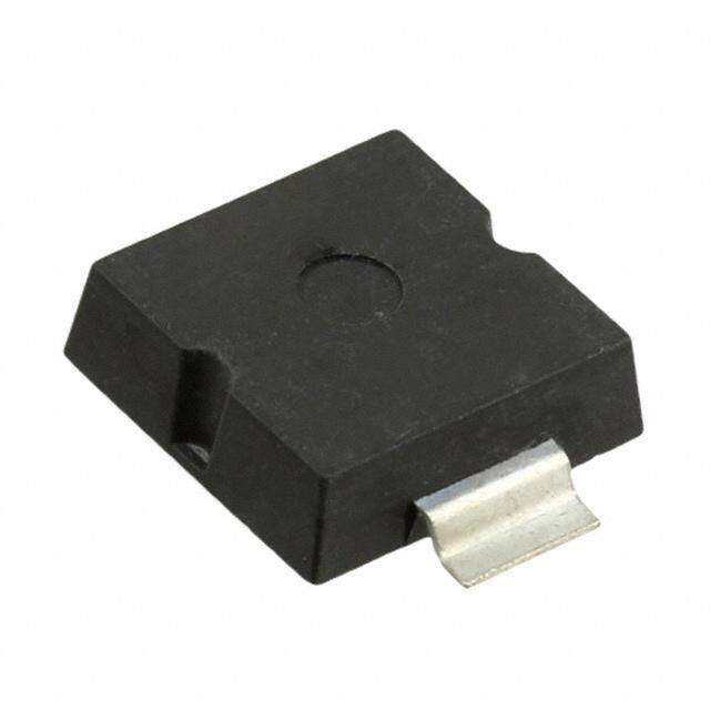
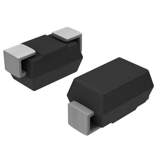
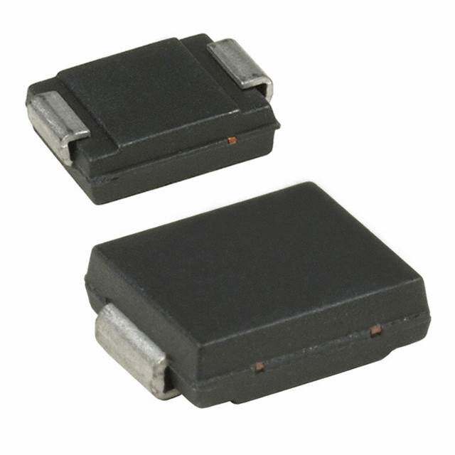
| 描述 | TVS DIODE 5VWM 22VC DFN1006 |
| 产品分类 | |
| 品牌 | Alpha & Omega Semiconductor Inc |
| 数据手册 | |
| 产品图片 |
|
| 产品型号 | AOZ8131DI-05L |
| PCN组件/产地 | |
| rohs | 无铅 / 符合限制有害物质指令(RoHS)规范要求 |
| 产品系列 | - |
| 不同频率时的电容 | 1.25pF @ 1MHz |
| 供应商器件封装 | DFN1006 |
| 其它名称 | 785-1645-2 |
| 功率-峰值脉冲 | - |
| 包装 | 带卷 (TR) |
| 单向通道 | - |
| 双向通道 | 1 |
| 安装类型 | 表面贴装 |
| 封装/外壳 | 2-UFDFN |
| 工作温度 | -40°C ~ 125°C (TJ) |
| 应用 | 通用 |
| 标准包装 | 10,000 |
| 电压-击穿(最小值) | 6V |
| 电压-反向关态(典型值) | 5V(最小值) |
| 电压-箝位(最大值)@Ipp | 22V |
| 电流-峰值脉冲(10/1000µs) | 4A (8/20µs) |
| 电源线路保护 | 无 |
| 类型 | 齐纳 |


- 商务部:美国ITC正式对集成电路等产品启动337调查
- 曝三星4nm工艺存在良率问题 高通将骁龙8 Gen1或转产台积电
- 太阳诱电将投资9.5亿元在常州建新厂生产MLCC 预计2023年完工
- 英特尔发布欧洲新工厂建设计划 深化IDM 2.0 战略
- 台积电先进制程称霸业界 有大客户加持明年业绩稳了
- 达到5530亿美元!SIA预计今年全球半导体销售额将创下新高
- 英特尔拟将自动驾驶子公司Mobileye上市 估值或超500亿美元
- 三星加码芯片和SET,合并消费电子和移动部门,撤换高东真等 CEO
- 三星电子宣布重大人事变动 还合并消费电子和移动部门
- 海关总署:前11个月进口集成电路产品价值2.52万亿元 增长14.8%


PDF Datasheet 数据手册内容提取
AOZ8131 Ultra Low Capacitance One-Line Bi-directional TVS Diode General Description Features The AOZ8131 is an ultra low capacitance one-line ESD protection for high-speed data lines: bi-directional transient voltage suppressor diode – Exceeds: designed to protect high speed data lines and voltage IEC 61000-4-2 (ESD) ±24kV (air), ±24kV (contact) sensitive electronics from high transient conditions and IEC 61000-4-4(EFT) ±40A (5/50nS) ESD. IEC 61000-4-5 (Lightning) ±4A – Human Body Model (HBM) ±30kV This device incorporates one TVS diode in an ultra-small DFN 1006 package. It may be used to meet the ESD Small package saves board space immunity requirements of IEC 61000-4-2, Ultra low capacitance: 1.25pF Level 4 (±15kV air, ±8kV contact discharge). Low clamping voltage The AOZ8131 comes in an RoHS compliant DFN 1006 Low operating voltage: 5.0V package and is rated over a -40°C to +85°C ambient Pb-free device temperature range. Applications The ultra-small 1.0 x 0.6 x 0.5mm DFN package makes it ideal for applications where PCB space is a premium. Portable handheld devices The small size and high ESD protection makes it ideal for Keypads, data lines, buttons protecting voltage sensitive electronics from high tran- Notebook computers sient conditions and ESD. Digital Cameras Portable GPS MP3 players Typical Application Pin Configuration Signal Line 1 2 Bidirection Protection of Single Line Rev. 3.0 June 2014 www.aosmd.com Page 1 of 6
AOZ8131 Ordering Information Part Number Ambient Temperature Range Package Environmental AOZ8131DI-05L -40°C to +85°C DFN 1006 RoHS Compliant Green Product AOS Green Products use reduced levels of Halogens, and are also RoHS compliant. Please visit www.aosmd.com/media/AOSGreenPolicy.pdf for additional information. Absolute Maximum Ratings Exceeding the Absolute Maximum ratings may damage the device. Parameter Rating Peak Pulse Current (I ), t = 8/20µs 4A PP P Storage Temperature (T ) -65°C to +150°C S ESD Rating per IEC61000-4-2, Contact(1) ±24kV ESD Rating per IEC61000-4-2, Air(1) ±24kV ESD Rating per Human Body Model(2) ±30kV Notes: 1. IEC 61000-4-2 discharge with C = 150pF, R = 330Ω. Discharge Discharge 2. Human Body Discharge per MIL-STD-883, Method 3015 C = 100pF, R = 1.5kΩ. Discharge Discharge Maximum Operating Ratings Parameter Rating Junction Temperature (T ) -40°C to +125°C J Electrical Characteristics T = 25°C unless otherwise specified. A Symbol Parameter Symbol Parameter I Maximum Reverse Peak Pulse Current I Test Current PP T V Clamping Voltage @ I (IEC61000-4-5 8/20µs pulse) P Peak Power Dissipation CL PP pk (IEC61000-4-5 8/20µs pulse) V Working Peak Reverse Voltage RWM I Maximum Reverse Leakage Current C Max. Capacitance @ V = 0 and f = 1MHz R J R V Breakdown Voltage BR Electrical Characteristics T = 25°C unless otherwise noted. A V (V) V Max. C (pF) BR CL J Device VRWM (V) Min. IR (µA) Device Marking Max. IT = 1mA Max. IPP = 2A IPP = 4A Ppk (W) Typ. Max. AOZ8131DI-05L B 5.0 6.0 0.1 14.50 18.50 75 1.25 2.0 Rev. 3.0 June 2014 www.aosmd.com Page 2 of 6
AOZ8131 Typical Performance Characteristics Clamping Voltage vs. Peak Pulse Current Clamping Voltage vs. Peak Pulse Current (tperiod = 100ns, tr = 1ns) (IEC6100-4-5 8/20µs pulse current) 24 20 V) 22 19 ping Voltage, V (CL 211086 Peak Voltage (V) 111876 m a 14 15 Cl 12 14 0 2 4 6 8 10 12 2.0 2.5 3.0 3.5 4.0 Peak Pulse Current, IPP (A) Peak Pulse Current (A) Rev. 3.0 June 2014 www.aosmd.com Page 3 of 6
AOZ8131 Package Dimensions, DFN 1.0 x 0.6 5 2x aaa C (E/4xD)Index Are A 3 e a Pin#1 ID aa D 2x b 0.125x45° a C 2x ddd C AB E B ddd C AB L2 TOP VIEW BOTTOM VIEW 6 A Seating Plane 2x ccc C 7 C A1 SIDE VIEW RECOMMENDED LAND PATTERN Dimensions in millimeters Dimensions in inches Symbols Min. Nom. Max. Symbols Min. Nom. Max. 1.00 A 0.47 0.51 0.55 A 0.019 0.020 0.022 A1 0.00 0.02 0.05 A1 0.000 0.001 0.002 0.30 b 0.45 0.50 0.55 b 0.018 0.020 0.022 D 0.60 BSC D 0.024 E 1.00 BSC E 0.039 0.55 e 0.65 BSC e 0.026 L 0.20 0.25 0.30 L 0.008 0.010 0.012 aaa 0.05 aaa 0.002 0.40 0.125 x 45° ccc 0.03 ccc 0.001 ddd 0.10 ddd 0.004 0.30 UNIT: mm Notes: 1. Dimensions and tolerancing conform to ASME Y14.5-2009. 2. All dimensions are in milliteters. 3. “e” represents the terminal grid pitch. 4. N isthe total number of terminals. 5. A visual index feature must be located within the hatched area. Typical index feature (chamfer) must be located on the edge of the Pin#1 feature. 6. This dimension includes stand-off height “A1” and packaged body thickness, but does not include attached feature e.g. external heatsink or chip capacitors, an internal heatslug is not considered as attached feature. 7. Dimension “A1” is primarily terminal plating, and does not include small metal protrusions. Rev. 3.0 June 2014 www.aosmd.com Page 4 of 6
AOZ8131 Tape and Reel Dimensions, DFN 1.0 x 0.6 Carrier Tape P1 P2 T D1 E1 E2 E B0 K0 A0 D0 P0 UNIT: mm Option Package A0 B0 K0 D0 D1 E E1 E2 P0 P1 P2 T DFN 1.0x0.6/ 0.69 1.19 0.66 0.40 1.50 8.00 1.75 3.50 2.00 4.00 2.00 0.23 A DFN 1.0x0.6A ±0.05 ±0.05 ±0.05 ±0.05 ±0.10 +0.3/-0.1 ±0.10 ±0.05 ±0.05 ±0.10 ±0.05 ±0.02 (8 mm) DFN 1.0x0.6/ 0.65 1.05 0.61 0.40 1.50 8.00 1.75 3.50 2.00 4.00 2.00 0.20 B DFN 1.0x0.6A ±0.04 ±0.04 ±0.04 ±0.05 ±0.10 +0.3/-0.1 ±0.10 ±0.05 ±0.10 ±0.10 ±0.05 ±0.05 (8 mm) Reel W1 S G N M K V R H W UNIT: mm Tape Size Reel Size M N W W1 H K S G R V 8mm ø178 ø178 ø55 8.4 Max. ø13.0 Max. 2.0 N/A N/A N/A ±0.5 ±1 +1.5/-0 14.4 ±0.5 10.1 ±0.5 Leader/Trailer & Orientation TVS Unit Per Reel: 10000pcs Trailer Tape Components Tape Leader Tape 300mm Min. Orientation in Pocket 500mm Min. Rev. 3.0 June 2014 www.aosmd.com Page 5 of 6
AOZ8131 Part Marking B E Product Number Code Date Code LEGAL DISCLAIMER Alpha and Omega Semiconductor makes no representations or warranties with respect to the accuracy or completeness of the information provided herein and takes no liabilities for the consequences of use of such information or any product described herein.Alpha and Omega Semiconductor reserves the right to make changes to such information at any time without further notice. This document does not constitute the grant of any intellectual property rights or representation of non-infringement of any third party’s intellectual property rights. LIFE SUPPORT POLICY ALPHA AND OMEGA SEMICONDUCTOR PRODUCTS ARE NOT AUTHORIZED FOR USE AS CRITICAL COMPONENTS IN LIFE SUPPORT DEVICES OR SYSTEMS. As used herein: 1. Life support devices or systems are devices or 2. A critical component in any component of a life systems which, (a) are intended for surgical implant into support, device, or system whose failure to perform can the body or (b) support or sustain life, and (c) whose be reasonably expected to cause the failure of the life failure to perform when properly used in accordance support device or system, or to affect its safety or with instructions for use provided in the labeling, can be effectiveness. reasonably expected to result in a significant injury of the user. Rev. 3.0 June 2014 www.aosmd.com Page 6 of 6