 Datasheet下载
- 型号: ADV7280KCPZ
- 制造商: Analog
- 库位|库存: xxxx|xxxx
- 要求:
| 数量阶梯 | 香港交货 | 国内含税 |
| +xxxx | $xxxx | ¥xxxx |
查看当月历史价格
查看今年历史价格
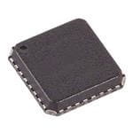
ADV7280KCPZ产品简介:
ICGOO电子元器件商城为您提供ADV7280KCPZ由Analog设计生产,在icgoo商城现货销售,并且可以通过原厂、代理商等渠道进行代购。 ADV7280KCPZ价格参考¥37.96-¥54.17。AnalogADV7280KCPZ封装/规格:接口 - 编解码器, Video Interface 10 b I²C, Serial 32-LFCSP-WQ (5x5)。您可以下载ADV7280KCPZ参考资料、Datasheet数据手册功能说明书,资料中有ADV7280KCPZ 详细功能的应用电路图电压和使用方法及教程。
ADV7280KCPZ 是由 Analog Devices Inc.(ADI)生产的一款接口编解码器芯片,属于视频处理领域的产品。其主要应用场景包括以下几方面:

1. 视频监控系统:ADV7280KCPZ 可用于安防摄像头或 DVR(数字视频录像机)中,支持复合视频信号(CVBS)和 S-Video 的解码,将模拟视频信号转换为数字格式以便存储、传输或进一步处理。

2. 医疗成像设备:在超声波设备、内窥镜等需要处理模拟视频输入的医疗仪器中,该芯片能够实现高质量的视频数字化,确保图像清晰度和实时性。

3. 工业自动化:适用于机器视觉系统或其他需要分析视频流的工业应用。它可将来自摄像机的模拟信号转换为便于计算机处理的数字数据。

4. 消费电子产品:如 DVD 播放器、游戏主机或家庭影音中心等设备中,ADV7280KCPZ 能够处理多种标准定义的视频输入,并提供稳定的输出性能。

5. 汽车电子:倒车摄像头、行车记录仪等车载显示系统可以利用此芯片进行视频信号的采集与处理,满足对可靠性和环境适应性的严格要求。

总结来说,ADV7280KCPZ 主要用于需要将模拟视频信号转换为数字信号的各种场合,涵盖从专业级到消费级的应用范围,具有良好的兼容性和灵活性。
| 参数 | 数值 |
| ADC/DAC数 | 1 / 0 |
| 产品目录 | 集成电路 (IC)半导体 |
| 描述 | IC VIDEO DECODER SDTV 32-LFCSP视频 IC 10-bit SD Video Decoder |
| 产品分类 | |
| 品牌 | Analog Devices Inc |
| 产品手册 | |
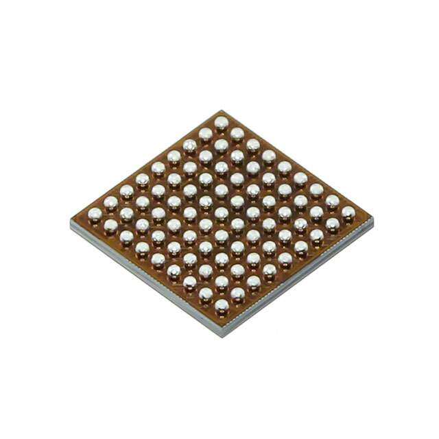
| 产品图片 | |
| rohs | 符合RoHS无铅 / 符合限制有害物质指令(RoHS)规范要求 |
| 产品系列 | 多媒体 IC,视频 IC,Analog Devices ADV7280KCPZ- |
| 数据手册 | |
| 产品型号 | ADV7280KCPZ |
| PCN组件/产地 | |
| 三角积分 | - |
| 产品种类 | 视频 IC |
| 供应商器件封装 | 32-LFCSP-WQ(5x5) |
| 信噪比,ADC/DAC(db)(典型值) | - |
| 分辨率 | 10 bit |
| 分辨率(位) | 10 b |
| 动态范围,ADC/DAC(db)(典型值) | - |
| 包装 | 托盘 |
| 商标 | Analog Devices |
| 安装类型 | 表面贴装 |
| 安装风格 | SMD/SMT |
| 封装 | Tray |
| 封装/外壳 | 32-WFQFN 裸露焊盘,CSP |
| 封装/箱体 | LFCSP-20 |
| 工作温度 | -10°C ~ 70°C |
| 工厂包装数量 | 490 |
| 数据接口 | I²C, 串行 |
| 最大功率耗散 | 1 mW |
| 最大工作温度 | + 70 C |
| 最小工作温度 | - 10 C |
| 标准包装 | 1 |
| 电压-电源,数字 | 1.71 V ~ 1.89 V |
| 电压-电源,模拟 | 1.71 V ~ 1.89 V |
| 电源电流 | 5 mA |
| 端接类型 | SMD/SMT |
| 类型 | 视频 |
| 通道数量 | 4 Channel |
| 配用 | /product-detail/zh/EVAL-ADV7280EBZ/EVAL-ADV7280EBZ-ND/4866762 |


- 商务部:美国ITC正式对集成电路等产品启动337调查
- 曝三星4nm工艺存在良率问题 高通将骁龙8 Gen1或转产台积电
- 太阳诱电将投资9.5亿元在常州建新厂生产MLCC 预计2023年完工
- 英特尔发布欧洲新工厂建设计划 深化IDM 2.0 战略
- 台积电先进制程称霸业界 有大客户加持明年业绩稳了
- 达到5530亿美元!SIA预计今年全球半导体销售额将创下新高
- 英特尔拟将自动驾驶子公司Mobileye上市 估值或超500亿美元
- 三星加码芯片和SET,合并消费电子和移动部门,撤换高东真等 CEO
- 三星电子宣布重大人事变动 还合并消费电子和移动部门
- 海关总署:前11个月进口集成电路产品价值2.52万亿元 增长14.8%


PDF Datasheet 数据手册内容提取
10-Bit, 4× Oversampled SDTV Video Decoder with Deinterlacer Data Sheet ADV7280 FEATURES APPLICATIONS Worldwide NTSC/PAL/SECAM color demodulation support Smartphone/multimedia handsets One 10-bit analog-to-digital converter (ADC), 4× oversampling Automotive infotainment per channel for CVBS, Y/C, and YPrPb modes DVRs for video security Analog video input channels with on-chip antialiasing filter Media players ADV7280: up to 4 input channels GENERAL DESCRIPTION ADV7280-M: up to 8 input channels Video input support for CVBS (composite), Y/C (S-Video), The ADV7280/ADV7280-M are versatile one-chip, multiformat and YPrPb (component) video decoders. The ADV7280/ADV7280-M automatically detect NTSC/PAL/SECAM autodetection standard analog baseband video signals compatible with worldwide Up to 1.47 V common-mode input range solution NTSC, PAL, and SECAM standards in the form of composite, Excellent common-mode noise rejection capabilities S-Video, and component video. 5-line adaptive 2D comb filter and CTI video enhancement The ADV7280 converts the analog video signals into a YCrCb Adaptive Digital Line Length Tracking (ADLLT), signal 4:2:2 video data stream that is compatible with the 8-bit ITU-R processing, and enhanced FIFO management provide BT.656 interface standard. The ADV7280-M converts the analog mini-time base correction (TBC) functionality video signals into an 8-bit YCrCb 4:2:2 video data stream that is Integrated automatic gain control (AGC) with adaptive output over a mobile industry processor interface (MIPI®) CSI-2 peak white mode interface. Fast switching capability The analog video inputs of the ADV7280/ADV7280-M accept Integrated interlaced-to-progressive (I2P) video output single-ended signals. The ADV7280 provides four analog inputs; converter the ADV7280-M provides eight analog inputs. The ADV7280 Adaptive contrast enhancement (ACE) and ADV7280-M support I2P conversion. Down dither (8-bit to 6-bit) Rovi (Macrovision) copy protection detection The ADV7280/ADV7280-M are programmed via a 2-wire, MIPI CSI-2 output interface (ADV7280-M) serial bidirectional port (I2C compatible) and are fabricated in a 8-bit ITU-R BT.656 YCrCb 4:2:2 output and HS, VS, or field 1.8 V CMOS process. The LFCSP package option makes these synchronization (ADV7280) decoders ideal for space-constrained portable applications. Full featured vertical blanking interval (VBI) data slicer Power-down mode available 2-wire, I2C-compatible serial interface Qualified for automotive applications −40°C to +105°C temperature grade 32-lead, 5 mm × 5 mm, RoHS-compliant LFCSP Rev. A Document Feedback Information furnished by Analog Devices is believed to be accurate and reliable. However, no responsibility is assumed by Analog Devices for its use, nor for any infringements of patents or other One Technology Way, P.O. Box 9106, Norwood, MA 02062-9106, U.S.A. rights of third parties that may result from its use. Specifications subject to change without notice. No license is granted by implication or otherwise under any patent or patent rights of Analog Devices. Tel: 781.329.4700 ©2013–2014 Analog Devices, Inc. All rights reserved. Trademarks and registered trademarks are the property of their respective owners. Technical Support www.analog.com
ADV7280 Data Sheet TABLE OF CONTENTS Features .............................................................................................. 1 Power-Down Sequence .............................................................. 15 Applications ....................................................................................... 1 Universal Power Supply (ADV7280 Only) ............................. 15 General Description ......................................................................... 1 Input Network ................................................................................. 16 Revision History ............................................................................... 2 Input Configuration ....................................................................... 17 Functional Block Diagrams ............................................................. 3 Adaptive Contrast Enhancement (ACE) ..................................... 18 Specifications ..................................................................................... 4 I2P Function .................................................................................... 19 Electrical Specifications ............................................................... 4 MIPI CSI-2 Output (ADV7280-M Only) ................................... 20 Video Specifications ..................................................................... 5 ITU-R BT.656 Tx Configuration (ADV7280 Only) .................. 21 Analog Specifications ................................................................... 6 I2C Port Description ....................................................................... 22 MIPI Video Output Specifications (ADV7280-M Only) ........ 6 Register Maps .............................................................................. 23 Pixel Port Timing Specifications (ADV7280 Only) ................. 8 PCB Layout Recommendations .................................................... 25 Clock and I2C Timing Specifications ......................................... 9 Analog Interface Inputs ............................................................. 25 Absolute Maximum Ratings .......................................................... 10 Power Supply Decoupling ......................................................... 25 Thermal Resistance .................................................................... 10 VREFN and VREFP Pins .......................................................... 25 Reflow Solder .............................................................................. 10 Digital Outputs (INTRQ, GPO0 to GPO2) ............................ 25 ESD Caution ................................................................................ 10 Exposed Metal Pad ..................................................................... 25 Pin Configurations and Function Descriptions ......................... 11 Digital Inputs .............................................................................. 25 Theory of Operation ...................................................................... 13 MIPI Outputs for the ADV7280-M (D0P, D0N, Analog Front End (AFE) ........................................................... 13 CLKP, CLKN) ............................................................................. 25 Standard Definition Processor (SDP) ...................................... 14 Typical Circuit Connections ......................................................... 26 Power Supply Sequencing .............................................................. 15 Outline Dimensions ....................................................................... 28 Optimal Power-Up Sequence .................................................... 15 Ordering Guide .......................................................................... 28 Simplified Power-Up Sequence ................................................ 15 Automotive Products ................................................................. 28 REVISION HISTORY 2/14—Rev. 0 to Rev. A 8/13—Revision 0: Initial Version Change to Single-Ended CVBS Input Parameter, Analog Supply Current, Table 1 ................................................................................ 4 Rev. A | Page 2 of 28
Data Sheet ADV7280 FUNCTIONAL BLOCK DIAGRAMS ADV7280 CLOCK PROCESSING BLOCK XTALP PLL ADLLT PROCESSING LLC XTALN 10-BIT ADC DIGITAL VS/FIELD/SFL AAIINN12 CK FILAATAAER PR2OBDCL CEOOSCMSKIBNG FIFOK ACE H8-SBIT ANAILNOPGU TVSIDEO AAIINN34 MUX BLO FFFIIILLLAATTTAAEEERRR +–SHA ADC VBDCIE OSIM2LLPOOICRDER OUTPUT BLOC DDIOTHWENR PPI7X TEOL DP0ATA REFERENCE I2C/CONTROL INTRQ SCLKSDATAALSB RESET PWRDWN 11634-001 Figure 1. ADV7280 Functional Block Diagram ADV7280-M CLOCK PROCESSING BLOCK CLKP XTALP MIPI CLKN PLL ADLLT PROCESSING Tx D0P XTALN D0N 10-BIT ADC DIGITAL AAIINN12 K FILATAER PR2OBDCL CEOOSCMSKIBNG FIFO ACE ANAILNOPGU TVSIDEO AAAAAAIIIIIINNNNNN785634 MUX BLOC FFFIIILLLAAATTTAAAEEERRR +–SHA ADC VBDCIE OSIM2LLPOOICRDER OUTPUT BLOCK DDIOTHWENR GGGPPPOOO012 REFERENCE I2C/CONTROL INTRQ SCLKSDATAALSB RESET PWRDWN 11634-002 Figure 2. ADV7280-M Functional Block Diagram Rev. A | Page 3 of 28
ADV7280 Data Sheet SPECIFICATIONS ELECTRICAL SPECIFICATIONS A , D , P , and M = 1.71 V to 1.89 V, D = 2.97 V to 3.63 V, specified at operating temperature range, unless otherwise noted. VDD VDD VDD VDD VDDIO M applies to the ADV7280-M only. VDD Table 1. Parameter Symbol Test Conditions/Comments Min Typ Max Unit STATIC PERFORMANCE ADC Resolution N 10 Bits Integral Nonlinearity INL CVBS mode 2 LSB Differential Nonlinearity DNL CVBS mode ±0.6 LSB DIGITAL INPUTS Input High Voltage V D = 3.3 V 2 V IH VDDIO D = 1.8 V, ADV7280 only 1.2 V VDDIO Input Low Voltage V D = 3.3 V 0.8 V IL VDDIO D = 1.8 V, ADV7280 only 0.4 V VDDIO Input Leakage Current I RESET pin −10 +10 µA IN SDATA, SCLK pins −10 +15 µA PWRDWN, ALSB pins −10 +50 µA Input Capacitance C 10 pF IN CRYSTAL INPUT Input High Voltage V XTALN pin 1.2 V IH Input Low Voltage V XTALN pin 0.4 V IL DIGITAL OUTPUTS Output High Voltage V D = 3.3 V, I = 0.4 mA 2.4 V OH VDDIO SOURCE D = 1.8 V, I = 0.4 mA, 1.4 V VDDIO SOURCE ADV7280 only Output Low Voltage V D = 3.3 V, I = 3.2 mA 0.4 V OL VDDIO SINK D = 1.8 V, I = 1.6 mA, 0.2 V VDDIO SINK ADV7280 only High Impedance Leakage Current I 10 µA LEAK Output Capacitance C 20 pF OUT POWER REQUIREMENTS1, 2, 3 Digital I/O Power Supply D ADV7280-M 2.97 3.3 3.63 V VDDIO ADV7280 1.62 3.3 3.63 V PLL Power Supply P 1.71 1.8 1.89 V VDD Analog Power Supply A 1.71 1.8 1.89 V VDD Digital Power Supply D 1.71 1.8 1.89 V VDD MIPI Tx Power Supply M ADV7280-M only 1.71 1.8 1.89 V VDD Digital I/O Supply Current I ADV7280-M 1.5 mA DVDDIO ADV7280 5 mA PLL Supply Current I 12 mA PVDD MIPI Tx Supply Current I ADV7280-M only 14 mA MVDD Analog Supply Current I AVDD Single-Ended CVBS Input 47 mA Y/C Input 60 mA YPrPb Input 75 mA Digital Supply Current I DVDD Single-Ended CVBS Input 70 mA Y/C Input 70 mA YPrPb Input 70 mA Rev. A | Page 4 of 28
Data Sheet ADV7280 Parameter Symbol Test Conditions/Comments Min Typ Max Unit POWER-DOWN CURRENTS1 Digital I/O Supply Power-Down Current I D = 3.3 V, ADV7280-M 73 µA DVDDIO_PD VDDIO D = 3.3 V, ADV7280 84 µA VDDIO PLL Supply Power-Down Current I 46 µA PVDD_PD Analog Supply Power-Down Current I 0.2 µA AVDD_PD Digital Supply Power-Down Current I 420 µA DVDD_PD MIPI Tx Supply Power-Down Current I ADV7280-M only 4.5 µA MVDD_PD Total Power Dissipation 1 mW in Power-Down Mode 1 Guaranteed by characterization. 2 Typical current consumption values are measured with nominal voltage supply levels and an SMPTE bar test pattern. 3 All specifications apply when the I2P core is activated, unless otherwise stated. VIDEO SPECIFICATIONS A , D , P , and M = 1.71 V to 1.89 V, D = 2.97 V to 3.63 V, specified at operating temperature range, unless otherwise noted. VDD VDD VDD VDD VDDIO Specifications guaranteed by characterization. M applies to the ADV7280-M only. VDD Table 2. Parameter Symbol Test Conditions/Comments Min Typ Max Unit NONLINEAR SPECIFICATIONS1 Differential Phase DP CVBS input, modulated 5-step 0.9 Degrees Differential Gain DG CVBS input, modulated 5-step 0.5 % Luma Nonlinearity LNL CVBS input, 5-step 2.0 % NOISE SPECIFICATIONS Signal-to-Noise Ratio, Unweighted SNR Luma ramp 57.1 dB Luma flat field 58 dB Analog Front-End Crosstalk 60 dB Common-Mode Rejection Ratio2 CMRR 73 dB LOCK TIME SPECIFICATIONS Horizontal Lock Range −5 +5 % Vertical Lock Range 40 70 Hz f Subcarrier Lock Range ±1.3 kHz SC Color Lock-In Time 60 Lines Synchronization Depth Range 20 200 % Color Burst Range 5 200 % Vertical Lock Time 2 Fields Autodetection Switch Speed3 100 Lines Fast Switch Speed4 100 ms LUMA SPECIFICATIONS CVBS, 1 V input Luma Brightness Accuracy 1 % Luma Contrast Accuracy 1 % 1 These specifications apply for all CVBS input types (NTSC, PAL, and SECAM). 2 The CMRR of this circuit design is critically dependent on the external resistor matching on the circuit inputs (see the Input Network section). The CMRR measurement was performed with 0.1% tolerant resistors, a common-mode voltage of 1 V, and a common-mode frequency of 10 kHz. 3 Autodetection switch speed is the time required for the ADV7280/ADV7280-M to detect which video format is present at its input, for example, PAL I or NTSC M. 4 Fast switch speed is the time required for the ADV7280/ADV7280-M to switch from one analog input to another, for example, switching from AIN1 to AIN2. Rev. A | Page 5 of 28
ADV7280 Data Sheet ANALOG SPECIFICATIONS A , D , P , and M = 1.71 V to 1.89 V, D = 2.97 V to 3.63 V, specified at operating temperature range, unless otherwise noted. VDD VDD VDD VDD VDDIO Specifications guaranteed by characterization. M applies to the ADV7280-M only. VDD Table 3. Parameter Test Conditions/Comments Min Typ Max Unit CLAMP CIRCUITRY External Clamp Capacitor 0.1 µF Input Impedance Clamps switched off 10 MΩ Large Clamp Source Current 0.4 mA Large Clamp Sink Current 0.4 mA Fine Clamp Source Current 10 µA Fine Clamp Sink Current 10 µA MIPI VIDEO OUTPUT SPECIFICATIONS (ADV7280-M ONLY) A , D , P , and M = 1.71 V to 1.89 V, D = 2.97 V to 3.63 V, specified at operating temperature range, unless otherwise noted. VDD VDD VDD VDD VDDIO The CSI-2 clock lane of the ADV7280-M remains in high speed (HS) mode even when the data lane enters low power (LP) mode. For this reason, some measurements on the clock lane that pertain to low power mode are not applicable. Unless otherwise stated, all high speed measurements were performed with the ADV7280-M operating in progressive mode and with a nominal 432 Mbps output data rate. Specifications guaranteed by characterization. Table 4. Parameter Symbol Test Conditions/Comments Min Typ Max Unit UNIT INTERVAL UI Interlaced Output 4.63 ns Progressive Output 2.31 ns DATA LANE LP TX DC SPECIFICATIONS1 Thevenin Output High Level V 1.1 1.2 1.3 V OH Thevenin Output Low Level V −50 0 +50 mV OL DATA LANE LP TX AC SPECIFICATIONS1 Rise Time, 15% to 85% 25 ns Fall Time, 85% to 15% 25 ns Rise Time, 30% to 85% 35 ns Data Lane LP Slew Rate vs. C LOAD Maximum Slew Rate over Entire Rising edge 150 mV/ns Vertical Edge Region Falling edge 150 mV/ns Minimum Slew Rate 400 mV ≤ V ≤ 930 mV Falling edge 30 mV/ns OUT 400 mV ≤ V ≤ 700 mV Rising edge 30 mV/ns OUT 700 mV ≤ V ≤ 930 mV Rising edge >0 mV/ns OUT Pulse Width of LP Exclusive-OR Clock First clock pulse after stop state 40 ns or last pulse before stop state All other clock pulses 20 ns Period of LP Exclusive-OR Clock 90 ns CLOCK LANE LP TX DC SPECIFICATIONS1 Thevenin Output High Level V 1.1 1.2 1.3 V OH Thevenin Output Low Level V −50 0 +50 mV OL CLOCK LANE LP TX AC SPECIFICATIONS1 Rise Time, 15% to 85% 25 ns Fall Time, 85% to 15% 25 ns Rev. A | Page 6 of 28
Data Sheet ADV7280 Parameter Symbol Test Conditions/Comments Min Typ Max Unit Clock Lane LP Slew Rate Maximum Slew Rate over Entire Rising edge 150 mV/ns Vertical Edge Region Falling edge 150 mV/ns Minimum Slew Rate 400 mV ≤ V ≤ 930 mV Falling edge 30 mV/ns OUT 400 mV ≤ V ≤ 700 mV Rising edge 30 mV/ns OUT 700 mV ≤ V ≤ 930 mV Rising edge >0 mV/ns OUT DATA LANE HS TX SIGNALING See Figure 3 REQUIREMENTS Low Power to High Speed Transition t Time that the D0P pin is at V 50 ns 9 OL Stage and the D0N pin is at V OH t Time that the D0P and D0N pins 40 + (4 × UI) 85 + (6 × UI) ns 10 are at V OL t t plus the HS-zero period 145 + (10 × UI) ns 11 10 High Speed Differential Voltage Swing |V| 140 200 270 mV p-p 1 Differential Voltage Mismatch 10 mV Single-Ended Output High Voltages 360 mV Static Common-Mode Voltage Level 150 200 250 mV Static Common-Mode Voltage 5 mV Mismatch Dynamic Common Level Variations 50 MHz to 450 MHz 25 mV Above 450 MHz 15 mV Rise Time, 20% to 80% 0.15 0.3 × UI ns Fall Time, 80% to 20% 0.15 0.3 × UI ns High Speed to Low Power Transition t Time that the ADV7280-M drives 60 + (4 × UI) ns 12 Stage the flipped last data bit after sending the last payload data bit of an HS transmission burst t Post-end-of-transmission rise 35 ns 13 time (30% to 85%) t Time from start of t to start of 105 + (12 × UI) ns 14 12 low power state following an HS transmission burst t Time that a low power state is 100 ns 15 transmitted after an HS trans- mission burst CLOCK LANE HS TX SIGNALING See Figure 3 REQUIREMENTS Low Power to High Speed Transition t Time that the CLKP pin is at V 50 ns 9 OL Stage2 and the CLKN pin is at V OH Time that the CLKP and CLKN 38 95 ns pins are at V OL Clock HS-zero period 300 500 ns High Speed Differential Voltage Swing |V| 140 200 270 mV p-p 2 Differential Voltage Mismatch 10 mV Single-Ended Output High Voltages 360 mV Static Common-Mode Voltage Level 150 200 250 mV Static Common-Mode Voltage 5 mV Mismatch Dynamic Common Level Variations 50 MHz to 450 MHz 25 mV Above 450 MHz 15 mV Rise Time, 20% to 80% 0.15 0.3 × UI ns Fall Time, 80% to 20% 0.15 0.3 × UI ns Rev. A | Page 7 of 28
ADV7280 Data Sheet Parameter Symbol Test Conditions/Comments Min Typ Max Unit HS TX CLOCK TO DATA LANE TIMING REQUIREMENTS Data to Clock Skew 0.35 × UI 0.65 × UI ns 1 These measurements were performed with CLOAD = 50 pF. 2 The clock lane remains in high speed mode throughout normal operation. These results apply only to the ADV7280-M during startup. CLKP/CLKN |V2| D0P/D0N t9 t10 t11 VOH |V1| VOL TRANSMIT FIRST t13 DATA BIT t14 t12 t15 LOW POWER HS-ZERO START OF HIGH SPEED DATA TO TRANSMISSION TRANSMISSION HIGH SPEED SEQUENCE HS-TRAIL HIGH SPEED TRANSITION LTORWANT PSOOITWIOENR 11634-005 Figure 3. ADV7280-M Output Timing Diagram (Conforms with MIPI CSI-2 Specification) PIXEL PORT TIMING SPECIFICATIONS (ADV7280 ONLY) A , D , and P = 1.71 V to 1.89 V, D = 1.62 V to 3.63 V, specified at operating temperature range, unless otherwise noted. VDD VDD VDD VDDIO Specifications guaranteed by characterization. Table 5. Parameter Symbol Test Conditions/Comments Min Typ Max Unit CLOCK OUTPUTS LLC Mark Space Ratio t:t 45:55 55:45 % duty cycle 9 10 DATA AND CONTROL OUTPUTS Data Output Transitional Time t Negative clock edge to start of valid data 3.8 ns 11 (t = t − t ) SETUP 10 11 t End of valid data to negative clock edge 6.9 ns 12 (t = t − t ) HOLD 9 12 t9 t10 OUTPUT LLC t11 t12 OUTPUTS VPS0 /TFOIE LPD7,/ SHFSL, 11634-004 Figure 4. ADV7280 Pixel Port and Control Output Timing Diagram Rev. A | Page 8 of 28
Data Sheet ADV7280 CLOCK AND I2C TIMING SPECIFICATIONS A , D , P , and M = 1.71 V to 1.89 V, D = 2.97 V to 3.63 V, specified at operating temperature range, unless otherwise noted. VDD VDD VDD VDD VDDIO Specifications guaranteed by characterization. M applies to the ADV7280-M only. VDD Table 6. Parameter Symbol Min Typ Max Unit SYSTEM CLOCK AND CRYSTAL Nominal Frequency 28.63636 MHz Frequency Stability ±50 ppm I2C PORT SCLK Frequency 400 kHz SCLK Minimum Pulse Width High t 0.6 µs 1 SCLK Minimum Pulse Width Low t 1.3 µs 2 Hold Time (Start Condition) t 0.6 µs 3 Setup Time (Start Condition) t 0.6 µs 4 SDATA Setup Time t 100 ns 5 SCLK and SDATA Rise Times t 300 ns 6 SCLK and SDATA Fall Times t 300 ns 7 Setup Time (Stop Condition) t 0.6 µs 8 RESET INPUT RESET Pulse Width 5 ms t3 t5 t3 SDATA t6 t1 SCLK t2 t7 t4 t8 11634-003 Figure 5. I2C Timing Diagram Rev. A | Page 9 of 28
ADV7280 Data Sheet ABSOLUTE MAXIMUM RATINGS THERMAL RESISTANCE Table 7. Parameter Rating The thermal resistance values in Table 8 are specified for the AVDD to DGND 2.2 V device soldered onto a 4-layer printed circuit board (PCB) with DVDD to DGND 2.2 V a common ground plane and with the exposed pad of the device PVDD to DGND 2.2 V connected to DGND. The values in Table 8 are maximum values. M to DGND1 2.2 V VDD D to DGND 4 V Table 8. Thermal Resistance for the 32-Lead LFCSP VDDIO P to D −0.9 V to +0.9 V Thermal Characteristic Symbol Value Unit VDD VDD MVDD to DVDD1 −0.9 V to +0.9 V Junction-to-Ambient Thermal θJA 32.5 °C/W Resistance (Still Air) A to D −0.9 V to +0.9 V VDD VDD Junction-to-Case Thermal θ 2.3 °C/W Digital Inputs Voltage DGND − 0.3 V to D + 0.3 V JC VDDIO Resistance Digital Outputs Voltage DGND − 0.3 V to D + 0.3 V VDDIO Analog Inputs to Ground Ground − 0.3 V to A + 0.3 V REFLOW SOLDER VDD Maximum Junction Temperature 140°C The ADV7280/ADV7280-M are Pb-free, environmentally (T max) J friendly products. They are manufactured using the most up-to- Storage Temperature Range −65°C to +150°C date materials and processes. The coating on the leads of each Infrared Reflow Soldering 260°C (20 sec) device is 100% pure Sn electroplate. The devices are suitable for Pb-free applications and can withstand surface-mount soldering 1 MVDD applies to the ADV7280-M only. at up to 255°C (±5°C). Stresses above those listed under Absolute Maximum Ratings In addition, the ADV7280/ADV7280-M are backward- may cause permanent damage to the device. This is a stress compatible with conventional SnPb soldering processes. This rating only; functional operation of the device at these or any means that the electroplated Sn coating can be soldered with other conditions above those indicated in the operational Sn/Pb solder pastes at conventional reflow temperatures of section of this specification is not implied. Exposure to absolute 220°C to 235°C. maximum rating conditions for extended periods may affect device reliability. ESD CAUTION These devices are high performance integrated circuits with an ESD rating of <2 kV, and they are ESD sensitive. Proper precautions must be taken for handling and assembly. Rev. A | Page 10 of 28
Data Sheet ADV7280 PIN CONFIGURATIONS AND FUNCTION DESCRIPTIONS L F S N D/ LCWRDWSS/FIELCLKDATALSBESET LPHVSSAR 21098765 33322222 DGND 1 24 INTRQ DVDDIO 2 23 AIN4 DVDD 3 ADV7280 22 AIN3 DGND 4 TOP VIEW 21 AVDD P7 5 (Not to Scale) 20 VREFN P6 6 19 VREFP P5 7 18 AIN2 P4 8 17 AIN1 90123456 1111111 3210 DPN D N1.OTTHEES EXPOSED PPADP MPUSPT DBVDEXTAL COXTALNPNVDECTED TO DGND. 11634-006 Figure 6. Pin Configuration, ADV7280 Table 9. Pin Function Descriptions, ADV7280 Pin No. Mnemonic Type Description 1, 4 DGND Ground Ground for Digital Supply. 2 D Power Digital I/O Power Supply (1.8 V or 3.3 V). VDDIO 3, 13 D Power Digital Power Supply (1.8 V). VDD 5 to 12 P7 to P0 Output Video Pixel Output Ports. 14 XTALP Output Connect this pin to the external 28.63636 MHz crystal, or leave it unconnected if an external 1.8 V, 28.63636 MHz clock oscillator source is used to clock the ADV7280. The crystal used with the ADV7280 must be a fundamental crystal. 15 XTALN Input Input Pin for the External 28.63636 MHz Crystal. The crystal used with the ADV7280 must be a fundamental crystal. If an external 1.8 V, 28.63636 MHz clock oscillator source is used to clock the ADV7280, the output of the oscillator is fed into the XTALN pin. 16 P Power PLL Power Supply (1.8 V). VDD 17, 18, A 1 to A 4 Input Analog Video Input Channels. IN IN 22, 23 19 VREFP Output Internal Voltage Reference Output. 20 VREFN Output Internal Voltage Reference Output. 21 A Power Analog Power Supply (1.8 V). VDD 24 INTRQ Output Interrupt Request Output. An interrupt occurs when certain signals are detected on the input video. 25 RESET Input System Reset Input (Active Low). A minimum low reset pulse width of 5 ms is required to reset the ADV7280 circuitry. 26 ALSB Input This pin selects the I2C write address for the ADV7280. When ALSB is set to Logic 0, the write address is 0x40; when ALSB is set to Logic 1, the write address is 0x42. 27 SDATA Input/output I2C Port Serial Data Input/Output. 28 SCLK Input I2C Port Serial Clock Input. The maximum clock rate is 400 kHz. 29 VS/FIELD/SFL Output Vertical Synchronization Output Signal/Field Synchronization Output Signal/Subcarrier Frequency Lock. When configured for the SFL function, this pin provides a serial output stream that can be used to lock the subcarrier frequency when the ADV7280 decoder is connected to any Analog Devices, Inc., digital video encoder. 30 HS Output Horizontal Synchronization Output Signal. 31 PWRDWN Input Power-Down Pin. A logic low on this pin places the ADV7280 in power-down mode. 32 LLC Output Line-Locked Output Clock for Output Pixel Data. The clock output is nominally 27 MHz, but it increases or decreases according to the video line length. EPAD (EP) Exposed Pad. The exposed pad must be connected to DGND. Rev. A | Page 11 of 28
ADV7280 Data Sheet N W PWRDSCLKSDATAALSBRESET8AINA7INA6IN 21098765 33322222 DGND 1 24 AIN5 DVDDIO 2 23 AIN4 DVDD 3 ADV7280-M 22 AIN3 DGND 4 TOP VIEW 21 AVDD INTRQ 5 (Not to Scale) 20 VREFN GPO2 6 19 VREFP GPO1 7 18 AIN2 GPO0 8 17 AIN1 90123456 1111111 PNPN DPN D N1.OTTHEES EXPOSED PD0ADD0 MCLKUSCLKT MBVDEXTAL COXTALNPNVDECTED TO DGND. 11634-007 Figure 7. Pin Configuration, ADV7280-M Table 10. Pin Function Descriptions, ADV7280-M Pin No. Mnemonic Type Description 1, 4 DGND Ground Ground for Digital Supply. 2 D Power Digital I/O Power Supply (3.3 V). VDDIO 3 D Power Digital Power Supply (1.8 V). VDD 5 INTRQ Output Interrupt Request Output. An interrupt occurs when certain signals are detected on the input video. 6 to 8 GPO2 to Output General-Purpose Outputs. These pins can be configured via I2C to allow control of external GPO0 devices. 9 D0P Output Positive MIPI Differential Data Output. 10 D0N Output Negative MIPI Differential Data Output. 11 CLKP Output Positive MIPI Differential Clock Output. 12 CLKN Output Negative MIPI Differential Clock Output. 13 M Power MIPI Digital Power Supply (1.8 V). VDD 14 XTALP Output Connect this pin to the external 28.63636 MHz crystal, or leave it unconnected if an external 1.8 V, 28.63636 MHz clock oscillator source is used to clock the ADV7280-M. The crystal used with the ADV7280-M must be a fundamental crystal. 15 XTALN Input Input Pin for the External 28.63636 MHz Crystal. The crystal used with the ADV7280-M must be a fundamental crystal. If an external 1.8 V, 28.63636 MHz clock oscillator source is used to clock the ADV7280-M, the output of the oscillator is fed into the XTALN pin. 16 P Power PLL Power Supply (1.8 V). VDD 17, 18, 22, A 1 to A 8 Input Analog Video Input Channels. IN IN 23, 24, 25, 26, 27 19 VREFP Output Internal Voltage Reference Output. 20 VREFN Output Internal Voltage Reference Output. 21 A Power Analog Power Supply (1.8 V). VDD 28 RESET Input System Reset Input (Active Low). A minimum low reset pulse width of 5 ms is required to reset the ADV7280-M circuitry. 29 ALSB Input This pin selects the I2C write address for the ADV7280-M. When ALSB is set to Logic 0, the write address is 0x40; when ALSB is set to Logic 1, the write address is 0x42. 30 SDATA Input/output I2C Port Serial Data Input/Output. 31 SCLK Input I2C Port Serial Clock Input. The maximum clock rate is 400 kHz. 32 PWRDWN Input Power-Down Pin. A logic low on this pin places the ADV7280-M in power-down mode. EPAD (EP) Exposed Pad. The exposed pad must be connected to DGND. Rev. A | Page 12 of 28
Data Sheet ADV7280 THEORY OF OPERATION The ADV7280/ADV7280-M are versatile one-chip, multiformat ANALOG FRONT END (AFE) video decoders. The ADV7280/ADV7280-M automatically detect The analog front end (AFE) of the ADV7280/ADV7280-M standard analog baseband video signals compatible with world- comprises a single high speed, 10-bit ADC that digitizes the wide NTSC, PAL, and SECAM standards in the form of composite, analog video signal before applying it to the standard definition S-Video, and component video. processor (SDP). The ADV7280 converts the analog video signals into an 8-bit The AFE also includes an input mux that enables multiple video YCrCb 4:2:2 component video data stream that is compatible signals to be applied to the ADV7280/ADV7280-M. The input with the ITU-R BT.656 interface standard. mux allows up to four composite video signals to be applied to The ADV7280-M converts the analog video signals into an 8-bit the ADV7280 and up to eight composite video signals to be applied YCrCb 4:2:2 video data stream that is output over a MIPI CSI-2 to the ADV7280-M. interface. The MIPI CSI-2 output interface connects to a wide Current clamps are positioned in front of the ADC to ensure range of video processors and FPGAs. that the video signal remains within the range of the converter. The ADV7280/ADV7280-M accept composite video signals, A resistor divider network is required before each analog input as well as S-Video and YPbPr video signals, supporting a wide channel to ensure that the input signal is kept within the range of range of consumer and automotive video sources. The accurate the ADC (see the Input Network section). Fine clamping of the 10-bit analog-to-digital conversion provides professional quality video signal is performed downstream by digital fine clamping video performance for consumer applications with true 8-bit within the ADV7280/ADV7280-M. data resolution. Table 11 lists the three ADC clock rates that are determined by The advanced interlaced-to-progressive (I2P) function allows the the video input format to be processed. These clock rates ensure ADV7280/ADV7280-M to convert an interlaced video input into 4× oversampling per channel for CVBS, Y/C, and YPrPb modes. a progressive video output. This function is performed without the need for external memory. The ADV7280/ADV7280-M use edge Table 11. ADC Clock Rates adaptive technology to minimize video defects on low angle lines. Oversampling Input Format ADC Clock Rate (MHz)1 Rate per Channel The automatic gain control (AGC) and clamp restore circuitry CVBS 57.27 4× allows an input video signal peak-to-peak range of 0 V to 1.0 V Y/C (S-Video) 114 4× at the analog video input pins of the ADV7280/ADV7280-M. YPrPb 172 4× Alternatively, the AGC and clamp restore circuitry can be bypassed for manual settings. 1 Based on a 28.63636 MHz crystal between the XTALP and XTALN pins. The ADV7280/ADV7280-M support a number of other func- tions, including 8-bit to 6-bit down dither mode and adaptive contrast enhancement (ACE). The ADV7280/ADV7280-M are programmed via a 2-wire, serial bidirectional port (I2C compatible) and are fabricated in a 1.8 V CMOS process. The monolithic CMOS construction of the ADV7280/ADV7280-M ensures greater functionality with lower power dissipation. The LFCSP package option makes these decoders ideal for space-constrained portable applications. Rev. A | Page 13 of 28
ADV7280 Data Sheet STANDARD DEFINITION PROCESSOR (SDP) Adaptive contrast enhancement (ACE) offers improved visual detail using an algorithm that automatically varies contrast levels The ADV7280/ADV7280-M are capable of decoding a large to enhance picture detail. ACE increases the contrast in dark areas selection of baseband video signals in composite, S-Video, and of an image without saturating the bright areas of the image. This component formats. The video standards supported by the feature is particularly useful in automotive applications, where video processor include it can be important to discern objects in shaded areas. • PAL B, PAL D, PAL G, PAL H, PAL I, PAL M, PAL N, Down dithering converts the output of the ADV7280/ADV7280-M PAL Nc, PAL 60 from an 8-bit to a 6-bit output, enabling ease of design for standard • NTSC J, NTSC M, NTSC 4.43 LCD panels. • SECAM B, SECAM D, SECAM G, SECAM K, SECAM L The I2P block converts the interlaced video input into a progressive Using the standard definition processor (SDP), the ADV7280/ video output without the need for external memory. ADV7280-M can automatically detect the video standard and The SDP can process a variety of VBI data services, such as closed process it accordingly. captioning (CCAP), wide screen signaling (WSS), and copy gen- The ADV7280/ADV7280-M have a five-line adaptive 2D eration management system (CGMS). VBI data is transmitted comb filter that provides superior chrominance and luminance as ancillary data packets. separation when decoding a composite video signal. This highly The ADV7280/ADV7280-M are fully Rovi® (Macrovision®) adaptive filter automatically adjusts its processing mode according compliant; detection circuitry enables Type I, Type II, and Type III to the video standard and signal quality without user intervention. protection levels to be identified and reported to the user. The Video user controls such as brightness, contrast, saturation, and decoders are also fully robust to all Macrovision signal inputs. hue are also available with the ADV7280/ADV7280-M. The ADV7280/ADV7280-M implement the patented Adaptive Digital Line Length Tracking (ADLLT™) algorithm to track vary- ing video line lengths from sources such as VCRs. ADLLT enables the ADV7280/ADV7280-M to track and decode poor quality video sources such as VCRs and noisy sources from tuner outputs and camcorders. The ADV7280/ADV7280-M contain a chroma transient improvement (CTI) processor that sharpens the edge rate of chroma transitions, resulting in sharper vertical transitions. Rev. A | Page 14 of 28
Data Sheet ADV7280 POWER SUPPLY SEQUENCING OPTIMAL POWER-UP SEQUENCE While the supplies are being established, care must be taken to ensure that a lower rated supply does not go above a higher rated The optimal power-up sequence for the ADV7280/ADV7280-M supply level. During power-up, all supplies must adhere to the is to first power up the 3.3 V D supply, followed by the 1.8 V VDDIO specifications listed in the Absolute Maximum Ratings section. supplies: D , P , A , and M (for the ADV7280-M). VDD VDD VDD VDD POWER-DOWN SEQUENCE When powering up the ADV7280/ADV7280-M, follow these steps. During power-up, all supplies must adhere to the specifications The ADV7280/ADV7280-M supplies can be deasserted listed in the Absolute Maximum Ratings section. simultaneously as long as D does not go below a lower VDDIO rated supply. 1. Assert the PWRDWN and RESET pins (pull the pins low). 2. Power up the D supply. UNIVERSAL POWER SUPPLY (ADV7280 ONLY) VDDIO 3. After D is fully asserted, power up the 1.8 V supplies. VDDIO The ADV7280-M model requires a D supply at a nominal VDDIO 4. After the 1.8 V supplies are fully asserted, pull the value of 3.3 V. The ADV7280 model, however, can operate with PWRDWN pin high. a D supply at a nominal value of 1.8 V. Therefore, it is possible VDDIO 5. Wait 5 ms and then pull the RESET pin high. to power up all the supplies for the ADV7280 (D , P , A , VDD VDD VDD 6. After all power supplies and the PWRDWN and RESET and D ) to 1.8 V. VDDIO pins are powered up and stable, wait an additional 5 ms When D is at a nominal value of 1.8 V, power up the VDDIO before initiating I2C communication with the ADV7280/ ADV7280 as follows: ADV7280-M. 1. Follow the power-up sequence described in the Optimal SIMPLIFIED POWER-UP SEQUENCE Power-Up Sequence section, but power up the D supply VDDIO Alternatively, the ADV7280/ADV7280-M can be powered up to 1.8 V instead of 3.3 V. Also, power up the PWRDWN and by asserting all supplies and the PWRDWN and RESET pins RESET pins to 1.8 V instead of 3.3 V. simultaneously. After this operation, perform a software reset, 2. Set the drive strengths of the digital outputs of the ADV7280 then wait 10 ms before initiating I2C communication with the to their maximum setting. ADV7280/ADV7280-M. 3. Connect any pull-up resistors connected to pins on the ADV7280 (such as the SCLK and SDATA pins) to 1.8 V instead of 3.3 V. 3.3V 3.3V SUPPLY PWRDWN PIN RESET PIN E AG 1.8V 1.8V SUPPLIES T L O V PWRDWN PIN RESET PIN POWER-UP POWER-UP 3P.3OVW SEURP-PULPY 1.8PVO SWUEPRP-ULIPES OPRE5ERmSAEsTTION W5mAIsT TIME 11634-008 Figure 8. Optimal Power-Up Sequence Rev. A | Page 15 of 28
ADV7280 Data Sheet INPUT NETWORK An input network (external resistor and capacitor circuit) The 24 Ω and 51 Ω resistors supply the 75 Ω end termination is required on the A x input pins of the decoder. Figure 9 required for the analog video input. These resistors also create a IN shows the input network to use on each A x input pin of resistor divider with a gain of 0.68. The resistor divider attenuates IN the ADV7280/ADV7280-M when any of the following video the amplitude of the input analog video and scales the input to input formats is used: the ADC range of the ADV7280/ADV7280-M. This allows an input range to the ADV7280/ADV7280-M of up to 1.47 V p-to-p. • Single-ended CVBS Note that amplifiers within the ADC restore the amplitude of the • YC (S-Video) input signal so that signal-to-noise ratio (SNR) performance is • YPrPb maintained. INPUT CONNECTOR The 100 nF ac coupling capacitor removes the dc bias of the analog FRVOIDME SOO IUNRPCUET EESXDT 24Ω 100nF AIN1 OF ADV7280 input video before it is fed into the AINx pin of the ADV7280/ 51Ω 11634-009 AADDVV77228800--MM .r eTshtoer ecsla tmhep dinc gb icaisr couf itthrey iwnpituhti nsi gthnea lA toD tVhe7 2o8p0ti/m al Figure 9. Input Network level before it is fed into the ADC of the ADV7280/ADV7280-M. Rev. A | Page 16 of 28
Data Sheet ADV7280 INPUT CONFIGURATION The input format of the ADV7280/ADV7280-M is specified The INSEL[4:0] bits specify predefined analog input routing using the INSEL[4:0] bits (see Table 12). These bits also configure schemes, eliminating the need for manual mux programming the SDP core to process CVBS, Y/C (S-Video), or component and allowing the user to route the various video signal types (YPrPb) format. The INSEL[4:0] bits are located in the user sub to the decoder. For example, if the CVBS input is selected, the map of the register space at Address 0x00[4:0]. For more infor- remaining channels are powered down. mation about the registers, see the Register Maps section. Table 12. Input Format Specified by the INSEL[4:0] Bits Analog Inputs INSEL[4:0] Bit Value Video Format ADV7280 ADV7280-M 00000 CVBS CVBS input on A 1 CVBS input on A 1 IN IN 00001 CVBS CVBS input on A 2 CVBS input on A 2 IN IN 00010 CVBS CVBS input on A 3 CVBS input on A 3 IN IN 00011 CVBS CVBS input on A 4 CVBS input on A 4 IN IN 00100 CVBS Reserved CVBS input on A 5 IN 00101 CVBS Reserved CVBS input on A 6 IN 00110 CVBS Reserved CVBS input on A 7 IN 00111 CVBS Reserved CVBS input on A 8 IN 01000 Y/C (S-Video) Y input on A 1; Y input on A 1; IN IN C input on A 2 C input on A 2 IN IN 01001 Y/C (S-Video) Y input on A 3; Y input on A 3; IN IN C input on A 4 C input on A 4 IN IN 01010 Y/C (S-Video) Reserved Y input on A 5; IN C input on A 6 IN 01011 Y/C (S-Video) Reserved Y input on A 7; IN C input on A 8 IN 01100 YPrPb Y input on A 1; Y input on A 1; IN IN Pb input on A 2; Pb input on A 2; IN IN Pr input on A 3 Pr input on A 3 IN IN 01101 YPrPb Reserved Y input on A 4; IN Pb input on A 5; IN Pr input on A 6 IN 01110 to 11111 Reserved Reserved Reserved Rev. A | Page 17 of 28
ADV7280 Data Sheet ADAPTIVE CONTRAST ENHANCEMENT (ACE) The ADV7280/ADV7280-M can increase the contrast of an The ACE function is disabled by default. To enable the ACE image depending on the content of the picture, allowing bright function, execute the register writes shown in Table 13. To areas to be made brighter and dark areas to be made darker. The disable the ACE function, execute the register writes shown optional ACE feature enables the contrast within dark areas to in Table 14. be increased without significantly affecting the bright areas. The ACE feature is particularly useful in automotive applications, where it can be important to discern objects in shaded areas. Table 13. Register Writes to Enable the ACE Function Register Map Register Address Register Write Description User Sub Map (0x40 or 0x42) 0x0E 0x40 Enter User Sub Map 2 User Sub Map 2 (0x40 or 0x42) 0x80 0x80 Enable ACE User Sub Map 2 (0x40 or 0x42) 0x0E 0x00 Reenter user sub map Table 14. Register Writes to Disable the ACE Function Register Map Register Address Register Write Description User Sub Map (0x40 or 0x42) 0x0E 0x40 Enter User Sub Map 2 User Sub Map 2 (0x40 or 0x42) 0x80 0x00 Disable ACE User Sub Map 2 (0x40 or 0x42) 0x0E 0x00 Reenter user sub map Rev. A | Page 18 of 28
Data Sheet ADV7280 I2P FUNCTION The advanced interlaced-to-progressive (I2P) function allows The I2P function is disabled by default. To enable the I2P the ADV7280/ADV7280-M to convert an interlaced video input function, use the recommended scripts from Analog Devices. into a progressive video output. This function is performed with- out the need for external memory. The ADV7280/ADV7280-M use edge adaptive technology to minimize video defects on low angle lines. Rev. A | Page 19 of 28
ADV7280 Data Sheet MIPI CSI-2 OUTPUT (ADV7280-M ONLY) The decoder in the ADV7280-M outputs an ITU-R BT.656 data The clock lanes are used to clock the output video. After the stream. The ITU-R BT.656 data stream is connected into a CSI-2 ADV7280-M is programmed, the clock lanes exit low power Tx module. Data from the CSI-2 Tx module is fed into a D-PHY mode and remain in high speed mode until the part is reset physical layer and output serially from the device. or powered down. The output of the ADV7280-M consists of a single data channel The ADV7280-M outputs video data in an 8-bit YCrCb 4:2:2 on the D0P and D0N lanes and a clock channel on the CLKP and format. When the I2P core is disabled, the video data is output in CLKN lanes. an interlaced format at a nominal data rate of 216 Mbps. When the I2P core is enabled, the video data is output in a progressive Video data is output over the data lanes in high speed mode. The format at a nominal data rate of 432 Mbps (see the I2P Function data lanes enter low power mode during the horizontal and vertical section for more information). blanking periods. D0P CSI Tx DATA (1 BIT) OUTPUT (8 BITS) D0N ANALOG ITU-R BT.656 (1 BIT) VIDEO DATA DATA LANE LP INPUT VIDEO STREAM CSI-2 SIGNALS (2 BITS) D-PHY DECODER Tx Tx CLKP (1 BIT) CLOCK LANE LP SIGNALS (2 BITS) CLKN (1 BIT) 11634-011 Figure 10. MIPI CSI-2 Output Stage of the ADV7280-M Rev. A | Page 20 of 28
Data Sheet ADV7280 ITU-R BT.656 Tx CONFIGURATION (ADV7280 ONLY) The ADV7280 receives analog video and outputs digital video The LLC output is used to clock the output data on the P0 to P7 according to the ITU-R BT.656 specification. The ADV7280 pins at a nominal frequency of 27 MHz. outputs the ITU-R BT.656 video data stream over the P0 to P7 The two synchronization pins (HS and VS/FIELD/SFL) output a data pins and has a line-locked clock (LLC) pin and two synchro- variety of synchronization signals such as horizontal sync, vertical nization pins (HS and VS/FIELD/SFL). sync, field sync, and color subcarrier frequency lock (SFL) sync. Video data is output over the P0 to P7 pins in YCrCb 4:2:2 format. The majority of these synchronization signals are already embed- Synchronization signals are automatically embedded in the video ded in the video data. Therefore, the use of the synchronization data signal in accordance with the ITU-R BT.656 specification. pins is optional. P0 VIDEO ADV7280 DECODER P1 P2 P3 P4 ITU-R BT.656 DATA P5 ANALOG STREAM P6 VIDEO ANALOG STANDARD INPUT FRONT DEFINITION P7 END PROCESSOR LLC HS (OPTIONAL) V(SO/PFTIEIOLDN/ASLF)L 11634-018 Figure 11. ITU-R BT.656 Output Stage of the ADV7280 Rev. A | Page 21 of 28
ADV7280 Data Sheet I2C PORT DESCRIPTION The ADV7280/ADV7280-M support a 2-wire, I2C-compatible 4. All other devices withdraw from the bus and maintain an serial interface. Two inputs, serial data (SDATA) and serial clock idle condition. In the idle condition, the device monitors (SCLK), carry information between the ADV7280/ADV7280-M the SDATA and SCLK lines for the start condition and the and the system I2C master controller. The I2C port of the correct transmitted address. ADV7280/ADV7280-M allows the user to set up and configure The R/W bit determines the direction of the data. Logic 0 on the the decoder and to read back captured VBI data. LSB of the first byte means that the master writes information The ADV7280/ADV7280-M have a number of possible I2C slave to the peripheral. Logic 1 on the LSB of the first byte means that addresses and subaddresses (see the Register Maps section). The the master reads information from the peripheral. main map of the ADV7280/ADV7280-M has four possible slave The ADV7280/ADV7280-M act as standard I2C slave devices on addresses for read and write operations, depending on the logic the bus. The data on the SDATA pin is eight bits long, supporting level of the ALSB pin (see Table 15). the 7-bit address plus the R/W bit. The device has subaddresses to Table 15. Main Map I2C Address for the ADV7280/ADV7280-M enable access to the internal registers; therefore, it interprets the ALSB Pin R/W Bit Slave Address first byte as the device address and the second byte as the starting subaddress. The subaddresses auto-increment, allowing data to be 0 0 0x40 (write) written to or read from the starting subaddress. A data transfer is 0 1 0x41 (read) always terminated by a stop condition. The user can also access 1 0 0x42 (write) any unique subaddress register individually without updating 1 1 0x43 (read) all the registers. The ALSB pin controls Bit 1 of the slave address. By changing Stop and start conditions can be detected at any stage during the the logic level of the ALSB pin, it is possible to control two data transfer. If these conditions are asserted out of sequence with ADV7280/ADV7280-M devices in an application without using normal read and write operations, they cause an immediate jump the same I2C slave address. The LSB (Bit 0) specifies either a read to the idle condition. During a given SCLK high period, the user or write operation: Logic 1 corresponds to a read operation, and should issue only one start condition, one stop condition, or a single Logic 0 corresponds to a write operation. stop condition followed by a single start condition. If an invalid To control the device on the bus, a specific protocol is followed. subaddress is issued by the user, the ADV7280/ADV7280-M do 1. The master initiates a data transfer by establishing a start not issue an acknowledge and return to the idle condition. condition, which is defined as a high to low transition on If the highest subaddress is exceeded in auto-increment mode, SDATA while SCLK remains high, and indicates that an one of the following actions is taken: address/data stream follows. • In read mode, the register contents of the highest sub- 2. All peripherals respond to the start condition and shift address continue to be output until the master device issues the next eight bits (the 7-bit address plus the R/W bit). a no acknowledge, which indicates the end of a read. A no The bits are transferred from MSB to LSB. acknowledge condition occurs when the SDATA line is not 3. The peripheral that recognizes the transmitted address pulled low on the ninth pulse. responds by pulling the data line low during the ninth • In write mode, the data for the invalid byte is not loaded clock pulse; this is known as an acknowledge (ACK) bit. into a subaddress register. A no acknowledge is issued by the ADV7280/ADV7280-M, and the part returns to the idle condition. SDATA SCLKSTASRTA1D–D7R R8/WAC9K SUB1A–7DDRE8SSA9CK 1D–7ATA8 AC9K STPOP 11634-012 Figure 12. Bus Data Transfer WRITE SEQUENCE S SLAVE ADDR A(S)SUBADDRESS A(S) DATA A(S) DATA A(S) P LSB = 0 LSB = 1 READ SEQUENCE S SLAVE ADDR A(S) SUBADDRESS A(S) S SLAVE ADDR A(S) DATA A(M) DATA A(M) P SP == SSTTAORPT B BITIT AA((SM)) == AACCKKNNOOWWLLEEDDGGEE BBYY SMLAASVTEER AA((SM)) == NNOO AACCKKNNOOWWLLEEDDGGEE BBYY SMLAASVTEER 11634-013 Figure 13. Read and Write Sequence Rev. A | Page 22 of 28
Data Sheet ADV7280 REGISTER MAPS Interrupt/VDP Sub Map The ADV7280/ADV7280-M contain three register maps: the The interrupt/VDP sub map contains registers that can be used to main register map, the VPP register map, and the CSI register program internal interrupts, control the INTRQ pin, and decode map (ADV7280-M only). vertical blanking interval (VBI) data. Main Map The interrupt/VDP sub map has the same I2C slave address The I2C slave address of the main map of the ADV7280/ as the main map. To access the interrupt/VDP sub map, set the ADV7280-M is set by the ALSB pin (see Table 15). The main SUB_USR_EN bits in the main map (Address 0x0E[6:5]) to 01. map allows the user to program the I2C slave addresses of the User Sub Map 2 VPP and CSI maps. The main map contains three sub maps: the User Sub Map 2 contains registers that control the ACE, down user sub map, the interrupt/VDP sub map, and User Sub Map 2. dither, and fast lock functions. It also contains controls that set the These three sub maps are accessed by writing to the SUB_USR_EN acceptable input luma and chroma limits before the ADV7280/ bits (Address 0x0E[6:5]) within the main map (see Figure 14 and ADV7280-M enter free run and color kill modes. Table 16). User Sub Map 2 has the same I2C slave address as the main map. User Sub Map To access User Sub Map 2, set the SUB_USR_EN bits in the main The user sub map contains registers that program the analog map (Address 0x0E[6:5]) to 10. front end and digital core of the ADV7280/ADV7280-M. The user sub map has the same I2C slave address as the main map. To access the user sub map, set the SUB_USR_EN bits in the main map (Address 0x0E[6:5]) to 00. MAIN MAP VPP MAP CSI MAP DEVICE ADDRESS DEVICE ADDRESS DEVICE ADDRESS ALSB PIN LOW ALSB PIN HIGH WRITE: 0x84(RECOMMENDED WRITE: 0x88 (RECOMMENDED WRITE: 0x40 WRITE: 0x42 READ: 0x85 SETTINGS) READ: 0x89 SETTINGS) READ: 0x41 READ: 0x43 VPP MAP DEVICE ADDRESS IS CSI MAP ADDRESS IS PROGRAMMABLE AND SET BY PROGRAMMABLE AND SET BY REGISTER 0xFD IN THE USER REGISTER 0xFE IN THE USER 0x0E[6:5] = 00 0x0E[6:5] = 01 0x0E[6:5] = 10 SUB MAP SUB MAP SUUBS EMRAP INTESRURBU MPATP/VDP USMEARP S 2UB 11634-014 Figure 14. Register Map and Sub Map Access Table 16. I2C Register Map and Sub Map Addresses SUB_USR_EN Bits ALSB Pin R/W Bit Slave Address (Address 0x0E[6:5]) Register Map or Sub Map 0 0 (write) 0x40 00 User sub map 0 1 (read) 0x41 00 User sub map 0 0 (write) 0x40 01 Interrupt/VDP sub map 0 1 (read) 0x41 01 Interrupt/VDP sub map 0 0 (write) 0x40 10 User Sub Map 2 0 1 (read) 0x41 10 User Sub Map 2 1 0 (write) 0x42 00 User sub map 1 1 (read) 0x43 00 User sub map 1 0 (write) 0x42 01 Interrupt/VDP sub map 1 1 (read) 0x43 01 Interrupt/VDP sub map 1 0 (write) 0x42 10 User Sub Map 2 1 1 (read) 0x43 10 User Sub Map 2 X1 0 (write) 0x84 XX1 VPP map X1 1 (read) 0x85 XX1 VPP map X1 0 (write) 0x88 XX1 CSI map (ADV7280-M only) X1 1 (read) 0x89 XX1 CSI map (ADV7280-M only) 1 X and XX mean don’t care. Rev. A | Page 23 of 28
ADV7280 Data Sheet VPP Map To reset the I2C slave address of the CSI map, write to the CSI_TX_SLAVE_ADDRESS[7:1] bits in the main register map The video postprocessor (VPP) map contains registers that (Address 0xFE[7:1]). Set these bits to a value of 0x88 (I2C write control the I2P core (interlaced-to-progressive converter). address; I2C read address is 0x89). The VPP map has a programmable I2C slave address, which is SUB_USR_EN Bits, Address 0x0E[6:5] programmed using Register 0xFD in the user sub map of the The ADV7280/ADV7280-M main map contains three sub maps: main map. The default value for the VPP map address is 0x00; however, the VPP map cannot be accessed until the I2C slave the user sub map, the interrupt/VDP sub map, and User Sub Map 2 address is reset. The recommended I2C slave address for the (see Figure 14). The user sub map is available by default. The other VPP map is 0x84. two sub maps are accessed using the SUB_USR_EN bits. When programming of the interrupt/VDP map or User Sub Map 2 is To reset the I2C slave address of the VPP map, write to the completed, it is necessary to write to the SUB_USR_EN bits to VPP_SLAVE_ADDRESS[7:1] bits in the main register map return to the user sub map. (Address 0xFD[7:1]). Set these bits to a value of 0x84 (I2C write address; I2C read address is 0x85). CSI Map (ADV7280-M Only) The CSI map contains registers that control the MIPI CSI-2 output stream from the ADV7280-M. The CSI map has a programmable I2C slave address, which is programmed using Register 0xFE in the user sub map of the main map. The default value for the CSI map address is 0x00; however, the CSI map cannot be accessed until the I2C slave address is reset. The recommended I2C slave address for the CSI map is 0x88. Rev. A | Page 24 of 28
Data Sheet ADV7280 PCB LAYOUT RECOMMENDATIONS The ADV7280/ADV7280-M are high precision, high speed, VREFN AND VREFP PINS mixed-signal devices. To achieve maximum performance from Place the circuit associated with the VREFN and VREFP pins as the parts, it is important to use a well-designed PCB. This section close as possible to the ADV7280/ADV7280-M and on the same provides guidelines for designing a PCB for use with the side of the PCB as the part. ADV7280/ADV7280-M. DIGITAL OUTPUTS (INTRQ, GPO0 TO GPO2) ANALOG INTERFACE INPUTS Minimize the trace length that the digital outputs must drive. When routing the analog interface inputs on the PCB, keep Longer traces have higher capacitance, requiring more current track lengths to a minimum. Use 75 Ω trace impedances when and, in turn, causing more internal digital noise. Shorter traces possible; trace impedances other than 75 Ω increase the chance reduce the possibility of reflections. of reflections. Adding a 30 Ω to 50 Ω series resistor can suppress reflections, POWER SUPPLY DECOUPLING reduce EMI, and reduce current spikes inside the ADV7280/ It is recommended that each power supply pin be decoupled ADV7280-M. If series resistors are used, place them as close as with 100 nF and 10 nF capacitors. The basic principle is to place possible to the pins of the ADV7280/ADV7280-M. However, try a decoupling capacitor within approximately 0.5 cm of each power not to add vias or extra length to the output trace in an attempt pin. Avoid placing the decoupling capacitors on the opposite side to place the resistors closer. of the PCB from the ADV7280/ADV7280-M because doing so If possible, limit the capacitance that each digital output must introduces inductive vias in the path. drive to less than 15 pF. This recommendation can be easily Place the decoupling capacitors between the power plane and accommodated by keeping traces short and by connecting the the power pin. Current should flow from the power plane to the outputs to only one device. Loading the outputs with excessive capacitor and then to the power pin. Do not apply the power capacitance increases the current transients inside the ADV7280/ connection between the capacitor and the power pin. The best ADV7280-M, creating more digital noise on the power supplies. approach is to place a via near, or beneath, the decoupling capac- EXPOSED METAL PAD itor pads down to the power plane (see Figure 15). The ADV7280/ADV7280-M have an exposed metal pad on the SUPPLY VIA TO SUPPLY bottom of the package. This pad must be soldered to ground. The 10nF 100nF exposed pad is used for proper heat dissipation, noise suppression, GROUND VIA TO GND and mechanical strength. 11634-015 DIGITAL INPUTS Figure 15. Recommended Power Supply Decoupling The digital inputs of the ADV7280/ADV7280-M are designed to It is especially important to maintain low noise and good work with 1.8 V signals (3.3 V for DVDDIO) and are not tolerant of stability for the P pin. Careful attention must be paid to 5 V signals. Extra components are required if 5 V logic signals VDD regulation, filtering, and decoupling. It is highly desirable to must be applied to the decoder. provide separate regulated supplies for each circuit group MIPI OUTPUTS FOR THE ADV7280-M (D0P, D0N, (AVDD, DVDD, DVDDIO, PVDD, and, for the ADV7280-M, MVDD). CLKP, CLKN) Some graphic controllers use substantially different levels of It is recommended that the MIPI output traces be kept as short power when active (during active picture time) and when idle as possible and on the same side of the PCB as the ADV7280-M (during horizontal and vertical sync periods). This disparity can device. It is also recommended that a solid plane (preferably a result in a measurable change in the voltage supplied to the analog ground plane) be placed on the layer adjacent to the MIPI traces supply regulator, which can, in turn, produce changes in the regu- to provide a solid reference plane. lated analog supply voltage. This problem can be mitigated by MIPI transmission operates in both differential and single- regulating the analog supply, or at least the P supply, from a VDD ended modes. During high speed transmission, the pair of different, cleaner power source, for example, from a 12 V supply. outputs operates in differential mode; in low power mode, the Using a single ground plane for the entire board is also recom- pair operates as two independent single-ended traces. There- mended. Experience has shown that the noise performance is fore, it is recommended that each output pair be routed as two the same or better with a single ground plane. Using multiple loosely coupled 50 Ω single-ended traces to reduce the risk of ground planes can be detrimental because each separate ground crosstalk between the two traces in low power mode. plane is smaller, and long ground loops can result. Rev. A | Page 25 of 28
ADV7280 Data Sheet TYPICAL CIRCUIT CONNECTIONS Figure 16 provides an example of how to connect the ADV7280. For detailed schematics of the ADV7280 evaluation board, contact a local Analog Devices field applications engineer or an Analog Devices distributor. 0.1µF MPLE Y 24Ω 51Ω AIN1 A X T E DVDD_1.8V DVDDIO_3.3V AVDD_1.8V U P 0.1µF EO IN Pb 24Ω 51Ω AIN2 0.1µF 10nF 0.1µF 10nF 0.1µF 10nF 0.1µF 10nF D VI G O AL 0.1µF T AN Pr 24Ω 51Ω AIN3 DVDDIO_3.3V PVDD_1.8V N PONE CVBS DVDD_1.8VAVDD_1.8V 0.1µF 10nF OM INPUT EXAMPLE 0.1µF C AIN4 3 1 6 24Ω 2 1 3 2 1 51Ω AIN1 17 AIN1 VDDIO DVDD DVDD AVDD PVDD P0 TO P7 18 D AIN2 AIN2 P0 12 P0 P1 11 P1 AAIINN34 2223 AAIINN34 PPPP2345 19870 PPPP2345 Y8IT-CBUrI-CTRb BT.656 DATA CLLOOSCEA TAES VPROESFSPI BALNED T VOR TEHFEN ACDAVP7A2C8I0T OANRD A OSN ADV7280 PP67 65 PP67 THE SAME SIDE OF THE PCB AS THE ADV7280 19 VREFP 0.1µF 20 VREFN LLC 32 LLC LOCATE CLOSE TO, AND ON THE INTRQ 24 INTRQ SAME SIDE OF THE PCB AS, THE ADV7280 47pF 14 XTALP VS/FIELD/SFL 29 VS/FIELD/SFL 28.63636MHz HS 30 HS 15 XTALN 47pF DVDDIO 4kΩ 26 ALSB ALSB TIED HIGH: I2C ADDRESS = 0x42 ALSB TIED LOW: I2C ADDRESS = 0x40 PWRDWN 31 PWRDWN RESET 25 RESET SCLK 28 SCLK D D SDATA 27 SDATA GN GN D D 1 4 11634-016 Figure 16. Typical Connection Diagram, ADV7280 Rev. A | Page 26 of 28
Data Sheet ADV7280 Figure 17 provides an example of how to connect the ADV7280-M. For detailed schematics of the ADV7280-M evaluation board, contact a local Analog Devices field applications engineer or an Analog Devices distributor. 0.1µF Y AIN1 24Ω 51Ω 0.1µF TT Pb AIN2 NU 24Ω NENP 51Ω POO I ME COVID 0.1µF Pr AIN3 24Ω 51Ω DVDD_1.8V DVDDIO_3.3V AVDD_1.8V MVDD_1.8V 0.1µF 0.1µF 0.1µF 0.1µF SINGLE- 0.1µF 10nF 10nF 10nF 10nF ENDED AIN4 CVBS 24Ω INPUT 51Ω DVDDIO_3.3V PVDD_1.8V SINGLE- 0.1µF DVDD_1.8V MVDD_1.8V ENCDVEBDS 24Ω AIN5 AVDD_1.8V 0.1µF 10nF INPUT 51Ω 2 3 21 13 16 SEINNCGDVLEBEDS- 24Ω 0.1µF AIN6 AAIINN21 1178 AAIINN21 DVDDIO DVDD AVDD MVDD DP0VDDP 9 D0P INPUT D0N 10 D0N 51Ω AIN3 22 AIN3 NPUT Y 24Ω 0.1µF AIN7 AAIINN54 2234 AAIINN45 CCLLKKNP 1121 CCLLKKNP VIDEO I 51Ω AIN6 25 AIN6 S- C 0.1µF AIN8 AIN7 26 AIN7 24Ω AIN8 27 AIN8 6 51Ω TAHNED LP OOCNCB A TATHSEE, CTSHLAOEM SAEED S VTIDO72E,8 O0-FM ADV7280-M GGGPPPOOO210 78 GGGPPPOOO210 14 XTALP 47pF 28.63636MHz 5 INTRQ INTRQ 15 XTALN 47pF LOCATE VREFN AND VREFP CAPACITOR AS CLOSE DVDDIO ASISD PEO OSFS TIBHLEE P TCOB TAHSE T AHDEV A72D8V07-2M8 0A-NMD ON THE SAME 4kΩ 29 ALSB 19 ALSB TIED HIGH: I2C ADDRESS = 0x42 VREFP ALSB TIED LOW: I2C ADDRESS = 0x40 0.1µF 20 PWRDWN 32 PWRDWN VREFN RESET 28 RESET SCLK 31 SCLK D D SDATA 30 SDATA GN GN D D 1 4 11634-017 Figure 17. Typical Connection Diagram, ADV7280-M Rev. A | Page 27 of 28
ADV7280 Data Sheet OUTLINE DIMENSIONS 5.10 0.30 5.00 SQ 0.25 PIN 1 4.90 0.18 INDICATOR PIN 1 25 32 INDICATOR 24 1 0.50 BSC EXPOSED *3.75 PAD 3.60 SQ 3.55 17 8 0.50 16 9 0.25 MIN TOP VIEW 0.40 BOTTOM VIEW 0.30 FOR PROPER CONNECTION OF 0.80 THE EXPOSED PAD, REFER TO 0.75 THE PIN CONFIGURATION AND 0.05 MAX FUNCTION DESCRIPTIONS 0.70 0.02 NOM SECTION OF THIS DATA SHEET. COPLANARITY 0.08 SEATING 0.20 REF PLANE *CWOITMHP TLHIAEN ETX TCOE PJETDIOENC OSFT ATNHDEA ERXDPSO MSEOD-2 P20A-DW DHIHMDE-N5SION. 08-16-2010-B Figure 18. 32-Lead Lead Frame Chip Scale Package [LFCSP_WQ] 5 mm × 5 mm Body, Very Very Thin Quad (CP-32-12) Dimensions shown in millimeters ORDERING GUIDE Model1, 2 Temperature Range Package Description Package Option ADV7280WBCPZ −40°C to +105°C 32-Lead Lead Frame Chip Scale Package [LFCSP_WQ] CP-32-12 ADV7280WBCPZ-RL −40°C to +105°C 32-Lead Lead Frame Chip Scale Package [LFCSP_WQ] CP-32-12 ADV7280BCPZ −40°C to +85°C 32-Lead Lead Frame Chip Scale Package [LFCSP_WQ] CP-32-12 ADV7280BCPZ-RL −40°C to +85°C 32-Lead Lead Frame Chip Scale Package [LFCSP_WQ] CP-32-12 ADV7280KCPZ −10°C to +70°C 32-Lead Lead Frame Chip Scale Package [LFCSP_WQ] CP-32-12 ADV7280KCPZ-RL −10°C to +70°C 32-Lead Lead Frame Chip Scale Package [LFCSP_WQ] CP-32-12 ADV7280WBCPZ-M −40°C to +105°C 32-Lead Lead Frame Chip Scale Package [LFCSP_WQ] CP-32-12 ADV7280WBCPZ-M-RL −40°C to +105°C 32-Lead Lead Frame Chip Scale Package [LFCSP_WQ] CP-32-12 ADV7280BCPZ-M −40°C to +85°C 32-Lead Lead Frame Chip Scale Package [LFCSP_WQ] CP-32-12 ADV7280BCPZ-M-RL −40°C to +85°C 32-Lead Lead Frame Chip Scale Package [LFCSP_WQ] CP-32-12 ADV7280KCPZ-M −10°C to +70°C 32-Lead Lead Frame Chip Scale Package [LFCSP_WQ] CP-32-12 ADV7280KCPZ-M-RL −10°C to +70°C 32-Lead Lead Frame Chip Scale Package [LFCSP_WQ] CP-32-12 EVAL-ADV7280EBZ Evaluation Board for the ADV7280 EVAL-ADV7280MEBZ Evaluation Board for the ADV7280-M 1 Z = RoHS Compliant Part. 2 W = Qualified for Automotive Applications. AUTOMOTIVE PRODUCTS The ADV7280W models are available with controlled manufacturing to support the quality and reliability requirements of automotive applications. Note that these automotive models may have specifications that differ from the commercial models; therefore, designers should review the Specifications section of this data sheet carefully. Only the automotive grade products shown are available for use in automotive applications. Contact your local Analog Devices account representative for specific product ordering information and to obtain the specific Automotive Reliability reports for these models. I2C refers to a communications protocol originally developed by Philips Semiconductors (now NXP Semiconductors). ©2013–2014 Analog Devices, Inc. All rights reserved. Trademarks and registered trademarks are the property of their respective owners. D11634-0-2/14(A) Rev. A | Page 28 of 28
Mouser Electronics Authorized Distributor Click to View Pricing, Inventory, Delivery & Lifecycle Information: A nalog Devices Inc.: ADV7280KCPZ ADV7280WBCPZ-M ADV7280BCPZ-M EVAL-ADV7280EBZ ADV7280BCPZ-RL ADV7280WBCPZ-M-RL ADV7280KCPZ-RL ADV7280BCPZ ADV7280WBCPZ-RL ADV7280WBCPZ ADV7280KCPZ-M ADV7280BCPZ-M-RL ADV7280KCPZ-M-RL EVAL-ADV7280MEBZ