ICGOO在线商城 > 集成电路(IC) > 嵌入式 - 微控制器 > ADUC7021BCPZ32
 Datasheet下载
- 型号: ADUC7021BCPZ32
- 制造商: Analog
- 库位|库存: xxxx|xxxx
- 要求:
| 数量阶梯 | 香港交货 | 国内含税 |
| +xxxx | $xxxx | ¥xxxx |
查看当月历史价格
查看今年历史价格
ADUC7021BCPZ32产品简介:
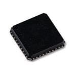
ICGOO电子元器件商城为您提供ADUC7021BCPZ32由Analog设计生产,在icgoo商城现货销售,并且可以通过原厂、代理商等渠道进行代购。 ADUC7021BCPZ32价格参考¥询价-¥询价。AnalogADUC7021BCPZ32封装/规格:嵌入式 - 微控制器, ARM7® 微控制器 IC MicroConverter® ADuC7xxx 16/32-位 44MHz 32KB(16K x 16) 闪存 40-LFCSP-VQ(6x6)。您可以下载ADUC7021BCPZ32参考资料、Datasheet数据手册功能说明书,资料中有ADUC7021BCPZ32 详细功能的应用电路图电压和使用方法及教程。
ADUC7021BCPZ32是由Analog Devices Inc.(亚德诺半导体公司)生产的一款嵌入式微控制器,属于ADuC702x系列。它是一款高性能、低功耗的32位ARM7TDMI微控制器,集成了丰富的模拟和数字外设,适用于多种工业、医疗和消费类应用场景。

 应用场景

1. 工业自动化与控制:
   ADUC7021BCPZ32在工业自动化领域有着广泛的应用。其内置的高精度ADC(模数转换器)可以用于实时监测传感器数据,如温度、压力、湿度等。通过集成的DAC(数模转换器),它可以精确控制执行器或电机的速度和位置。此外,该微控制器还支持多种通信接口(如UART、SPI、I²C),便于与其他设备进行通信,实现分布式控制系统。

2. 医疗设备:
   在医疗设备中,ADUC7021BCPZ32可以用于便携式医疗仪器的设计。例如,在血糖仪、心率监测仪等设备中,它可以通过内置的ADC采集生物信号,并通过DSP指令集进行快速处理。其低功耗特性使得电池供电的设备能够长时间工作,而不会频繁更换电池。此外,该微控制器还可以用于监控患者的生理参数,并通过无线通信模块将数据传输到远程服务器。

3. 智能家居与物联网:
   ADUC7021BCPZ32可用于智能家居系统中的各种传感器节点。例如,它可以用于环境监测系统,实时采集室内温湿度、光照强度等数据,并通过Wi-Fi或Zigbee等无线通信协议将数据上传到云端。由于其具备强大的计算能力和丰富的外设接口,它还可以用于智能门锁、智能照明等设备的控制逻辑处理。

4. 汽车电子:
   在汽车电子领域,ADUC7021BCPZ32可以用于车身控制系统、车载娱乐系统等。其高精度ADC和DAC可以用于传感器信号的采集和处理,而丰富的通信接口则可以用于与其他ECU(电子控制单元)进行通信。此外,该微控制器还可以用于汽车安全系统,如胎压监测、倒车雷达等。

5. 便携式测试设备:
   ADUC7021BCPZ32适用于便携式测试设备的设计。例如,在手持式示波器、频谱分析仪等设备中,它可以用于信号的高速采样和处理,并通过LCD显示屏实时显示结果。其内置的Flash存储器可以用于保存测量数据,方便后续分析。

总之,ADUC7021BCPZ32凭借其高性能、低功耗和丰富的外设接口,适用于多种需要精确模拟信号处理和高效数字控制的应用场景。
| 参数 | 数值 |
| A/D位大小 | 12 bit |
| 产品目录 | 集成电路 (IC)半导体 |
| 描述 | IC MCU ARM7 32KB FLASH 40LFCSPARM微控制器 - MCU Precision 1 MSPS 12-Bit Analog I/O |
| EEPROM容量 | - |
| 产品分类 | |
| I/O数 | 13 |
| 品牌 | Analog Devices |
| 产品手册 | |
| 产品图片 |
|
| rohs | 符合RoHS无铅 / 符合限制有害物质指令(RoHS)规范要求 |
| 产品系列 | 嵌入式处理器和控制器,微控制器 - MCU,ARM微控制器 - MCU,Analog Devices ADUC7021BCPZ32MicroConverter® ADuC7xxx |
| 数据手册 | |
| 产品型号 | ADUC7021BCPZ32 |
| PCN组件/产地 | |
| RAM容量 | 1K x 32 |
| 产品培训模块 | http://www.digikey.cn/PTM/IndividualPTM.page?site=cn&lang=zhs&ptm=3452http://www.digikey.cn/PTM/IndividualPTM.page?site=cn&lang=zhs&ptm=3052 |
| 产品种类 | ARM微控制器 - MCU |
| 供应商器件封装 | 40-LFCSP-VQ(6x6) |
| 包装 | 托盘 |
| 可用A/D通道 | 8 |
| 可编程输入/输出端数量 | 13 |
| 商标 | Analog Devices |
| 处理器系列 | ARM7 |
| 外设 | PLA,PWM,PSM,温度传感器,WDT |
| 安装风格 | SMD/SMT |
| 定时器数量 | 4 Timer |
| 封装 | Tray |
| 封装/外壳 | 40-VFQFN 裸露焊盘,CSP |
| 封装/箱体 | LFCSP-40 |
| 工作温度 | -40°C ~ 125°C |
| 工厂包装数量 | 490 |
| 振荡器类型 | 内部 |
| 接口类型 | I2C/SPI/UART |
| 数据RAM大小 | 8192 B |
| 数据总线宽度 | 16 bit/32 bit |
| 数据转换器 | A/D 8x12b,D/A 2x12b |
| 最大工作温度 | + 85 C |
| 最大时钟频率 | 40 MHz |
| 最小工作温度 | - 40 C |
| 标准包装 | 1 |
| 核心 | ARM7TDMI |
| 核心处理器 | ARM7® |
| 核心尺寸 | 16/32-位 |
| 片上ADC | Yes |
| 片上DAC | With DAC |
| 电压-电源(Vcc/Vdd) | 2.7 V ~ 3.6 V |
| 程序存储器大小 | 32 kB |
| 程序存储器类型 | Flash |
| 程序存储容量 | 32KB(16K x 16) |
| 系列 | ADUC7021 |
| 输入/输出端数量 | 13 I/O |
| 连接性 | EBI/EMI, I²C, SPI, UART/USART |
| 速度 | 44MHz |
| 长度 | 6 mm |


- 商务部:美国ITC正式对集成电路等产品启动337调查
- 曝三星4nm工艺存在良率问题 高通将骁龙8 Gen1或转产台积电
- 太阳诱电将投资9.5亿元在常州建新厂生产MLCC 预计2023年完工
- 英特尔发布欧洲新工厂建设计划 深化IDM 2.0 战略
- 台积电先进制程称霸业界 有大客户加持明年业绩稳了
- 达到5530亿美元!SIA预计今年全球半导体销售额将创下新高
- 英特尔拟将自动驾驶子公司Mobileye上市 估值或超500亿美元
- 三星加码芯片和SET,合并消费电子和移动部门,撤换高东真等 CEO
- 三星电子宣布重大人事变动 还合并消费电子和移动部门
- 海关总署:前11个月进口集成电路产品价值2.52万亿元 增长14.8%


PDF Datasheet 数据手册内容提取
Precision Analog Microcontroller, 12-Bit Analog I/O, ARM7TDMI MCU with Enhanced IRQ Handler Data Sheet ADuC7023 FEATURES APPLICATIONS Analog I/O Optical networking Multichannel, 12-bit, 1 MSPS ADC Industrial control and automation systems Up to 12 ADC channels Smart sensors, precision instrumentation Fully differential and single-ended modes Base station systems 0 V to V analog input range REF GENERAL DESCRIPTION 12-bit voltage output DACs 4 DAC outputs available The ADuC7023 is a fully integrated, 1 MSPS, 12-bit data acquisition On-chip voltage reference system, incorporating high performance multichannel ADCs, On-chip temperature sensor 16-bit/32-bit MCUs, and Flash/EE memory on a single chip. Voltage comparator The ADC consists of up to 12 single-ended inputs. An additional four Microcontroller inputs are available but are multiplexed with the four DAC output ARM7TDMI core, 16-bit/32-bit RISC architecture pins. The ADC can operate in single-ended or differential input modes. JTAG port supports code download and debug The ADC input voltage is 0 V to V . A low drift band gap reference, REF Clocking options temperature sensor, and voltage comparator complete the ADC Trimmed on-chip oscillator (±3%) peripheral set. External watch crystal The DAC output range is programmable to one of two voltage ranges. External clock source up to 44 MHz The DAC outputs have an enhanced feature of being able to retain 41.78 MHz PLL with programmable divider their output voltage during a watchdog or software reset sequence. Memory The devices operate from an on-chip oscillator and a PLL, generating 62 kB Flash/EE memory, 8 kB SRAM an internal high frequency clock of 41.78 MHz. This clock is routed In-circuit download, JTAG-based debug through a programmable clock divider from which the MCU core Software-triggered in-circuit reprogrammability clock operating frequency is generated. The microcontroller core is an Vectored interrupt controller for FIQ and IRQ ARM7TDMI®, 16-bit/32-bit RISC machine that offers up to 41 MIPS 8 priority levels for each interrupt type peak performance. Eight kilobytes of SRAM and 62 kilobytes of Interrupt on edge or level external pin inputs nonvolatile Flash/EE memory are provided on chip. The ARM7TDMI On-chip peripherals core views all memory and registers as a single linear array. 2× fully I2C-compatible channels The ADuC7023 contains an advanced interrupt controller. The SPI (20 Mbps in master mode, 10 Mbps in slave mode) vectored interrupt controller (VIC) allows every interrupt to be With 4-byte FIFO on input and output stages assigned a priority level. It also supports nested interrupts to a Up to 20 GPIO pins—Digital only GPIOs are 5 V tolerant maximum level of eight per IRQ and FIQ. When IRQ and FIQ 3× general-purpose timers interrupt sources are combined, a total of 16 nested interrupt Watchdog timer (WDT) levels are supported. Programmable logic array (PLA) On-chip factory firmware supports in-circuit download via the I2C 16 PLA elements serial interface port, and nonintrusive emulation is supported via 16-bit, 5-channel PWM the JTAG interface. These features are incorporated into a low cost Power QuickStart™ development system supporting this MicroConverter® Specified for 3 V operation family. The part contains a 16-bit PWM with five output signals. Active mode: 11 mA at 5 MHz, 28 mA at 41.78 MHz For communication purposes, the part contains 2 × I2C channels that Packages and temperature range can be individually configured for master or slave mode. An SPI 32-lead 5 mm × 5 mm LFCSP interface supporting both master and slave modes is also provided. 40-lead LFCSP 36-Lead WLCSP The parts operate from 2.7 V to 3.6 V and are specified over an Fully specified for −40°C to +125°C operation industrial temperature range of −40°C to +125°C. The ADuC7023 is Tools available in either a 32-lead or 40-lead LFCSP package. A 36-ball Low cost QuickStart development system wafer level CSP package (WLCSP) is also available. Full third-party support Rev. G Document Feedback Information furnished by Analog Devices is believed to be accurate and reliable. However, no responsibility is assumed by Analog Devices for its use, nor for any infringements of patents or other One Technology Way, P.O. Box 9106, Norwood, MA 02062-9106, U.S.A. rights of third parties that may result from its use. Specifications subject to change without notice. No license is granted by implication or otherwise under any patent or patent rights of Analog Devices. Tel: 781.329.4700 ©2010–2015 Analog Devices, Inc. All rights reserved. Trademarks and registered trademarks are the property of their respective owners. Technical Support www.analog.com
ADuC7023 Data Sheet TABLE OF CONTENTS Features .............................................................................................. 1 Security ........................................................................................ 39 Applications ....................................................................................... 1 Flash/EE Control Interface ....................................................... 39 General Description ......................................................................... 1 Execution Time from SRAM and Flash/EE ............................ 42 Revision History ............................................................................... 3 Reset and Remap ........................................................................ 42 Functional Block Diagram .............................................................. 5 Other Analog Peripherals .............................................................. 45 Specifications ..................................................................................... 6 DAC .............................................................................................. 45 Timing Specifications .................................................................. 9 Power Supply Monitor ............................................................... 47 Absolute Maximum Ratings .......................................................... 14 Comparator ................................................................................. 47 ESD Caution ................................................................................ 14 Oscillator and PLL—Power Control ........................................ 49 Pin Configurations and Function Descriptions ......................... 15 Digital Peripherals .......................................................................... 52 Typical Performance Characteristics ........................................... 19 General-Purpose Input/Output................................................ 52 Terminology .................................................................................... 20 Serial Peripheral Interface ......................................................... 55 ADC Specifications .................................................................... 20 I2C ..................................................................................................... 60 DAC Specifications..................................................................... 20 Configuring External Pins for I2C Functionality ................... 60 Overview of the ARM7TDMI Core ............................................. 21 Serial Clock Generation ............................................................ 60 Thumb Mode (T) ........................................................................ 21 I2C Bus Addresses ....................................................................... 60 Long Multiply (M) ...................................................................... 21 I2C Registers ................................................................................ 61 EmbeddedICE (I) ....................................................................... 21 Programmable Logic Array (PLA)........................................... 68 Exceptions ................................................................................... 21 Pulse-Width Modulator ................................................................. 72 ARM Registers ............................................................................ 21 Pulse-Width Modulator General Overview ........................... 72 Interrupt Latency ........................................................................ 22 Processor Reference Peripherals ................................................... 77 Memory Organization ................................................................... 23 Interrupt System ......................................................................... 77 Memory Access ........................................................................... 23 IRQ ............................................................................................... 77 Flash/EE Memory ....................................................................... 23 Fast Interrupt Request (FIQ) .................................................... 78 SRAM ........................................................................................... 23 Vectored Interrupt Controller (VIC) ....................................... 79 Memory Mapped Registers ....................................................... 23 Timers .......................................................................................... 84 ADC Circuit Overview .................................................................. 30 Hardware Design Considerations ................................................... 89 Transfer Function ....................................................................... 30 Power Supplies ............................................................................. 89 Typical Operation ....................................................................... 31 Grounding and Board Layout Recommendations ................. 90 MMR Interface ............................................................................ 31 Clock Oscillator .......................................................................... 90 Converter Operation .................................................................. 34 Power-On Reset Operation ....................................................... 91 Driving the Analog Inputs ........................................................ 35 Typical System Configuration .................................................. 92 Calibration ................................................................................... 35 Development Tools......................................................................... 93 Temperature Sensor ................................................................... 35 PC-Based Tools ........................................................................... 93 Band Gap Reference ................................................................... 37 In-Circuit I2C Downloader ....................................................... 93 Nonvolatile Flash/EE Memory ..................................................... 38 Outline Dimensions ....................................................................... 94 Programming .............................................................................. 38 Ordering Guide .......................................................................... 96 Rev. G | Page 2 of 97
Data Sheet ADuC7023 REVISION HISTORY 1/15—Rev. F to Rev. G 5/12—Rev. B to Rev. C Changes to Table 53 ........................................................................ 51 Changed SDATA to SDA and SCLK to SCL, Table 2; SDATA to Changes to I2C Section ................................................................... 60 SDA and SCLK to SCL, Table 3; and SDATA to SDA and SCLK Changes to Table 65 ........................................................................ 61 to SCL, Figure 2 ................................................................................. 8 Changes to Table 72 ........................................................................ 64 Changes to Figure 7, Figure 8, and Table 9 .................................. 14 Changes to I2CREPS Bit Description, Table 73 .......................... 66 Changed SCLK to SCL, Table 17 ................................................... 25 Changed SCLK to SCL, Table 18 ................................................... 26 5/14—Rev. E to Rev. F Changes to Bit 6, Table 24 and 4 to 0, Description Column, Change CONVSTART Pin to CONVSTART Pin ................ Throughout Table 25 ............................................................................................. 30 Change to Layout, Power Requirements Parameter, Table 1 ....... 7 Changed Reference in REFCON Register Section from Table 22 Change to Table 8 ............................................................................ 13 to Table 30 ........................................................................................ 35 Changes to Figure 7 and Table 9 ................................................... 14 Added Note 1 to Table 53 ............................................................... 49 Change to Table 21 .......................................................................... 28 Changes to Note 1, Table 55........................................................... 50 Change to Figure 23 ........................................................................ 30 Changed SPICLK (Serial Clock I/O) Pin Section to SCLK Change to JTAG Access Section .................................................... 37 (Serial Clock I/O) Pin Section ....................................................... 53 Changes to Table 36 ........................................................................ 42 Changed SPICLK to SCLK in Serial Peripheral Interface Section Changes to Table 55 ........................................................................ 51 and in SCLK (Serial Clock I/O) Pin Section ............................... 53 Changes to I2C Bus Addresses Section ......................................... 59 Changes to Table 79 ........................................................................ 68 Change to Table 84 .......................................................................... 71 Changes to Timers Section ............................................................ 82 Added PWM2LEN Register Section............................................. 75 Added Hours, Minutes, Seconds, and 1/128 Format Section and Table 101 ........................................................................................... 82 7/13—Rev. D to Rev. E Changes to T0LD Register Section and T1LD Register Section ..... 83 Changes to Ordering Guide ........................................................... 95 Changes to T2LD Register Section......................................................... 85 Updated Outline Dimensions........................................................ 92 7/13—Rev. C to Rev. D Changes to Ordering Guide ........................................................... 93 Added WLCSP (Throughout) ......................................................... 1 Changes to Features Section ............................................................ 1 7/10—Rev. A to Rev. B Added Shared Analog/Digital Inputs to AGND Rating of −0.3 V Changes to Temperature Sensor Parameter in Table 1 ................ 6 to AV + 0.3 V, Endnote 1, and Endnote 2; Table 8 .................. 13 Change to Table 10 and changes to Table 11 ............................... 23 DD Added Figure 9; Renumbered Sequentially; Added WLCSP Pin Changes to Table 12 and Table 13 ................................................. 24 Numbers to Table 9 ......................................................................... 14 Changes to Table 16 and Table 17 ................................................. 25 Changes to Pin P1.7/PWM3/SDA1/PLAI[6] and Pin Changes to Table 18 ........................................................................ 26 P1.6/PWM2/SCL1/PLAI[5] Descriptions; Table 9 ..................... 16 Change to Table 21 and changes to Table 22 ............................... 27 Changes to ADC Circuit Overview Section, Transfer Function Changes to Table 24 ........................................................................ 29 Section, and Figure 20 Caption ..................................................... 29 Changes to ADCGN Register and ADCOF Register Sections . 32 Changes to Typical Operation Section, ADCCON Register Changes to Temperature Sensor Section ..................................... 34 Section, and ADCON[13] Description in Table 24 .................... 30 Changes to Table 29 ........................................................................ 35 Changes to Bits[4:3] Value 10 Description; Table 24.................. 31 Change to REMAP Register and RSTCLR Register Sections ... 41 Changes to Converter Operation Section and Deleted Pseudo Change to RSTKEY1 Register and RSTKEY2 Register Differential Mode Section .............................................................. 33 Sections ............................................................................................. 42 Changes to Figure 27 and Figure 28 Caption .............................. 34 Changes to Oscillator and PLL—Power Control Section .......... 48 Changes to Table 30 and Following Text ...................................... 36 Changes to General-Purpose Input/Output Section .................. 51 Changes to JTAG Access Section .................................................. 37 Changes to Serial Peripheral Interface Section ........................... 53 Changes to References to ADC and the DACs Section ............. 45 Changes to Table 75 ........................................................................ 67 Changes to General-Purpose Input/Output Section .................. 51 Changes to Table 83 and Pulse-Width Modulator General Changes to SPIDIV Register Section ............................................ 56 Overview Section ............................................................................ 70 Changes to Bits[1:0] Value 01 Description; Table 66.................. 61 Changes to Table 84 ........................................................................ 71 Changes to T0CLRI Register Section ........................................... 84 Change to Table 85 .......................................................................... 72 Changes to Figure 53 ...................................................................... 90 Change to FIQSTAN Register Section ......................................... 81 Updated Outline Dimensions ........................................................ 93 Change to T2CLRI Register Section ............................................. 85 Changes to Ordering Guide ........................................................... 95 Rev. G | Page 3 of 97
ADuC7023 Data Sheet 6/10—Rev. 0 to Rev. A 1/10—Revision 0: Initial Version Changes to Temperature Sensor Parameter in Table 1 ................ 6 Changes to Table 24 ........................................................................ 29 Changes to Temperature Sensor Section ..................................... 34 Changes to DACBKEY0 Register Section and to Table 43 ....... 47 Changes to Ordering Guide .......................................................... 93 Rev. G | Page 4 of 97
Data Sheet ADuC7023 FUNCTIONAL BLOCK DIAGRAM ADC0 12-BIT DAC0 DAC 1MSPS ADuC7023 MUX 12-BIT ADC 40-LEAD LFCSP 12-BIT ADC12 DAC1 DAC TEMP SENSOR 12-BIT DAC2 ADC2/CMP0 DAC ADC3/CMP1 BANRDE FGAP IVNETCETRORRUEPDT 1D2-ABCIT DAC3 CMPOUT CONTROLLER VREF OSC ARM7TDMI-BASED MCU WITH XCLKI AND PLL ADDITIONAL PERIPHERALS XCLKO 2k × 32 SRAM PLA GPIO PSM 31k × 16 FLASH/EEPROM PWM RST POR PUR3 PGOESNEE RTIAMLE-RS SPI, 2 × I2C JTAG 08675-001 Figure 1. Rev. G | Page 5 of 97
ADuC7023 Data Sheet SPECIFICATIONS AV = IOV = 2.7 V to 3.6 V, V = 2.5 V internal reference, f = 41.78 MHz, T = −40°C to +125°C, unless otherwise noted. DD DD REF CORE A Table 1. Parameter Min Typ Max Unit Test Conditions/Comments ADC CHANNEL SPECIFICATIONS Eight acquisition clocks and fADC/2 ADC Power-Up Time 5 μs DC Accuracy1, 2 Resolution 12 Bits Integral Nonlinearity ±0.6 ±1.5 LSB 2.5 V internal reference ±1.0 LSB 1.0 V external reference Differential Nonlinearity3, 4 ±0.5 +1/−0.9 LSB 2.5 V internal reference +0.7/−0.6 LSB 1.0 V external reference DC Code Distribution 1 LSB ADC input is a dc voltage ENDPOINT ERRORS5 Offset Error ±1 ±2 LSB Offset Error Match ±1 LSB Gain Error ±2 LSB Gain Error Match ±1 LSB DYNAMIC PERFORMANCE fIN = 10 kHz sine wave, fSAMPLE = 1 MSPS Signal-to-Noise Ratio (SNR) 69 dB Includes distortion and noise components Total Harmonic Distortion (THD) −78 dB Peak Harmonic or Spurious Noise −75 dB Channel-to-Channel Crosstalk −80 dB Measured on adjacent channels ANALOG INPUT Input Voltage Ranges Differential Mode VCM ± VREF/26 V Single-Ended Mode 0 to VREF V Leakage Current ±1 ±6 µA Input Capacitance 20 pF During ADC acquisition ON-CHIP VOLTAGE REFERENCE 0.47 µF from VREF to AGND Output Voltage 2.5 V Accuracy ±4 mV TA = 25°C Reference Temperature Coefficient ±15 ppm/°C Power Supply Rejection Ratio 75 dB Output Impedance 51 Ω TA = 25°C Internal VREF Power-On Time 1 ms EXTERNAL REFERENCE INPUT Input Voltage Range 0.625 AVDD V DAC CHANNEL SPECIFICATIONS DC Accuracy7 RL = 5 kΩ, CL = 100 pF Resolution 12 Bits Relative Accuracy ±2 LSB Differential Nonlinearity ±1 LSB Guaranteed monotonic Offset Error ±15 mV 2.5 V internal reference Gain Error8 ±1 % Gain Error Mismatch 0.1 % % of full scale on DAC0 DC Accuracy9 RL = 1 kΩ, CL = 100 pF Resolution 12 Bits Relative Accuracy ±2.5 LSB Differential Nonlinearity ±1 LSB Guaranteed monotonic Offset Error ±15 mV 2.5 V internal reference Gain Error10 ±1 % Gain Error Mismatch 0.1 % % of full scale on DAC0 ANALOG OUTPUTS Output Voltage Range 1 0 to 2.5 V VREF range: AGND to AVDD Output Voltage Range 2 0 to AVDD V Output Impedance 2 Ω Rev. G | Page 6 of 97
Data Sheet ADuC7023 Parameter Min Typ Max Unit Test Conditions/Comments DAC IN OP AMP MODE DAC Output Buffer in Op Amp Mode Input Offset Voltage ±0.25 mV Input Offset Voltage Drift 8 µV/°C Input Offset Current 0.3 nA Input Bias Current 0.4 nA Gain 80 dB 5 kΩ load Unity-Gain Frequency 5 MHz RL = 5 kΩ, CL = 100 pF CMRR 80 dB Settling Time 10 µs RL = 5 kΩ, CL = 100 pF Output Slew Rate 1.5 V/µs RL = 5 kΩ, CL = 100 pF PSRR 75 dB DAC AC CHARACTERISTICS Voltage Output Settling Time 10 µs Digital-to-Analog Glitch Energy ±20 nV-sec 1 LSB change at major carry (where maximum number of bits simultaneously change in the DACxDAT register) COMPARATOR Input Offset Voltage ±10 mV Input Bias Current 1 µA Input Voltage Range AGND AVDD – 1.2 V Input Capacitance 7 pF Hysteresis4, 6 2 15 mV Hysteresis can be turned on or off via the CMPHYST bit in the CMPCON register Response Time 3 µs 100 mV overdrive and configured with CMPRES = 11 TEMPERATURE SENSOR Indicates die temperature Voltage Output at 25°C 1.369 V Voltage TC 4.42 mV/°C Accuracy with No Calibration ±3 °C Accuracy with One Point Calibration ±1.5 °C Using Contents of TEMPREF Register θJA Thermal Impedance 40-Lead LFCSP 26 °C/W 32-Lead LFCSP 32.5 °C/W POWER SUPPLY MONITOR (PSM) IOVDD Trip Point Selection 2.79 V One trip point Power Supply Trip Point Accuracy ±2 % Of the selected nominal trip point voltage POWER-ON RESET 2.41 V WATCHDOG TIMER (WDT) Timeout Period 0 512 sec FLASH/EE MEMORY Endurance11 10,000 Cycles Data Retention12 20 Years TJ = 85°C DIGITAL INPUTS All digital inputs excluding XCLKI and XCLKO Logic 1 Input Current ±0.2 ±1 µA VIH = VDD or VIH = 5 V Logic 0 Input Current −40 −60 µA VIL = 0 V; except TDI −80 −120 µA VIL = 0 V; TDI Input Capacitance 10 pF LOGIC INPUTS4 All logic inputs excluding XCLKI VINL, Input Low Voltage 0.8 V VINH, Input High Voltage 2.0 V LOGIC OUTPUTS All digital outputs excluding XCLKO VOH, Output High Voltage 2.4 V ISOURCE = 1.6 mA VOL, Output Low Voltage13 0.4 V ISINK = 1.6 mA CRYSTAL INPUTS XCLKI AND XCLKO Logic Inputs, XCLKI Only VINL, Input Low Voltage 1.1 V VINH, Input High Voltage 1.7 V XCLKI Input Capacitance 20 pF XCLKO Output Capacitance 20 pF Rev. G | Page 7 of 97
ADuC7023 Data Sheet Parameter Min Typ Max Unit Test Conditions/Comments INTERNAL OSCILLATOR 32.768 kHz ±3 % MCU CLOCK RATE From 32 kHz Internal Oscillator 326 kHz CD = 7 From 32 kHz External Crystal 41.78 MHz CD = 0 Using an External Clock 0.05 44 MHz TA = 85°C 0.05 41.78 MHz TA = 125°C START-UP TIME Core clock = 41.78 MHz At Power-On 66 ms From Pause/Nap Mode 24 ns CD = 0 3.07 µs CD = 7 From Sleep Mode 1.58 ms From Stop Mode 1.7 ms PROGRAMMABLE LOGIC ARRAY (PLA) Pin Propagation Delay 12 ns From input pin to output pin Element Propagation Delay 2.5 ns POWER REQUIREMENTS14, 15 Power Supply Voltage Range AVDD to AGND and IOVDD to DGND 2.7 3.6 V Analog Power Supply Currents AVDD Current 200 µA ADC in idle mode Digital Power Supply Current IOVDD Current in Normal Mode Code executing from Flash/EE 8.5 10 mA CD = 7 11 15 mA CD = 3 28 35 mA CD = 0 (41.78 MHz clock) IOVDD Current in Pause Mode 14 20 mA CD = 0 (41.78 MHz clock) IOVDD Current in Sleep Mode 230 650 µA TA = 125°C Additional Power Supply Currents ADC 1.4 mA At 1 MSPS 0.7 mA At 62.5 kSPS DAC 400 µA Per DAC ESD TESTS 2.5 V reference, TA = 25°C HBM Passed 3 kV FICDM Passed 1.0 kV 1 All ADC channel specifications are guaranteed during normal microcontroller core operation. 2 Apply to all ADC input channels. 3 Measured using the factory-set default values in the ADC offset register (ADCOF) and gain coefficient register (ADCGN). 4 Not production tested but supported by design and/or characterization data on production release. 5 Measured using the factory-set default values in ADCOF and ADCGN with an external AD845 op amp as an input buffer stage as shown in Figure 28. Based on external ADC system components, the user may need to execute a system calibration to remove external endpoint errors and achieve these specifications (see the Calibration section). 6 The input signal can be centered on any dc common-mode voltage (VCM) as long as this value is within the ADC voltage input range specified. 7 DAC linearity is calculated using a reduced code range of 100 to 3995. 8 DAC gain error is calculated using a reduced code range of 100 to internal 2.5 V VREF. 9 DAC linearity is calculated using a reduced code range of 100 to 3995. 10 DAC gain error is calculated using a reduced code range of 100 to internal 2.5 V VREF. 11 Endurance is qualified as per JEDEC Standard 22 Method A117 and measured at −40°C, +25°C, +85°C, and +125°C. 12 Retention lifetime equivalent at junction temperature (TJ) = 85°C as per JEDEC Standard 22 Method A117. Retention lifetime derates with junction temperature. 13 Test carried out with a maximum of eight I/Os set to a low output level. 14 Power supply current consumption is measured in normal, pause, and sleep modes under the following conditions: normal mode with 3.6 V supply, pause mode with 3.6 V supply, and sleep mode with 3.6 V supply. 15 IOVDD power supply current decreases typically by 2 mA during a Flash/EE erase cycle. Rev. G | Page 8 of 97
Data Sheet ADuC7023 TIMING SPECIFICATIONS Table 2. I2C Timing in Fast Mode (400 kHz) Slave Master Parameter Description Min Max Typ Unit t SCL low pulse width 200 1360 ns L t SCL high pulse width 100 1140 ns H t Start condition hold time 300 ns SHD t Data setup time 100 740 ns DSU t Data hold time 0 400 ns DHD t Setup time for repeated start 100 ns RSU t Stop condition setup time 100 800 ns PSU t Bus-free time between a stop condition and a start condition 1.3 µs BUF t Rise time for both SCL and SDA 300 200 ns R t Fall time for both SCL and SDA 300 ns F Table 3. I2C Timing in Standard Mode (100 kHz) Slave Parameter Description Min Max Unit t SCL low pulse width 4.7 µs L t SCL high pulse width 4.0 ns H t Start condition hold time 4.0 µs SHD t Data setup time 250 ns DSU t Data hold time 0 3.45 µs DHD t Setup time for repeated start 4.7 µs RSU t Stop condition setup time 4.0 µs PSU t Bus-free time between a stop condition and a start condition 4.7 µs BUF t Rise time for both SCL and SDA 1 µs R t Fall time for both SCL and SDA 300 ns F tBUF tSUP tR SDA(I/O) MSB LSB ACK MSB tDSU tDSU tF tPSU tDHD tDHD tSHD tH tRSU tR SCL (I) 1 2–7 8 9 1 COSNTDOIPTPION COSNTSDAIRTITON tL tSUP RESPSTEA(RAR)TTED tF 08675-002 Figure 2. I2C-Compatible Interface Timing Rev. G | Page 9 of 97
ADuC7023 Data Sheet Table 4. SPI Master Mode Timing (Phase Mode = 1) Parameter Description Min Typ Max Unit t SCLK low pulse width1 (SPIDIV + 1) × t ns SL UCLK t SCLK high pulse width1 (SPIDIV + 1) × t ns SH UCLK t Data output valid after SCLK edge 25 ns DAV t Data input setup time before SCLK edge1 1 × t ns DSU UCLK t Data input hold time after SCLK edge1 2 × t ns DHD UCLK t Data output fall time 5 12.5 ns DF t Data output rise time 5 12.5 ns DR t SCLK rise time 5 12.5 ns SR t SCLK fall time 5 12.5 ns SF 1 tUCLK = 23.9 ns. It corresponds to the 41.78 MHz internal clock from the PLL before the clock divider. SCLK (POLARITY=0) tSH tSL tSR tSF SCLK (POLARITY=1) tDAV tDF tDR MOSI MSB BIT6TOBIT 1 LSB MISO MSB IN BIT 6TOBIT 1 LSB IN tDSU tDHD 08675-003 Figure 3. SPI Master Mode Timing (Phase Mode = 1) Rev. G | Page 10 of 97
Data Sheet ADuC7023 Table 5. SPI Master Mode Timing (Phase Mode = 0) Parameter Description Min Typ Max Unit t SCLK low pulse width1 (SPIDIV + 1) × t ns SL UCLK t SCLK high pulse width1 (SPIDIV + 1) × t ns SH UCLK t Data output valid after SCLK edge 25 ns DAV t Data output setup before SCLK edge 75 ns DOSU t Data input setup time before SCLK edge1 1 × t ns DSU UCLK t Data input hold time after SCLK edge1 2 × t ns DHD UCLK t Data output fall time 5 12.5 ns DF t Data output rise time 5 12.5 ns DR t SCLK rise time 5 12.5 ns SR t SCLK fall time 5 12.5 ns SF 1 tUCLK = 23.9 ns. It corresponds to the 41.78 MHz internal clock from the PLL before the clock divider. SCLK (POLARITY=0) tSH tSL tSR tSF SCLK (POLARITY=1) tDAV tDOSU tDF tDR MOSI MSB BIT 6TOBIT 1 LSB MISO MSB IN BIT6TOBIT 1 LSB IN tDSU tDHD 08675-004 Figure 4. SPI Master Mode Timing (Phase Mode = 0) Rev. G | Page 11 of 97
ADuC7023 Data Sheet Table 6. SPI Slave Mode Timing (Phase Mode = 1) Parameter Description Min Typ Max Unit t SS to SCLK edge 200 ns SS t SCLK low pulse width1 (SPIDIV + 1) × t ns SL UCLK t SCLK high pulse width1 (SPIDIV + 1) × t ns SH UCLK t Data output valid after SCLK edge 25 ns DAV t Data input setup time before SCLK edge1 1 × t ns DSU UCLK t Data input hold time after SCLK edge1 2 × t ns DHD UCLK t Data output fall time 5 12.5 ns DF t Data output rise time 5 12.5 ns DR t SCLK rise time 5 12.5 ns SR t SCLK fall time 5 12.5 ns SF tSFS SS high after SCLK edge 0 ns 1 tUCLK = 23.9 ns. It corresponds to the 41.78 MHz internal clock from the PLL before the clock divider. SS tSS tSFS SCLK (POLARITY=0) tSH tSL tSR tSF SCLK (POLARITY=1) tDAV tDF tDR MOSI MSB BIT6TOBIT 1 LSB MISO MSB IN BIT6TOBIT 1 LSB IN tDSU tDHD 08675-005 Figure 5. SPI Slave Mode Timing (Phase Mode = 1) Rev. G | Page 12 of 97
Data Sheet ADuC7023 Table 7. SPI Slave Mode Timing (Phase Mode = 0) Parameter Description Min Typ Max Unit t SS to SCLK edge 200 ns SS t SCLK low pulse width1 (SPIDIV + 1) × t ns SL UCLK t SCLK high pulse width1 (SPIDIV + 1) × t ns SH UCLK t Data output valid after SCLK edge 25 ns DAV t Data input setup time before SCLK edge1 1 × t ns DSU UCLK t Data input hold time after SCLK edge1 2 × t ns DHD UCLK t Data output fall time 5 12.5 ns DF t Data output rise time 5 12.5 ns DR t SCLK rise time 5 12.5 ns SR t SCLK fall time 5 12.5 ns SF tDOCS Data output valid after SS edge 25 ns tSFS SS high after SCLK edge 0 ns 1 tUCLK = 23.9 ns. It corresponds to the 41.78 MHz internal clock from the PLL before the clock divider. SS tSS tSFS SCLK (POLARITY=0) tSH tSL tSR tSF SCLK (POLARITY=1) tDAV tDOCS tDF tDR MOSI MSB BIT6TOBIT 1 LSB MISO MSB IN BIT6TO BIT1 LSB IN tDSU tDHD 08675-006 Figure 6. SPI Slave Mode Timing (Phase Mode = 0) Rev. G | Page 13 of 97
ADuC7023 Data Sheet ABSOLUTE MAXIMUM RATINGS AGND = GND , T = 25°C, unless otherwise noted. REF A Table 8. Stresses at or above those listed under Absolute Maximum Parameter Rating Ratings may cause permanent damage to the product. This is a AV to IOV −0.3 V to +0.3 V stress rating only; functional operation of the product at these DD DD AGND to DGND −0.3 V to +0.3 V or any other conditions above those indicated in the operational IOV to DGND, AV to AGND −0.3 V to +6 V section of this specification is not implied. Operation beyond DD DD Digital Input Voltage to DGND1 −0.3 V to +5.3 V the maximum operating conditions for extended periods may Digital Output Voltage to DGND1 −0.3 V to IOV + 0.3 V affect product reliability. DD Shared Analog/Digital Inputs to AGND2 −0.3 V to AV + 0.3 V DD Only one absolute maximum rating can be applied at any one time. V to AGND −0.3 V to AV + 0.3 V REF DD Analog Inputs to AGND −0.3 V to AVDD + 0.3 V Analog Outputs to AGND −0.3 V to AV + 0.3 V ESD CAUTION DD Operating Temperature Range, Industrial −40°C to +125°C Storage Temperature Range −65°C to +150°C Junction Temperature 150°C θ Thermal Impedance JA 40-Lead LFCSP 26°C/W 32-Lead LFCSP 32.5°C/W 36-Lead WLCSP 50°C/W Peak Solder Reflow Temperature SnPb Assemblies (10 sec to 30 sec) 240°C RoHS Compliant Assemblies 260°C (20 sec to 40 sec) 1 These limits apply to the P0.0, P0.1, P0.2, P0.3, P0.4, P0.5, P0.6, P0.7, P1.0, P1.1, P1.6, and P1.7 pins. 2 These limits apply to the P1.2, P1.3, P1.4, P1.5, P2.0, P2.2, P2.3, and P2.4 pins. Rev. G | Page 14 of 97
Data Sheet ADuC7023 PIN CONFIGURATIONS AND FUNCTION DESCRIPTIONS K D0N4GA1PMC/3CDA930PMC/2CDA831CDA730CDA63V53FER]4[IALP/3QR/I5CDA/3.1P43KLCE/]3[AILP/2QRI/4CDA332/1.P]01[IALP/9CD2A3/4.2P7][OALP/8CDA13/32.P DNGA321PMC31/3CDA0PMC2/CDA301CDA290CDA28V27FER26]4[IALP3/QRI/5CDA/3.1P25LCE/3]I[ALP/2QR/I4CDA/2.1P GNDADAVRCDED0F 123 223890PPP012...352///PAALDDACCO67//[PS9WY]/NTMCCTK/RPILPAINOPU[6T]/PLAO[4] GNDADAVRCDED0F 123 ADuC7023 222432PPP000...321///PPPLLLAAAOOI[9[[98]/]]T//TTDCDOKI DDDAAACCC123 456 ATDOuPC V7IE0W23 222567PPP000...012///nPPTLLRAASIO[T9[8]//A]T/DTDDCOIBUSYPLAI[8]/BM DDDAAACCC123 456 (NToOt Pto V SIEcWale) 221109 PTRM0T.CS0K/nTRST/ADCBUSY/PLAI[8]/BM P0.4/IRQ0P/S2C.0L/A0P/DP1CL.41A/2AI[/DP0]WC/C1MO04/NP/PVLLSAATOAI[[R37T]] 789 (Not to Scale) 222342RTXMCTCLSKKO P0.4/IRQP00./5S/CSLD0A/P0/LPALIA[0I[]1/C]/OCNOVMSPTAORUTT 78 1187 XXCCLLKKOI P0.5/SDA0/PLAI[1]/COMPOUT10 21XCLKI 910111213141516 N1 . O EETXIETPHSOESRE CDOPNANDE. CTTHEEDP2]I[ALPO/SMI/6.0PTA11OD0]O[ALPI/SOM/7.0P21DA]1[OALP/0MWP/KLCILPS/0.1PG31ENIT/]2[OALP/1MWP1/QRIS/S1/.1P 41NDE ]5[AILP/1LCS/2MWP/6.1P51OER]6I[ALP1/ADS/3MWP7/1.PD61 SLDNGD71ETFVOIO81DDT VLB 91FDDEL02TSR OSAOTLIDNEGR.EDAND 08675-048 N1 . O EETXIETPHSOESRE CDOPNANDE. CTTHEED]2[IALP/1LCS/OSIM/6.0PPTA]0[OALP/1ADS/SIOM/7.0PODDA]1[OALP0/MWPK/LCIPS/0.1PLGE1T/2][OALP/1MWP/1QR/ISS/1.1PN NDDNGDE OEVOIRDDD SLVLDDETFOTSRT B FEL OSAOTLIDNEGR.EDAND 08675-007 Figure 8. 32-Lead LFCSP Pin Configuration Figure 7. 40-Lead LFCSP Pin Configuration BALLA1 CORNER 1 2 3 4 5 6 A A1 A2 A3 A4 A5 A6 B B1 B2 B3 B4 B5 B6 C C1 C2 C3 C4 C5 C6 D D1 D2 D3 D4 D5 D6 E E1 E2 E3 E4 E5 E6 F F1 F2 F3 F4 F5 F6 ADuC7023 (BALNTLoO tS PtIoD V ESIE cDWaOleWN) 08675-109 Figure 9. 36-Lead WLCSP Pin Configuration Table 9. Pin Function Descriptions Pin No. 40- 32- 36- LFCSP LFCSP WLCSP Mnemonic Description 0 0 N/A Exposed Paddle Exposed Pad. The paddle needs to be soldered and either connected to AGND or left floating. 36 28 A4 ADC0 Single-Ended or Differential Analog Input 0. 37 29 B4 ADC1 Single-Ended or Differential Analog Input 1. 38 30 A5 ADC2/CMP0 Single-Ended or Differential Analog Input 2/Comparator Positive Input. 39 31 B5 ADC3/CMP1 Single-Ended or Differential Analog Input 3/Comparator Negative Input. 32 N/A B2 P2.4/ADC9/PLAI[10] General-Purpose Input and Output Port 2.4/ADC Single-Ended or Dif- ferential Analog Input/Programmable Logic Array Input Element 10. By default, this pin is configured as a digital input with a weak pull-up resistor enabled. Rev. G | Page 15 of 97
ADuC7023 Data Sheet Pin No. 40- 32- 36- LFCSP LFCSP WLCSP Mnemonic Description 31 N/A A1 P2.3/ADC8/PLAO[7] General-Purpose Input and Output Port 2.3/ADC Single-Ended or Differential Analog Input 8/Programmable Logic Array Output Element 7. By default, this pin is configured as a digital input with a weak pull-up resistor enabled. When used as ADC input, pull-up resistor should be disabled manually. 30 N/A B1 P2.2/ADC7/SYNC/PLAO[6] General-Purpose Input and Output Port 2.2/ADC Single-Ended or Differential Analog Input 7/PWM Sync/Programmable Logic Array Output Element 6. By default, this pin is configured as a digital input with a weak pull-up resistor enabled. When used as ADC input, pull-up resistor should be disabled manually. 8 N/A E6 P2.0/ADC12/PWM4/PLAI[7] General-Purpose Input and Output Port 2.0/ADC Single-Ended or Differential Analog Input 12/PWM Output 4/Programmable Logic Array Input Element 7. By default, this pin is configured as a digital input with a weak pull- up resistor enabled. When used as an ADC input, it is not possible to disable the internal pull-up resister. This means that this pin has a higher leakage current value than other analog input pins. 2 2 C4 GND Ground Voltage Reference for the ADC. For optimal performance, the REF analog power supply should be separated from DGND. 3 3 C5 DAC0 DAC0 Voltage Output or ADC Input. 4 4 C6 DAC1 DAC1 Voltage Output or ADC Input. 5 5 D5 DAC2 DAC2 Voltage Output 6 6 D6 DAC3 DAC3 Voltage Output 24 20 D2 TMS Test Mode Select, JTAG Test Port Input. Debug and download access. This pin has an internal pull-up resistor to IOV . In some cases an external DD pull-up resistor is also required to ensure the part does not enter an erroneous state. 25 21 D1 P0.0/nTRST/ADC /PLAI[8]/BM This is a multifunction pin as follows: BUSY General-Purpose Input and Output Port 0.0. By default, this pin is configured as GPIO. JTAG Reset Input. Debug and download access. If this pin is held low, JTAG access is not possible because the JTAG interface is held in reset and P0.1/P0.2/P0.3 are configured as GPIO pins. ADC Busy Signal. Programmable Logic Array Input Element 8. Boot Mode Entry Pin. The ADuC7023 enters I2C download mode if BM is low at reset with a flash address 0x80014 = 0xFFFFFFFFF. The ADuC7023 executes code if BM is pulled high at reset or if BM is low at reset with a flash address 0x80014 not equal to 0xFFFFFFFFF. 26 22 C1 P0.1/PLAI[9]/TDO The default value of this pin depends on the level of P0.0/BM. If P0.0/ BM = 0, this pin defaults to a general purpose input. If P0.0/BM = 1, this pin defaults to a JTAG test data output pin and does not work as a GPIO. This is a multifunction pin as follows: General-Purpose Input and Output Port 0.1. Programmable Logic Array Input Element 9. Test Data Out, JTAG Test Port Output. Debug and download access. When debugging the part via JTAG, this pin must not be toggled by user code, and the GP0CON/GP0DAT register bits affecting this pin must not be changed as doing so disables JTAG access. 27 23 C2 P0.2/PLAO[8]/TDI The default value of this pin depends on the level of P0.0/BM. If P0.0/ BM = 0, this pin defaults to a general purpose input. If P0.0/BM = 1, this pin defaults to a JTAG test data input pin and does not work as a GPIO. This is a multifunction pin as follows: General-Purpose Input and Output Port 0.2. Programmable Logic Array Output Element 8. Test Data In, JTAG Test Port Input. Debug and download access. When debugging the part via JTAG, this pin must not be toggled by user code, and the GP0CON/GP0DAT register bits affecting this pin must not be changed as doing so disables JTAG access. Rev. G | Page 16 of 97
Data Sheet ADuC7023 Pin No. 40- 32- 36- LFCSP LFCSP WLCSP Mnemonic Description 28 24 C3 P0.3/PLAO[9]/TCK The default value of this pin depends on the level of P0.0/BM. If P0.0/BM = 0, this pin defaults to a general purpose input. If P0.0/BM = 1, this pin defaults to a JTAG test data clock pin. This is a multifunction pin as follows: General-Purpose Input and Output Port 0.3. Programmable Logic Array Output Element 9. Test Clock, JTAG Test Port Clock Input. Debug and download access. When debugging the part via JTAG, this pin must not be toggled by user code and the GP0CON/GP0DAT register bits affecting this pin must not be changed as doing so disables JTAG access. 17 13 E3 DGND Digital Ground. 18 14 F3 IOV 3.3 V Supply for GPIO and Input of the On-Chip Voltage Regulator. DD 19 15 D3 LV 2.6 V Output of the On-Chip Voltage Regulator. This output must be DD connected to a 0.47 µF capacitor to DGND only. 20 16 F2 RST Reset Input, Active Low. 23 19 E1 RTCK Return JTAG Clock Signal. This is not the standard JTAG clock signal. It is an output signal from the JTAG controller. If using a 20-lead JTAG header, connect to Pin 11. 9 7 F6 P0.4/IRQ0/SCL0/PLAI[0]/CONV General-Purpose Input and Output Port 0.4/External Interrupt Request 0/ I2C0 Clock Signal/Programmable Logic Array Input Element 0/ADC External Convert Start. By default, this pin is configured as a digital input with a weak pull-up resistor enabled. 10 8 E5 P0.5/SDA0/PLAI[1]/COMP General-Purpose Input and Output Port 0.5/I2C0 Data Signal/ Programmable OUT Logic Array Input Element 1/Voltage Comparator Output. By default, this pin is configured as a digital input with a weak pull-up resistor enabled. 9 F5 P0.6/MISO/SCL1/PLAI[2] General-Purpose Input and Output Port 0.6/SPI MISO Signal/I2C1 Clock On 32-Lead and 36-Ball Packages/Programmable Logic Array Input Element 2. By default, this pin is configured as a digital input with a weak pull-up resistor enabled. 10 D4 P0.7/MOSI/SDA1/PLAO[0] General-Purpose Input and Output Port 0.7/SPI MOSI Signal/I2C1 Data Signal On 32-Lead and 36-Ball Packages/Programmable Logic Array Output Element 0. By default, this pin is configured as a digital input with a weak pull-up resistor enabled. 11 P0.6/MISO/PLAI[2] General-Purpose Input and Output Port 0.6/SPI MISO Signal/Programmable Logic Array Input Element 2. By default, this pin is configured as a digital input with a weak pull-up resistor enabled. 12 P0.7/MOSI/PLAO[0] General-Purpose Input and Output Port 0.7/SPI MOSI Signal/Programmable Logic Array Output Element 0. By default this pin is configured as a digital input with a weak pull-up reisistor enabled. 21 17 F1 XCLKI Input to the Crystal Oscillator Inverter and Input to the Internal Clock Generator Circuits. Connect to DGND if unused. 22 18 E2 XCLKO Output from the Crystal Oscillator Inverter. Leave unconnected if unused. 16 N/A N/A P1.7/PWM3/SDA1/PLAI[6] General-Purpose Input and Output Port 1.7/PWM Output 3/I2C1 Data Signal/Programmable Logic Array Input Element 6. By default, this pin is configured as a digital input with a weak pull-up resistor enabled. 15 N/A N/A P1.6/PWM2/SCL1/PLAI[5] General-Purpose Input and Output Port 1.6/PWM Output 2/I2C1 Clock Signal/Programmable Logic Array Input Element 5. By default, this pin is configured as a digital input with a weak pull-up resistor enabled. 29 N/A N/A P1.5/ADC6/PWM /PLAO[4] General-Purpose Input and Output Port 1.5/ADC Single-Ended or TRIPINPUT Differential Analog Input 6/PWM /Programmable Logic Array Output TRIPINPUT Element 4. By default, this pin is configured as a digital input with a weak pull-up resistor enabled. When used as ADC input, the pull-up resistor should be disabled manually. 7 N/A N/A P1.4/ADC10/PLAO[3] General-Purpose Input and Output Port 1.4/ADC Single-Ended or Dif- ferential Analog Input 10/Programmable Logic Array Output Element 3. By default, this pin is configured as a digital input with a weak pull-up resistor enabled. When used as ADC input, the pull-up resistor should be disabled manually. Rev. G | Page 17 of 97
ADuC7023 Data Sheet Pin No. 40- 32- 36- LFCSP LFCSP WLCSP Mnemonic Description 34 26 A3 P1.3/ADC5/IRQ3/PLAI[4] General-Purpose Input and Output Port 1.3/ADC Single-Ended or Differential Analog Input 5/External Interrupt Request 3/ Programmable Logic Array Input Element 4. By default, this pin is configured as a digital input with a weak pull-up resistor enabled. When used as ADC input, the pull-up resistor should be disabled manually. 33 25 A2 P1.2/ADC4/IRQ2/PLAI[3]/ECLK/ General-Purpose Input and Output Port 1.2/ADC Single-Ended or Differential Analog Input 4/External Interrupt Request 2/ Programmable Logic Array Input Element 3/Input-Output for External Clock. By default, this pin is configured as a digital input with a weak pull-up resistor enabled. When used as ADC input, the pull-up resistor should be disabled manually. 14 12 F4 P1.1/SS/IRQ1/PWM1/PLAO[2]/T1 General-Purpose Input and Output Port 1.1/SPI Interface Slave Select (Active Low)/External Interrupt Request 1/PWM Output 1/ Programmable Logic Array Output Element 2/Timer 1 Input Clock. By default, this pin is configured as a digital input with a weak pull-up resistor enabled. 13 11 E4 P1.0/SCLK/PWM0/PLAO[1] General-Purpose Input and Output Port 1.0/SPI Interface Clock Signal/ PWM Output 0/Programmable Logic Array Output Element 1. By default, this pin is configured as a digital input with a weak pull-up resistor enabled. 35 27 B3 V 2.5 V Internal Voltage Reference. Must be connected to a 0.47 µF capacitor REF when using the internal reference. 40 32 A6 AGND Analog Ground. Ground reference point for the analog circuitry. 1 1 B6 AV 3.3 V Analog Power. DD Rev. G | Page 18 of 97
Data Sheet ADuC7023 TYPICAL PERFORMANCE CHARACTERISTICS 0.6 1.2 0.5 1.0 0.4 0.8 0.3 0.6 0.2 0.4 LSB) 0.1 SB) 0.2 DNL ( 0 NL (L 0 I –0.1 –0.2 –0.2 –0.4 –0.3 –0.6 –0.4 –0.8 –1.0 0 500 1000 1500 2000 2500 3000 3500 4095 0 500 1000 1500 2000 2500 3000 3500 4095 ADC CODES ADC CODES SWWAOOMRRPSSLTTI NCCGAA SSREEA TNPEOE GS= IA9TT5IV0IVEkES = P= 0S –.603.4, 6C,O CDOED =E 2=3 263463 08675-049 SWWAOOMRRPSSLTTI NCCGAA SSREEA TNPEOE GS= IA9TT5IV0IVEkES = P= 1S –.009.9, 8C,O CDOED =E 4=0 334222 08675-052 Figure 10. Typical DNL, fADC = 950 kSPS, Internal Reference Used Figure 13. Typical INL, fADC = 950 kSPS, External 1.0 V Reference Used 0.6 20 0.4 0 B) d 0.2 C ( –20 D A 0 OF –40 B) N INL (LS––00..24 D AND PHS ––6800 H T –0.6 D, –100 A N –0.8 SI –200 –1.00SWWAOOMRRPSS5LTT0I N0CCGAA SSREEA1 0TNP0EOE0 GS= IA9T1T5IV50IV0Ek0ES =A P= D0S –.C2500 7.C09, O00C,DO CEDO2SE5D0 =E0 4=0 3633305060 3500 4095 08675-050 –4000 20,000 40F,0R0E0QUEN6C0Y, 0(0H0z) 80,000 104,400 08675-053 Figure 11. Typical INL, fADC = 950 kSPS, Internal Reference Used Figure 14. SINAD, THD, and PHSN of ADC , Internal 2.5 V Reference Used 0.6 0.5 0.4 0.3 0.2 B) 0.1 S L L ( 0 N D–0.1 –0.2 –0.3 –0.4 –0.5 –0.6 0 500 1000 1500 2000 2500 3000 3500 4095 ADC CODES SWWAOOMRRPSSLTTI NCCGAA SSREEA TNPEOE GS= IA9TT5IV0IVEkES = P= 0S –.604.6, 1C,O CDOED =E 3=5 188330 08675-051 Figure 12. Typical DNL, fADC = 950 kSPS, External 1.0 V Reference Used Rev. G | Page 19 of 97
ADuC7023 Data Sheet TERMINOLOGY ADC SPECIFICATIONS The ratio is dependent upon the number of quantization levels in the digitization process; the more levels, the smaller the Integral Nonlinearity (INL) quantization noise. The maximum deviation of any code from a straight line passing through the endpoints of the ADC transfer function. The theoretical signal to (noise + distortion) ratio for an ideal The endpoints of the transfer function are zero scale, a point N-bit converter with a sine wave input is given by ½ LSB below the first code transition, and full scale, a point Signal to (Noise + Distortion) = (6.02 N + 1.76) dB ½ LSB above the last code transition. Thus, for a 12-bit converter, this is 74 dB. Differential Nonlinearity (DNL) Total Harmonic Distortion The difference between the measured and the ideal 1 LSB The ratio of the rms sum of the harmonics to the fundamental. change between any two adjacent codes in the ADC. DAC SPECIFICATIONS Offset Error The deviation of the first code transition (0000 . . . 000) to Relative Accuracy (0000 . . . 001) from the ideal, that is, +½ LSB. Otherwise known as endpoint linearity, relative accuracy is a measure of the maximum deviation from a straight line passing Gain Error through the endpoints of the DAC transfer function. It is The deviation of the last code transition from the ideal AIN measured after adjusting for zero error and full-scale error. voltage (full scale − 1.5 LSB) after the offset error has been adjusted out. Voltage Output Settling Time The amount of time it takes the output to settle to within a Signal to (Noise + Distortion) Ratio 1 LSB level for a full-scale input change. The measured ratio of signal to (noise + distortion) at the output of the ADC. The signal is the rms amplitude of the fundamental. Noise is the rms sum of all nonfundamental signals up to half the sampling frequency (f/2), excluding dc. S Rev. G | Page 20 of 97
Data Sheet ADuC7023 OVERVIEW OF THE ARM7TDMI CORE The ARM7® core is a 32-bit reduced instruction set computer EXCEPTIONS (RISC). It uses a single 32-bit bus for instruction and data. The ARM supports five types of exceptions and a privileged length of the data can be 8 bits, 16 bits, or 32 bits. The length of processing mode for each type. The five types of exceptions are: the instruction word is 32 bits. • Normal interrupt or IRQ. This is provided to service The ARM7TDMI is an ARM7 core with four additional features: T general-purpose interrupt handling of internal and support for the thumb (16-bit) instruction set, D support for external events. debug, M support for long multiplications, and I includes the • Fast interrupt or FIQ. This is provided to service data EmbeddedICE module to support embedded system debugging. transfers or communication channels with low latency. FIQ THUMB MODE (T) has priority over IRQ. An ARM instruction is 32 bits long. The ARM7TDMI • Memory abort. processor supports a second instruction set that has been • Attempted execution of an undefined instruction. compressed into 16 bits, called the Thumb® instruction set. • Software interrupt instruction (SWI). This can be used to Faster execution from 16-bit memory and greater code density make a call to an operating system. can usually be achieved by using the Thumb instruction set Typically, the programmer defines interrupt as IRQ, but for instead of the ARM instruction set, which makes the higher priority interrupt, that is, faster response time, the ARM7TDMI core particularly suitable for embedded programmer can define interrupt as FIQ. applications. ARM REGISTERS However, the Thumb mode has two limitations. Thumb code typically requires more instructions for the same job. As a result, ARM7TDMI has a total of 37 registers: 31 general-purpose ARM code is usually best for maximizing the performance of time registers and six status registers. Each operating mode has critical code. Also, the Thumb instruction set does not include dedicated banked registers. some of the instructions needed for exception handling, which When writing user-level programs, 15 general-purpose 32-bit automatically switches the core to ARM code for exception registers (R0 to R14), the program counter (R15), and the current handling. program status register (CPSR) are usable. The remaining See the ARM7TDMI user guide for details on the core registers are only used for system-level programming and architecture, the programming model, and both the ARM exception handling. and ARM Thumb instruction sets. When an exception occurs, some of the standard registers are LONG MULTIPLY (M) replaced with registers specific to the exception mode. All excep- tion modes have replacement banked registers for the stack The ARM7TDMI instruction set includes four extra instruc- pointer (R13) and the link register (R14) as represented in tions that perform 32-bit by 32-bit multiplication with a 64-bit Figure 15. The fast interrupt mode has more registers (R8 to R12) result, and 32-bit by 32-bit multiplication-accumulation (MAC) for fast interrupt processing. This means the interrupt processing with a 64-bit result. These results are achieved in fewer cycles can begin without the need to save or restore these registers, than required on a standard ARM7 core. and thus save critical time in the interrupt handling process. EmbeddedICE (I) R0 USABLE IN USER MODE EmbeddedICE provides integrated on-chip support for the core. R1 SYSTEM MODES ONLY R2 The EmbeddedICE module contains the breakpoint and watch- R3 point registers that allow code to be halted for debugging purposes. R4 These registers are controlled through the JTAG test port. R5 R6 When a breakpoint or watchpoint is encountered, the processor R7 R8_FIQ halts and enters debug state. Once in a debug state, the R8 R9_FIQ R9 processor registers can be inspected as well as the Flash/EE, R10_FIQ R10 SRAM, and memory mapped registers. R11 R11_FIQ R13_IRQ R13_UND R12_FIQ R13_ABT R14_UND R12 R13_SVC R14_IRQ R13_FIQ R14_ABT R13 R14_SVC R14_FIQ R14 R15 (PC) SPSR_UND SPSR_IRQ SPSR_ABT CPSR SPSR_FIQ SPSR_SVC USER MODE MFOIQDE MSOVDCE AMBOODRET MIORQDE UNDMEOFDINEED 08675-008 Figure 15. Register Organization Rev. G | Page 21 of 97
ADuC7023 Data Sheet More information relative to the model of the programmer and The maximum interrupt request (IRQ) latency calculation is the ARM7TDMI core architecture can be found in ARM7TDMI similar but must allow for the fact that FIQ has higher priority technical and ARM architecture manuals available directly from and could delay entry into the IRQ handling routine for an ARM Ltd. arbitrary length of time. This time can be reduced to 42 cycles if the LDM command is not used. Some compilers have an option INTERRUPT LATENCY to compile without using this command. Another option is to run The worst-case latency for a fast interrupt request (FIQ) the part in thumb mode where the time is reduced to 22 cycles. consists of the following: the longest time the request can take The minimum latency for FIQ or IRQ interrupts is a total of to pass through the synchronizer, the time for the longest five cycles, which consist of the shortest time the request can instruction to complete (the longest instruction is an LDM) that take through the synchronizer, plus the time to enter the loads all the registers including the PC, and the time for the exception mode. data abort and FIQ entry. The ARM7TDMI always runs in ARM (32-bit) mode when in At the end of this time, the ARM7TDMI executes the instruc- privileged modes, for example, when executing interrupt tion at 0x1C (FIQ interrupt vector address). The maximum service routines. total time is 50 processor cycles, which is just under 1.2 µs in a system using a continuous 41.78 MHz processor clock. Rev. G | Page 22 of 97
Data Sheet ADuC7023 MEMORY ORGANIZATION The ADuC7023 incorporates two separate blocks of memory: FLASH/EE MEMORY 8 kB of SRAM and 64 kB of on-chip Flash/EE memory; 62 kB of The total 64 kB of Flash/EE memory is organized as 32k × 16 bits; on-chip Flash/EE memory is available to the user, and the 31k × 16 bits is user space and 1 k × 16 bits is reserved for the remaining 2 kB are reserved for the factory configured boot on-chip kernel. The page size of this Flash/EE memory is 512 bytes. page. These two blocks are mapped as shown in Figure 16. 62 kilobytes of Flash/EE memory are available to the user as 0xFFFFFFFF 0xFFFF0000 MMRs code and nonvolatile data memory. There is no distinction between data and program because ARM code shares the same space. The real width of the Flash/EE memory is 16 bits, which means that in ARM mode (32-bit instruction), two accesses to the Flash/EE are necessary for each instruction fetch. It is, therefore, recommended to use Thumb mode when executing RESERVED from Flash/EE memory for optimum access speed. The maximum access speed for the Flash/EE memory is 41.78 MHz in Thumb mode and 20.89 MHz in full ARM mode. More details about Flash/EE access time are outlined later in the Execution Time from SRAM and Flash/EE section. 0x0008FFFF SRAM 0x00080000 FLASH/EE RESERVED Eight kilobytes of SRAM are available to the user, organized as 0x00011FFF 2k × 32 bits, that is, two words. ARM code can run directly from SRAM 00xx00000001000000000x0000FFFF (RFELMAASPHP/EAEB OLER MSERMAMO)RY SPACE 08675-009 SasR aA 3M2- abti t4 w1.i7d8e MmHemz,o griyv eanrr tahya. tM thoer eS RdeAtaMil sa arrbaoyu its S cRoAnfMig uarcecdes s Figure 16. Physical Memory Map time are outlined later in the Execution Time from SRAM and By default, after a reset, the Flash/EE memory is mirrored at Flash/EE section. Address 0x00000000. It is possible to remap the SRAM at MEMORY MAPPED REGISTERS Address 0x00000000 by clearing Bit 0 of the Remap MMR. The memory mapped register (MMR) space is mapped into the This remap function is described in more detail in the Flash/EE upper two pages of the memory array and accessed by indirect Memory section. addressing through the ARM7 banked registers. MEMORY ACCESS The MMR space provides an interface between the CPU and The ARM7 core sees memory as a linear array of the 232 byte all on-chip peripherals. All registers, except the core registers, location where the different blocks of memory are mapped as reside in the MMR area. All shaded locations shown in Figure 18 outlined in Figure 16. are unoccupied or reserved locations and should not be The ADuC7023 memory organizations are configured in little accessed by user software. Table 10 to Table 23 show the full endian format, which means that the least significant byte is MMR memory map. located in the lowest byte address, and the most significant byte The access time for reading from or writing to an MMR depends is in the highest byte address. on the advanced microcontroller bus architecture (AMBA) bus BIT 31 BIT 0 used to access the peripheral. The processor has two AMBA BYTE 3 BYTE 2 BYTE 1 BYTE 0 buses: advanced high performance bus (AHB) used for system . . . . . . . . 0xFFFFFFFF modules and advanced peripheral bus (APB) used for lower . . . . B A 9 8 performance peripheral. Access to the AHB is one cycle, and 7 6 5 4 0x00000004 access to the APB is two cycles. All peripherals on the ADuC7023 3 2 1 0 0x00000000 are on the APB except the Flash/EE memory and the GPIOs. 32 BITS 08675-010 Figure 17. Little Endian Format Rev. G | Page 23 of 97
ADuC7023 Data Sheet 0xFFFFFFFF 0xFFFFF820 FLASH CONTROL INTERFACE 0xFFFFF800 0xFFFFF46C GPIO 0xFFFFF400 0xFFFF0FBF PWM 0xFFFF0F80 0xFFFF0B54 PLA 0xFFFF0B00 0xFFFF0A14 SPI 0xFFFF0A00 0xFFFF0948 I2C1 0xFFFF0900 0xFFFF0848 I2C0 0xFFFF0800 0xFFFF0620 DAC 0xFFFF0600 0xFFFF0538 ADC 0xFFFF0500 0xFFFF0490 BAND GAP REFERENCE 0xFFFF048C 0xFFFF0448 POWER SUPPLY MONITOR 0xFFFF0440 0xFFFF0420 PLL AND OSCILLATOR CONTROL 0xFFFF0404 0xFFFF0370 WATCHDOG TIMER 0xFFFF0360 0xFFFF0334 GENERAL-PURPOSE TIMER 0xFFFF0320 0xFFFF0310 TIMER0 0xFFFF0300 0xFFFF0238 REMAP AND SYSTEM CONTROL 0xFFFF0220 00xxFFFFFFFF00104000 CIONNTTERRORULLPETR 08675-011 Figure 18. Memory Mapped Registers Rev. G | Page 24 of 97
Data Sheet ADuC7023 Table 10. IRQ Address Base = 0xFFFF0000 Address Name Byte Access Type Default Value Description 0x0000 IRQSTA 4 R 0x00000000 Active IRQ source. 0x0004 IRQSIG 4 R Current state of all IRQ sources (enabled and disabled). 0x0008 IRQEN 4 R/W 0x00000000 Enabled IRQ sources. 0x000C IRQCLR 4 W MMR to disable IRQ sources. 0x0010 SWICFG 4 W Software interrupt configuration MMR. 0x0014 IRQBASE 4 R/W 0x00000000 Base address of all vectors. Points to start of a 64-byte memory block which can contain up to 32 pointers to separate subroutine handlers. 0x001C IRQVEC 4 R 0x00000000 This register contains the subroutine address for the currently active IRQ source. 0x0020 IRQP0 4 R/W 0x00000000 This register contains the interrupt priority setting for Interrupt Source 1 to Interrupt Source 7. An interrupt can have a priority setting of 0 to 7. 0x0024 IRQP1 4 R/W 0x00000000 This register contains the interrupt priority setting for Interrupt Source 8 to Interrupt Source 15. 0x0028 IRQP2 4 R/W 0x00000000 This register contains the interrupt priority setting for Interrupt Source 16 to Interrupt Source 21. 0x002C RESERVED 4 R/W 0x00000000 Reserved. 0x0030 IRQCONN 4 R/W 0x00000000 Used to enable IRQ and FIQ interrupt nesting. 0x0034 IRQCONE 4 R/W 0x00000000 This register configures the external interrupt sources as rising edge, falling edge, or level triggered. 0x0038 IRQCLRE 4 R/W 0x00000000 Used to clear an edge level triggered interrupt source. 0x003C IRQSTAN 4 R/W 0x00000000 This register indicates the priority level of an interrupt that has just caused an interrupt exception. 0x0100 FIQSTA 4 R 0x00000000 Active FIQ source. 0x0104 FIQSIG 4 R Current state of all FIQ sources (enabled and disabled). 0x0108 FIQEN 4 R/W 0x00000000 Enabled FIQ sources. 0x010C FIQCLR 4 W MMR to disable FIQ sources. 0x011C FIQVEC 4 R 0x00000000 FIQ interrupt vector. 0x013C FIQSTAN 4 RW 0x00000000 This register indicates the priority level of an FIQ that has just caused an FIQ exception. Table 11. System Control Address Base = 0xFFFF0200 Address Name Byte Access Type Default Value1 Description 0x0220 Remap2 1 R/W 0x00 Remap control register. 0x0230 RSTSTA 1 R/W 0x01 RSTSTA status MMR. 0x0234 RSTCLR 1 W 0x00 RSTCLR MMR for clearing RSTSTA register. 0x0248 RSTKEY1 1 W 0xXX 0x76 should be written to this register before writing to RSTCFG. 0x024C RSTCFG 1 R/W 0x00 This register allows the DAC and GPIO outputs to retain state after a watchdog or software reset. 0x0250 RSTKEY2 1 W 0xXX 0xB1 should be written to this register after writing to RSTCFG. 1 N/A means not applicable. 2 Updated by kernel. Rev. G | Page 25 of 97
ADuC7023 Data Sheet Table 12. Timer Address Base = 0xFFFF0300 Address Name Byte Access Type Default Value1 Description 0x0300 T0LD 2 R/W 0x0000 Timer0 load register. 0x0304 T0VAL 2 R 0xFFFF Timer0 value register. 0x0308 T0CON 2 R/W 0x0000 Timer0 control MMR. 0x030C T0CLRI 1 W 0xXX Timer0 interrupt clear register. 0x0320 T1LD 4 R/W 0x00000000 Timer1 load register. 0x0324 T1VAL 4 R 0xFFFFFFFF Timer1 value register 0x0328 T1CON 4 R/W 0x00000000 Timer1 control MMR. 0x032C T1CLRI 1 W 0xXX Timer1 interrupt clear register. 0x0330 T1CAP 4 R 0x00000000 Timer1 capture register. 0x0360 T2LD 2 R/W 0x0000 Timer2 load register. 0x0364 T2VAL 2 R 0xFFFF Timer2 value register. 0x0368 T2CON 2 R/W 0x0000 Timer2 control MMR. 0x036C T2CLRI 1 W 0xXX Timer2 interrupt clear register. 1 N/A means not applicable. Table 13. PLL/PSM Base Address = 0xFFFF0400 Address Name Byte Access Type Default Value1 Description 0x0404 POWKEY1 2 W 0xXXXX POWCON0 prewrite key. 0x0408 POWCON0 1 R/W 0x00 Power control and core speed control register. 0x040C POWKEY2 2 W 0xXXXX POWCON0 postwrite key. 0x0410 PLLKEY1 2 W 0xXXXX PLLCON prewrite key. 0x0414 PLLCON 1 R/W 0x21 PLL clock source selection MMR. 0x0418 PLLKEY2 2 W 0xXXXX PLLCON postwrite key. 0x0434 POWKEY3 2 W 0xXXXX POWCON1 prewrite key. 0x0438 POWCON1 2 R/W 0x0004 Power control and core speed control register. 0x043C POWKEY4 2 W 0xXXXX POWCON1 postwrite key. 0x0440 PSMCON 2 R/W 0x0008 Power supply monitor control register. 0x0444 CMPCON 2 R/W 0x0000 Comparator control register. 1 N/A means not applicable. Table 14. Reference Base Address = 0xFFFF0480 Address: 0x048C Name: REFCON Byte: 1 Access type: Read/write Default value: 0x00 Description: Reference control register. Table 15. ADC Address Base = 0xFFFF0500 Address Name Byte Access Type Default Value Description 0x0500 ADCCON 2 R/W 0x0600 ADC control MMR. 0x0504 ADCCP 1 R/W 0x00 ADC positive channel selection register. 0x0508 ADCCN 1 R/W 0x01 ADC negative channel selection register. 0x050C ADCSTA 1 R 0x00 ADC status MMR. 0x0510 ADCDAT 4 R 0x00000000 ADC data output MMR. 0x0514 ADCRST 1 R/W 0x00 ADC reset MMR. Rev. G | Page 26 of 97
Data Sheet ADuC7023 Address Name Byte Access Type Default Value Description 0x0530 ADCGN 2 R/W Factory configured ADC gain calibration MMR. 0x0534 ADCOF 2 R/W Factory configured ADC offset calibration MMR. 0x0544 TSCON 1 R/W 0x00 Temperature sensor chopping enable register. 0x0548 TEMPREF 2 R/W Factory configured Temperature sensor reference value. Table 16. DAC Address Base = 0xFFFF0600 Address Name Byte Access Type Default Value Description 0x0600 DAC0CON 1 R/W 0x00 DAC0 control MMR. 0x0604 DAC0DAT 4 R/W 0x00000000 DAC0 data MMR. 0x0608 DAC1CON 1 R/W 0x00 DAC1 control MMR. 0x060C DAC1DAT 4 R/W 0x00000000 DAC1 data MMR. 0x0610 DAC2CON 1 R/W 0x00 DAC2 control MMR. 0x0614 DAC2DAT 4 R/W 0x00000000 DAC2 data MMR. 0x0618 DAC3CON 1 R/W 0x00 DAC3 control MMR. 0x061C DAC3DAT 4 R/W 0x00000000 DAC3 data MMR. 0x0654 DACBCFG 1 R/W 0x00 DAC Configuration MMR 0x0650 DACBKEY0 2 W 0x0000 DAC Key0 MMR 0x0658 DACBKEY1 2 W 0x0000 DAC Key1 MMR Table 17. I2C0 Base Address = 0XFFFF0800 Address Name Byte Access Type Default Value Description 0x0800 I2C0MCON 2 R/W 0x0000 I2C0 master control register. 0x0804 I2C0MSTA 2 R 0x0000 I2C0 master status register. 0x0808 I2C0MRX 1 R 0x00 I2C0 master receive register. 0x080C I2C0MTX 1 W 0x00 I2C0 master transmit register. 0x0810 I2C0MCNT0 2 R/W 0x0000 I2C0 master read count register. Write the number of required bytes into this register prior to reading from a slave device. 0x0814 I2C0MCNT1 1 R 0x00 I2C0 master current read count register. This register contains the number of bytes already received during a read from slave sequence. 0x0818 I2C0ADR0 1 R/W 0x00 I2C0 address byte register. Write the required slave address in here prior to communications. 0x081C I2C0ADR1 1 R/W 0x00 I2C0 address byte register. Write the required slave address in here prior to communications. Used in 10-bit mode only. 0x0824 I2C0DIV 2 R/W 0x1F1F I2C0 clock control register. Used to configure the SCL frequency. 0x0828 I2C0SCON 2 R/W 0x0000 I2C0 slave control register. 0x082C I2C0SSTA 2 R/W 0x0000 I2C0 slave status register. 0x0830 I2C0SRX 1 R 0x00 I2C0 slave receive register. 0x0834 I2C0STX 1 W 0x00 I2C0 slave transmit register. 0x0838 I2C0ALT 1 R/W 0x00 I2C0 hardware general call recognition register. 0x083C I2C0ID0 1 R/W 0x00 I2C0 slave ID0 register. Slave bus ID register. 0x0840 I2C0ID1 1 R/W 0x00 I2C0 slave ID1 register. Slave bus ID register. 0x0844 I2C0ID2 1 R/W 0x00 I2C0 slave ID2 register. Slave bus ID register. 0x0848 I2C0ID3 1 R/W 0x00 I2C0 slave ID3 register. Slave bus ID register. 0x084C I2C0FSTA 2 R/W 0x0000 I2C0 FIFO status register. Used in both master and slave modes. Table 18. I2C1 Base Address = 0XFFFF0900 Address Name Byte Access Type Default Value Description 0x0900 I2C1MCON 2 R/W 0x0000 I2C1 master control register. 0x0904 I2C1MSTA 2 R 0x0000 I2C1 master status register. 0x0908 I2C1MRX 1 R 0x00 I2C1 master receive register. 0x090C I2C1MTX 1 W 0x00 I2C1 master transmit register. 0x0910 I2C1MCNT0 2 R/W 0x0000 I2C1 master read count register. Write the number of required bytes into this register prior to reading from a slave device. Rev. G | Page 27 of 97
ADuC7023 Data Sheet Address Name Byte Access Type Default Value Description 0x0914 I2C1MCNT1 1 R 0x00 I2C1 master current read count register. This register contains the number of bytes already received during a read from slave sequence. 0x0918 I2C1ADR0 1 R/W 0x00 I2C1 address byte register. Write the required slave address in here prior to communications. 0x091C I2C1ADR1 1 R/W 0x00 I2C1 address byte register. Write the required slave address in here prior to communications. Used in 10-bit mode only. 0x0924 I2C1DIV 2 R/W 0x1F1F I2C1 clock control register. Used to configure the SCL frequency. 0x0928 I2C1SCON 2 R/W 0x0000 I2C1 slave control register. 0x092C I2C1SSTA 2 R/W 0x0000 I2C1 slave status register. 0x0930 I2C1SRX 1 R 0x00 I2C1 slave receive register. 0x0934 I2C1STX 1 W 0x00 I2C1 slave transmit register. 0x0938 I2C1ALT 1 R/W 0x00 I2C1 hardware general call recognition register. 0x093C I2C1ID0 1 R/W 0x00 I2C1 slave ID0 register. Slave bus ID register. 0x0940 I2C1ID1 1 R/W 0x00 I2C1 slave ID1 register. Slave bus ID register. 0x0944 I2C1ID2 1 R/W 0x00 I2C1 slave ID2 register. Slave bus ID register. 0x0948 I2C1ID3 1 R/W 0x00 I2C1 slave ID3 register. Slave bus ID register. 0x094C I2C1FSTA 2 R/W 0x0000 I2C1 FIFO status register. Used in both master and slave modes. Table 19. SPI Base Address = 0xFFFF0A00 Address Name Byte Access Type Default Value Description 0x0A00 SPISTA 2 R 0x0000 SPI status MMR. 0x0A04 SPIRX 1 R 0x00 SPI receive MMR. 0x0A08 SPITX 1 W 0xXX SPI transmit MMR. 0x0A0C SPIDIV 1 R/W 0x00 SPI baud rate select MMR. 0x0A10 SPICON 2 R/W 0x0000 SPI control MMR. Table 20. PLA Base Address = 0XFFFF0B00 Address Name Byte Access Type Default Value Description 0x0B00 PLAELM0 2 R/W 0x0000 PLA Element 0 control register. 0x0B04 PLAELM1 2 R/W 0x0000 PLA Element 1 control register. 0x0B08 PLAELM2 2 R/W 0x0000 PLA Element 2 control register. 0x0B0C PLAELM3 2 R/W 0x0000 PLA Element 3 control register. 0x0B10 PLAELM4 2 R/W 0x0000 PLA Element 4 control register. 0x0B14 PLAELM5 2 R/W 0x0000 PLA Element 5 control register. 0x0B18 PLAELM6 2 R/W 0x0000 PLA Element 6 control register. 0x0B1C PLAELM7 2 R/W 0x0000 PLA Element 7 control register. 0x0B20 PLAELM8 2 R/W 0x0000 PLA Element 8 control register. 0x0B24 PLAELM9 2 R/W 0x0000 PLA Element 9 control register. 0x0B28 PLAELM10 2 R/W 0x0000 PLA Element 10 control register. 0x0B2C PLAELM11 2 R/W 0x0000 PLA Element 11 control register. 0x0B30 PLAELM12 2 R/W 0x0000 PLA Element 12 control register. 0x0B34 PLAELM13 2 R/W 0x0000 PLA Element 13 control register. 0x0B38 PLAELM14 2 R/W 0x0000 PLA Element 14 control register. 0x0B3C PLAELM15 2 R/W 0x0000 PLA Element 15 control register. 0x0B40 PLACLK 1 R/W 0x00 PLA clock select register. 0x0B44 PLAIRQ 4 R/W 0x00000000 PLA interrupt control register. 0x0B48 PLAADC 4 R/W 0x00000000 PLA ADC trigger control register. 0x0B4C PLADIN 4 R/W 0x00000000 PLA data in register. 0x0B50 PLADOUT 4 R 0x00000000 PLA data out register. 0x0B54 PLALCK 1 W 0x00 PLA lock register. Rev. G | Page 28 of 97
Data Sheet ADuC7023 Table 21. PWM Base Address = 0xFFFF0F80 Address Name Byte Access Type Default Value Description 0x0F80 PWMCON1 2 R/W 0x0012 PWM Control Register 1. See the Pulse-Width Modulator section for full details. 0x0F84 PWM0COM0 2 R/W 0x0000 Compare Register 0 for PWM Output 0 and PWM Output 1. 0x0F88 PWM0COM1 2 R/W 0x0000 Compare Register 1 for PWM Output 0 and PWM Output 1. 0x0F8C PWM0COM2 2 R/W 0x0000 Compare Register 2 for PWM Output 0 and PWM Output 1. 0x0F90 PWM0LEN 2 R/W 0x0000 Frequency control for PWM Output 0 and PWM Output 1. 0x0F94 PWM1COM0 2 R/W 0x0000 Compare Register 0 for PWM Output 2 and PWM Output 3. 0x0F98 PWM1COM1 2 R/W 0x0000 Compare Register 1 for PWM Output 2 and PWM Output 3. 0x0F9C PWM1COM2 2 R/W 0x0000 Compare Register 2 for PWM Output 2 and PWM Output 3. 0x0FA0 PWM1LEN 2 R/W 0x0000 Frequency control for PWM Output 2 and PWM Output 3. 0x0FA4 PWM2COM0 2 R/W 0x0000 Compare Register 0 for PWM Output 4. 0x0FA8 PWM2COM1 2 R/W 0x0000 Compare Register 1 for PWM Output 4. 0x0FB0 PWM2LEN 2 R/W 0x0000 Frequency control for PWM Output 4. 0x0FB8 PWMCLRI 2 W 0x0000 PWM interrupt clear register. Writing any value to this register clears a PWM interrupt source. Table 22. GPIO Base Address = 0xFFFFF400 Address Name Byte Access Type Default Value Description 0xF400 GP0CON 4 R/W 0x00001111 GPIO Port0 control MMR. 0xF404 GP1CON 4 R/W 0x00000000 GPIO Port1 control MMR. 0xF408 GP2CON 4 R/W 0x00000000 GPIO Port2 control MMR. 0xF420 GP0DAT 4 R/W 0x000000XX GPIO Port0 data control MMR. 0xF424 GP0SET 4 W 0x000000XX GPIO Port0 data set MMR. 0xF428 GP0CLR 4 W 0x000000XX GPIO Port0 data clear MMR. 0xF42C GP0PAR 4 R/W 0x22220000 GPIO Port0 pull-up disable MMR. 0xF430 GP1DAT 4 R/W 0x000000XX GPIO Port1 data control MMR. 0xF434 GP1SET 4 W 0x000000XX GPIO Port1 data set MMR. 0xF438 GP1CLR 4 W 0x000000XX GPIO Port1 data clear MMR. 0xF43C GP1PAR 4 R/W 0x22000022 GPIO Port1 pull-up disable MMR. 0xF440 GP2DAT 4 R/W 0x000000XX GPIO Port2 data control MMR. 0xF444 GP2SET 4 W 0x000000XX GPIO Port2 data set MMR. 0xF448 GP2CLR 4 W 0x000000XX GPIO Port2 data clear MMR. 0xF44C GP2PAR 4 R/W 0x00000000 GPIO Port2 pull-up disable MMR. Table 23. Flash/EE Base Address = 0xFFFFF800 Address Name Byte Access Type Default Value Description 0xF800 FEESTA 1 R 0x20 Flash/EE status MMR. 0xF804 FEEMOD 2 R/W 0x0000 Flash/EE control MMR. 0xF808 FEECON 1 R/W 0x07 Flash/EE control MMR. 0xF80C FEEDAT 2 R/W 0xXXXX Flash/EE data MMR. 0xF810 FEEADR 2 R/W 0x0000 Flash/EE address MMR. 0xF818 FEESIGN 3 R 0xFFFFFF Flash/EE LFSR MMR. 0xF81C FEEPRO 4 R/W 0x00000000 Flash/EE protection MMR. 0xF820 FEEHIDE 4 R/W 0xFFFFFFFF Flash/EE protection MMR. Rev. G | Page 29 of 97
ADuC7023 Data Sheet ADC CIRCUIT OVERVIEW The analog-to-digital converter (ADC) incorporates a fast, 1111 1111 1111 multichannel, 12-bit ADC. It can operate from 2.7 V to 3.6 V 1111 1111 1110 supplies and is capable of providing a throughput of up to 1111 1111 1101 1 MSPS when the clock source is 41.78 MHz. This block DE 1111 1111 1100 O provides the user with a multichannel multiplexer, a differential C FS track-and-hold, an on-chip reference, and an ADC. PUT 1LSB =4096 T U The ADC consists of a 12-bit successive approximation O converter based around two capacitor DACs. Depending on the 0000 0000 0011 0000 0000 0010 input signal configuration, the ADC can operate in one of two 0000 0000 0001 different modes: fully differential mode (for small and balanced signals) or single-ended mode (for any single-ended signals). 0000 0000 00000V1LSB VOLTAGE INPUT +FS – 1LSB 08675-013 The converter accepts an analog input range of 0 V to VREF when Figure 20. ADC Transfer Function in Single-Ended Mode operating in single-ended mode. In fully differential mode, the Fully Differential Mode input signal must be balanced around a common-mode voltage The amplitude of the differential signal is the difference between (V ) in the 0 V to AV range with a maximum amplitude of CM DD the signals applied to the V and V pins (that is, V − 2 V (see Figure 19). IN+ IN– IN+ REF V ). The maximum amplitude of the differential signal is, IN− AVDD therefore, −VREF to +VREF p-p (that is, 2 × VREF). This is regardless of VCM 2VREF the common mode (CM). The common mode is the average of the two signals, for example, (V + V )/2, and is, therefore, VCM 2VREF IN+ IN– the voltage on which the two inputs are centered. This results in the span of each input being CM ±V /2. This voltage has to be REF 0 VCM 2VREF 08675-012 tshete uApn eaxlotegr nInaplluy,t sa nsedc titios nra).n ge varies with VREF (see the Driving Figure 19. Examples of Balanced Signals in Fully Differential Mode The output coding is twos complement in fully differential mode A high precision, low drift, factory calibrated, 2.5 V reference is with 1 LSB = 2 V /4096 or 2 × 2.5 V/4096 = 1.22 mV when REF provided on chip. An external reference can also be connected as V = 2.5 V. The output result is ±11 bits, but this is shifted by REF described later in the Band Gap Reference section. one to the right. This allows the result in the ADCDAT MMR to Single or continuous conversion modes can be initiated in the be declared as a signed integer when writing C code. The software. An external CONV pin, an output generated from designed code transitions occur midway between successive START the on-chip PLA, or a Timer0 or Timer1 overflow can also be integer LSB values (that is, 1/2 LSB, 3/2 LSB, 5/2 LSB, … , FS − used to generate a repetitive trigger for ADC conversions. 3/2 LSB). The ideal input/output transfer characteristic is shown in Figure 21. A voltage output from an on-chip band gap reference propor- tional to absolute temperature can also be routed through the SIGN BIT front-end ADC multiplexer. This temperature channel can be 0 1111 1111 1110 selected as an ADC input. This facilitates an internal temperature 0 1111 1111 1100 1LSB =2 ×4 0V9R6EF sensor channel that measures die temperature. 0 1111 1111 1010 E D TRANSFER FUNCTION CO T 0 0000 0000 0010 Single-Ended Mode PU 0 0000 0000 0000 T U In single-ended mode, the input range is 0 V to V . The O 1 1111 1111 1110 REF output coding is straight binary in single-ended mode with 1 0000 0000 0100 1 LSB = FS/4096, or 1 0000 0000 0010 261.50 V μ/V4 0w9h6e =n 0V.6RE1F m= V2.,5 o Vr 1 0000 0000 0000–VREF + 1LSBVOLTAGE0 ILNSPBUT (VIN+ – VIN+–V)REF – 1LSB 08675-014 The ideal code transitions occur midway between successive Figure 21. ADC Transfer Function in Differential Mode integer LSB values (that is, 1/2 LSB, 3/2 LSB, 5/2 LSB, … , FS − 3/2 LSB). The ideal input/output transfer characteristic is shown in Figure 20. Rev. G | Page 30 of 97
Data Sheet ADuC7023 TYPICAL OPERATION ACQ BIT TRIAL WRITE When configured via the ADC control and channel selection registers, the ADC converts the analog input and provides a ADC CLOCK 12-bit result in the ADC data register. The top four bits are the sign bits. The 12-bit result is placed CONVSTART from Bit 16 to Bit 27 as shown in Figure 22. Note that in fully differential mode, the result is represented in twos complement ADCBUSY format. In single-ended mode, the result is represented in straight binary format. ADCDAT DATA 31 27 16 15 0 SIGN BITS Figure 221.2 A-BDITC A RDeCsu RltE FSoUrLmTat 08675-015 ADCSTA = 0 ADC INTERRAUDPCTSTA = 1 08675-016 Figure 23. ADC Timing The same format is used in DACxDAT, simplifying the software. MMR INTERFACE Current Consumption The ADC is controlled and configured via the eight MMRs The ADC in standby mode, that is, powered up but not described in this section. converting, typically consumes 640 μA. The internal reference adds 140 μA. During conversion, the extra current is 0.3 μA ADCCON Register multiplied by the sampling frequency (in kHz). Name: ADCCON Timing Address: 0xFFFF0500 Figure 23 gives details of the ADC timing. Users control the ADC clock speed and the number of acquisition clocks in the Default value: 0x0600 ADCCON MMR. By default, the acquisition time is eight Access: Read/write clocks, and the clock divider is two. The number of extra clocks (such as bit trial or write) is set to 19, which gives a sampling Function: ADCCON is an ADC control register rate of 774 kSPS. For conversion on the temperature sensor, set that allows the programmer to enable the ADCCON = 0x37A3. When using multiple channels including ADC peripheral, select the mode of the temperature sensor, the timing settings revert to the user- operation of the ADC (either in single- defined settings after reading the temperature sensor channel. ended mode or fully differential mode), and select the conversion type. This MMR is described in Table 24. Table 24. ADCCON MMR Bit Designations Bit Value Description 15 to 14 Reserved. 13 Temperature sensor conversion enable. Set to 1 for temperature sensor conversions and single software conversions. Set to 0 for normal ADC conversions. 12 to 10 ADC clock speed. 000 f /1. This divider is provided to obtain 1 MSPS ADC with an external clock <41.78 MHz. ADC 001 f /2 (default value). ADC 010 f /4. ADC 011 f /8. ADC 100 f /16. ADC 101 f /32. ADC 9 to 8 ADC acquisition time. 00 2 clocks. 01 4 clocks. 10 8 clocks (default value). 11 16 clocks. Rev. G | Page 31 of 97
ADuC7023 Data Sheet Bit Value Description 7 Enable start conversion. This bit is set by the user to start any type of conversion command. This bit is cleared by the user to disable a start conversion (clearing this bit does not stop the ADC when continuously converting). 6 Reserved 5 ADC power control. This bit is set by the user to place the ADC in normal mode (the ADC must be powered up for at least 5 μs before it converts correctly). This bit is cleared by the user to place the ADC in power-down mode. 4 to 3 Conversion mode. 00 Single-ended mode. 01 Differential mode. 10 Reserved. 11 Reserved. 2 to 0 Conversion type. 000 Enable CONV pin as a conversion input. START 001 Enable Timer1 as a conversion input. 010 Enable Timer0 as a conversion input. 011 Single software conversion. This bit is set to 000 after conversion (note that Bit 13 of the ADCCON MMR should be set before starting a single software conversion to avoid further conversions triggered by the CONV pin). START 100 Continuous software conversion. 101 PLA conversion. Other Reserved. ADCCP Register Table 25. ADCCP MMR Bit Designation Name: ADCCP Bit Value Description 7 to 5 Reserved. Address: 0xFFFF0504 4 to 0 Positive channel selection bits. Default value: 0x00 00000 ADC0. 00001 ADC1. Access: Read/write 00010 ADC2. 00011 ADC3. Function: ADCCP is an ADC positive channel 00100 ADC41. selection register. This MMR is described in 00101 ADC51. Table 25. 00110 ADC61. 00111 ADC71. 01000 ADC81. 01001 ADC91. 01010 ADC101. 01011 Reserved. 01100 ADC121. 01101 Reserved 01110 DAC0 01111 DAC1 10000 Temperature sensor. 10001 AGND (self-diagnostic feature). 10010 Internal reference (self-diagnostic feature). 10011 AV /2. DD Others Reserved. 1 When a selected ADC channel is shared with one GPIO, by default, this pin is configured with a weak pull-up resistor enabled. The pull-up resistor should be disabled manually in the appropriate GPxPAR register. Note the internal pull-up resistor on P2.0/AIN12 for 40-lead package cannot be disabled. Rev. G | Page 32 of 97
Data Sheet ADuC7023 ADCCN Register ADCSTA Register Name: ADCCN Name: ADCSTA Address: 0xFFFF0508 Address: 0xFFFF050C Default value: 0x01 Default Value: 0x00 Access: Read/write Access: Read Function: ADCCN is an ADC negative channel Function: ADCSTA is an ADC status register that selection register. This MMR is described in indicates when an ADC conversion result is Table 26. ready. The ADCSTA register contains only one bit, ADCReady (Bit 0), representing Table 26. ADCCN MMR Bit Designation the status of the ADC. This bit is set at the Bit Value Description end of an ADC conversion, generating an 7 to 5 Reserved. ADC interrupt. It is cleared automatically 4 to 0 Negative channel selection bits. by reading the ADCDAT MMR. When the 00000 ADC0. ADC is performing a conversion, the status 00001 ADC1. of the ADC can be read externally via the 00010 ADC2. ADC pin. This pin is high during a 00011 ADC3. BUSY conversion. When the conversion is 00100 ADC4. finished, ADC goes back low. This 00101 ADC5. BUSY information can be available on P0.0 (see 00110 ADC6. the General-Purpose Input/Output section) 00111 ADC7. if enabled in the ADCCON register. 01000 ADC8. 01001 ADC9. ADCDAT Register 01010 ADC10. 01011 Reserved Name: ADCDAT 01100 ADC12. 01101 Reserved Address: 0xFFFF0510 01110 Reserved Default value: 0x00000000 01111 DAC1. 10000 Temperature sensor. Access: Read 10001 AGND (self-diagnostic feature). Function: ADCDAT is an ADC data result register. 10010 Internal reference (self-diagnostic feature). Hold the 12-bit ADC result as shown in 10011 Reserved Figure 22. Others Reserved. ADCRST Register Name: ADCRST Address: 0xFFFF0514 Default Value: 0x00 Access: Read/write Function: ADCRST resets the digital interface of the ADC. Writing any value to this register resets all the ADC registers to their default value. Rev. G | Page 33 of 97
ADuC7023 Data Sheet ADCGN Register CAPACITIVE Name: ADCGN DAC ADC0 CHANNEL+ B CS COMPARATOR Address: 0xFFFF0530 ASW1 MUX SW3 CONTROL Default value: Factory configured CHANNEL– ASW2 CS LOGIC ADC11 B Access: Read/write Function: ADCGN is a 10-bit gain calibration VREF CAPDAACCITIVE 08675-018 register. Figure 25. ADC Conversion Phase When the ADC starts a conversion, as shown in Figure 25, ADCOF Register SW3 opens, and then SW1 and SW2 move to Position B. This Name: ADCOF causes the comparator to become unbalanced. Both inputs are disconnected once the conversion begins. The control logic Address: 0xFFFF0534 and the charge redistribution DACs are used to add and subtract fixed amounts of charge from the sampling capacitor Default value: Factory configured arrays to bring the comparator back into a balanced condition. Access: Read/write When the comparator is rebalanced, the conversion is complete. The control logic generates the ADC output code. The output Function: ADCOF is a 10-bit offset calibration impedances of the sources driving the V and V pins must IN+ IN– register. be matched; otherwise, the two inputs have different settling times, resulting in errors. CONVERTER OPERATION Single-Ended Mode The ADC incorporates a successive approximation (SAR) In single-ended mode, SW2 is always connected internally to architecture involving a charge-sampled input stage. This ground. The V pin can be floating. The input signal range on architecture can operate in two different modes: differential IN− V is 0 V to V . and single-ended. IN+ REF Differential Mode CAPACITIVE DAC The ADuC7023 contains a successive approximation ADC based on two capacitive DACs. Figure 24 and Figure 25 show ADC0 CHANNEL+ B CS COMPARATOR simplified schematics of the ADC in acquisition and conversion ASW1 MUX SW3 CONTROL phase, respectively. The ADC is comprised of control logic, a CS LOGIC SAR, and two capacitive DACs. In Figure 24 (the acquisition ADC11 CHANNEL– phase), SW3 is closed and SW1 and SW2 are in Position A. The ccoapmapciatroart oarr riasy hse aldcq iuni rae b tahlea ndcifefde rceonntidailt isoignn, aaln odn t hthe es ainmppulti.n g CAPDAACCITIVE 08675-020 Figure 26. ADC in Single-Ended Mode CAPACITIVE Analog Input Structure DAC ADC0 CHANNEL+ B CS COMPARATOR Fofi gtuhree A 2D7 Csh. oTwhes tfhoue re qduioivdaelse pnrt ocviricduei Et oSDf t hper oatneacltoiogn in fopru tt hsetr auncatulorge MUX ASW1 SW3 CONTROL inputs. Care must be taken to ensure that the analog input signals CHANNEL– ASW2 CS LOGIC never exceed the supply rails by more than 300 mV; this causes ADC11 B these diodes to become forward-biased and start conducting VREF CAPDAACCITIVE 08675-017 iwnittoh othuet scuaubssitnragt eir. rTehveerssei bdlieo ddeasm caagne ctoon tdhue cpta urpt. to 10 mA Figure 24. ADC Acquisition Phase Rev. G | Page 34 of 97
Data Sheet ADuC7023 The C1 capacitors in Figure 27 are typically 4 pF and can be signal remains within the supply rails. Table 27 gives some primarily attributed to pin capacitance. The resistors are calculated V minimum and V maximum values. CM CM lumped components made up of the on resistance of the Table 27. V Ranges switches. The value of these resistors is typically about 100 Ω. CM AV V V Min V Max Signal Peak-to-Peak The C2 capacitors are the ADC sampling capacitors and DD REF CM CM 3.3 V 2.5 V 1.25 V 2.05 V 2.5 V typically have a capacitance of 16 pF. 2.048 V 1.024 V 2.276 V 2.048 V AVDD 1.25 V 0.75 V 2.55 V 1.25 V D 3.0 V 2.5 V 1.25 V 1.75 V 2.5 V R1 C2 2.048 V 1.024 V 1.976 V 2.048 V C1 D 1.25 V 0.75 V 2.25 V 1.25 V CALIBRATION AVDD By default, the factory-set values written to the ADC offset D (ADCOF) and gain coefficient registers (ADCGN) yield R1 C2 optimum performance in terms of endpoint errors and linearity C1 D for standalone operation of the part (see the Specifications 08675-021 smecotdioifny) t. hIef sdyesftaeumlt coaflfisberta atinodn gias irne qcoueirfefidc,i eitn itss ptoo sismibplreo tvoe Figure 27. Equivalent Analog Input Circuit Conversion Phase: Switches Open, endpoint errors, but note that any modification to the factory- Track Phase: Switches Closed set ADCOF and ADCGN values can degrade ADC linearity For ac applications, removing high frequency components from performance. the analog input signal is recommended by using an RC low- For system offset error correction, the ADC channel input stage pass filter on the relevant analog input pins. In applications must be tied to AGND. A continuous software ADC conversion where harmonic distortion and signal-to-noise ratio are critical, loop must be implemented by modifying the value in ADCOF until the analog input should be driven from a low impedance the ADC result (ADCDAT) reads Code 0 to Code 1. If the source. Large source impedances significantly affect the ac ADCDAT value is greater than 1, ADCOF should be decremented performance of the ADC. This can necessitate the use of an until ADCDAT reads Code 0 to Code 1. Offset error correction input buffer amplifier. The choice of the op amp is a function of is done digitally and has a resolution of 0.25 LSB and a range of the particular application. Figure 28 and Figure 29 give an ±3.125% of V . example of an ADC front end. REF For system gain error correction, the ADC channel input ADuC7023 stage must be tied to V . A continuous software ADC REF 10Ω conversion loop must be implemented to modify the value ADC0 0.01µF in ADCGN until the ADCDAT reads Code 4094 to Code 4095. 08675-022 Iinf cthreem AeDntCeDd AuTnt vila AluDe CisD leAsTs trheaand s4 0C9o4d, eA 4D0C94G tNo Cshooduel d4 0b9e5 . Figure 28. Buffering Single-Ended Differential Input Similar to the offset calibration, the gain calibration resolution ADuC7023 is 0.25 LSB with a range of ±3% of VREF. ADC0 TEMPERATURE SENSOR VREF The ADuC7023 provides a voltage output from an on-chip ADC1 08675-023 bTahnisd vgoalpta rgeef eoruetnpcuet tchaant iasl spor obpeo rrotuiotenda lt htor oaubgsohl uthtee tfermonpte-ernatdu re. Figure 29. Buffering Differential Inputs ADC multiplexer (effectively an additional ADC channel When no amplifier is used to drive the analog input, limit the input), facilitating an internal temperature sensor channel, source impedance to values lower than 1 kΩ. The maximum measuring die temperature. source impedance depends on the amount of total harmonic An ADC temperature sensor conversion differs from a standard distortion (THD) that can be tolerated. The THD increases as ADC voltage. The ADC performance specifications do not the source impedance increases and the performance degrades. apply to the temperature sensor. DRIVING THE ANALOG INPUTS Chopping of the internal amplifier should be enabled using the Internal or external references can be used for the ADC. When TSCON register. To enable this mode, the user must set Bit 0 of operating in differential mode, there are restrictions on the TSCON. The user must also take two consecutive ADC readings common-mode input signal (V ), which is dependent upon and average them in this mode. CM the reference value and supply voltage used to ensure that the Rev. G | Page 35 of 97
ADuC7023 Data Sheet The ADCCON register must be configured to 0x37A3. Table 28. TSCON MMR Bit Designations Bit Description To calculate die temperature use the following formula: 7 to 1 Reserved. T − T = (V − V ) × K REF ADC TREF 0 Temperature sensor chop enable bit. where: This bit is set to 1 to enable chopping of the internal T is the temperature result. amplifier to the ADC. T is 25°C. This bit is cleared to disable chopping. REF V is the average ADC result from two consecutive This bit is cleared by default. ADC conversions. V is 1369 mV, which corresponds to T = 25°C as TEMPREF Register TREF REF described in Table 1. Name: TEMPREF K is the gain of the ADC in temperature sensor mode as determined by characterization data, K = 0.2262°C/mV. This Address: 0xFFFF0548 corresponds to 1/V TC specification as shown in Table 1. Default value: Factory configured Using the default values from Table 1 and without any calibra- tion, this equation becomes Access: Read/write T – 25°C = (V − 1369) × 0.2262 ADC Table 29. TEMPREF MMR Bit Designations where: Bit Description V is in millivolts. ADC 15 to 9 Reserved. For increased accuracy, perform a single point calibration at a 8 Temperature reference voltage sign. controlled temperature value. 7 to 0 Temperature sensor offset calibration voltage. To calculate the V from the TEMPREF register, For the calculation shown without calibration, (T , V ) = TREF REF TREF perform the following calculation: (25°C, 1369 mV). The idea of a single point calibration is to use other known (TREF, VTREF) values to replace the common (25°C, If TEMPREF sign negative, subtract TEMPREF from 2292 1369 mV) for every part. C = 2292 − TEMPREF[7:0] For some users, it is not possible to get such a known pair. For TREF where TEMREF[8] = 1. these cases, an ADuC7023 comes with a single point calibration value loaded in the TEMPREF register. For more details on this or register, see the TEMPREF Register section. If TEMREF sign positive, add TEMPREF to 2292 C = TEMPREF[7:0] + 2292 During production testing of the ADuC7023, the TEMPREF TREF where: register is loaded with an offset adjustment factor. Each part TEMPREF[8] = 0. will have a different value in the TEMPREF register. Using this single point calibration, use the same formula as shown: Then, V = (C × V )/4096 × 1000 T − T = (V − V ) × K TREF TREF REF REF ADC TREF where: where: C is calculated as above. TREF TREF is 27°C when using the TEMPREF register method, but is VREF is 2.5 V, internal reference voltage. not guaranteed. TTREF can be calculated using the TEMPREF register. Insert VTREF into T – T = (V – V ) × K TSCON Register REF ADC TREF where: Name: TSCON T is 27°C, when using TEMREF register. REF V is the average ADC result from two Address: 0xFFFF0544 ADC consecutive conversions. Default value: 0x00 VTREF is calculated as above. Note that ADC code value 2292 is a default value when Access: Read/write using the TEMREF register. It is not an exact value and must only be used with the TEMPREF register. Rev. G | Page 36 of 97
Data Sheet ADuC7023 BAND GAP REFERENCE Table 30. REFCON MMR Bit Designations Bit Description The ADuC7023 provides an on-chip band gap reference of 2.5 V, which can be used for the ADC and DAC. This internal 7 to 1 Reserved. reference also appears on the V pin. When using the internal 0 Internal reference output enable. REF reference, a 0.47 µF capacitor must be connected from the external This bit is set by the user to connect the internal 2.5 V reference to the V pin. The reference can be used V pin to AGND to ensure stability and fast response during REF REF for an external component but needs to be buffered. ADC conversions. This reference can also be connected to an This bit is cleared by the user to disconnect the external pin (V ) and used as a reference for other circuits in REF reference from the V pin. REF the system. To connect an external reference source to the ADuC7023, An external buffer is required because of the low drive capability configure REFCON = 0x01. ADC and the DACs can be of the V output. A programmable option also allows an REF configured to use the same or different reference resource. external reference input on the V pin. REF See Table 42. REFCON Register Name: REFCON Address: 0xFFFF048C Default value: 0x00 Access: Read/write Function: The band gap reference interface consists of an 8-bit MMR REFCON described in Table 30. Rev. G | Page 37 of 97
ADuC7023 Data Sheet NONVOLATILE FLASH/EE MEMORY The ADuC7023 incorporates Flash/EE memory technology on lifetime every time the Flash/EE memory is reprogrammed. In chip to provide the user with nonvolatile, in-circuit reprogram- addition, note that retention lifetime, based on activation mable memory space. energy of 0.6 eV, derates with T as shown in Figure 30. J Like EEPROM, flash memory can be programmed in-system at a byte level, although it must first be erased. The erase is performed 600 in page blocks. As a result, flash memory is often and more correctly referred to as Flash/EE memory. The Flash/EE memory represents a step closer to the ideal memory ears)450 Y device that includes nonvolatility, in-circuit programmability, N ( O high density, and low cost. Incorporated in the ADuC7023, NTI300 E Flash/EE memory technology allows the user to update program ET R code space in-circuit, without needing to replace one-time 150 programmable (OTP) devices at remote operating nodes. Each part contains a 64 kB array of Flash/EE memory. The lower 6p2e rkmBa anreen atvlya ielmabblee dtod ethde f iursmewr, aarned, athlloe wuipnpge rin 2- ckiBrc cuoitn stearinia l 0 30 40 J5U5NCTIO70N TEM8P5ERAT10U0RE (°1C25) 135 150 08675-024 download. These 2 kB of embedded firmware also contain a Figure 30. Flash/EE Memory Data Retention power-on configuration routine that downloads factory- PROGRAMMING calibrated coefficients to the various calibrated peripherals The 62 kB of Flash/EE memory can be programmed in circuit, (such as ADC, temperature sensor, and band gap references). using the serial download mode or the provided JTAG mode. This 2 kB embedded firmware is hidden from user code. Downloading (In-Circuit Programming) via I2C Flash/EE Memory Reliability The ADuC7023 facilitates code download via the the I2C port. The Flash/EE memory arrays on the parts are fully qualified for The parts enter download mode after a reset or power cycle if two key Flash/EE memory characteristics: Flash/EE memory the BM pin is pulled low through an external 1 kΩ resistor and cycling endurance and Flash/EE memory data retention. Flash Addess 0x80014 = 0xFFFFFFFF. Once in download mode, Endurance quantifies the ability of the Flash/EE memory to be the user can download code to the full 62 kB of Flash/EE cycled through many program, read, and erase cycles. A single memory while the device is in-circuit in its target application endurance cycle is composed of four independent, sequential hardware. An executable PC I2C download is provided as part events, defined as: of the development system for serial downloading via the I2C. A 1. Initial page erase sequence. USB to I2C download dongle can be purchased from Analog Devices, Inc. This board connects to the USB port of a PC and 2. Read/verify sequence (single Flash/EE). to the I2C port of the ADuC7023. The part number is USB- 3. Byte program sequence memory. I2C/LIN-CONV-Z. 4. Second read/verify sequence (endurance cycle). The AN-806 Application Note describes the protocol for serial In reliability qualification, every half word (16-bit wide) location of downloading via the I2C in more detail. the three pages (top, middle, and bottom) in the Flash/EE memory JTAG Access is cycled 10,000 times from 0x0000 to 0xFFFF. As indicated in The JTAG protocol uses the on-chip JTAG interface to facilitate Table 1, the Flash/EE memory endurance qualification is carried code download and debug. out in accordance with JEDEC Retention Lifetime Specification A117 over the industrial temperature range of −40° to +125°C. The JTAG interface is active as long as the part is not in download The results allow the specification of a minimum endurance mode; that is, the P0.0/BM pin = 0 and Address 0x80014 = figure over a supply temperature of 10,000 cycles. 0xFFFFFFF at reset. Retention quantifies the ability of the Flash/EE memory to retain When debugging, user code must not write to the bits in its programmed data over time. Again, the parts are qualified in GP0CON/GP0DAT corresponding to P0.0/P0.1/P0.2 and P0.3 accordance with the formal JEDEC Retention Lifetime Specifi- pins. If user code changes the state of any of these pins, JTAG cation (A117) at a specific junction temperature (T = 85°C). As debug pods are not able to connect to the ADuC7023. In case J part of this qualification procedure, the Flash/EE memory is this happens, the user should have a function in code that can cycled to its specified endurance limit before data retention is be called externally to mass erase the part. Alternatively, the characterized. This means that the Flash/EE memory is user should ensure that Flash Address 0x80014 is erased to guaranteed to retain its data for its fully specified retention allow erasing of the part through the I2C interface. Rev. G | Page 38 of 97
Data Sheet ADuC7023 SECURITY To remove or modify the protection, the same sequence is used with a modified value of FEEPRO. If the key chosen is the value The 62 kB of Flash/EE memory available to the user can be read 0xDEAD, the memory protection cannot be removed. Only a mass and write protected. erase unprotects the part, but it also erases all user code. Bit 31 of the FEEPRO/FEEHIDE MMR (see Table 34) protects The sequence to write the key is illustrated in the following the 62 kB from being read through JTAG programming mode. example (this protects writing Page 4 to Page 7 of the Flash): The other 31 bits of this register protect writing to the flash memory. Each bit protects four pages, that is, 2 kB. Write FEEPRO=0xFFFFFFFD; //Protect Page 4 to protection is activated for all types of access. Page 7 Three Levels of Protection FEEMOD=0x48; //Write key enable Protection can be set and removed by writing directly into FEEADR=0x1234; //16 bit key value FEEHIDE MMR. This protection does not remain after reset. FEEDAT=0x5678; //16 bit key value Protection can be set by writing into FEEPRO MMR. It only FEECON= 0x0C; //Write key command takes effect after a save protection command (0x0C) and a reset. Follow the same sequence to protect the part permanently with The FEEPRO MMR is protected by a key to avoid direct access. FEEADR = 0xDEAD and FEEDAT = 0xDEAD. The key is saved once and must be entered again to modify FLASH/EE CONTROL INTERFACE FEEPRO. A mass erase sets the key back to 0xFFFF but also erases all the user code. Serial and JTAG programming use the Flash/EE control interface, which includes the eight MMRs outlined in this section. Flash can be permanently protected by using the FEEPRO FEESTA Register MMR and a particular value of key: 0xDEADDEAD. Entering the key again to modify the FEEPRO register is not allowed. Name: FEESTA Sequence to Write the Key Address: 0xFFFFF800 1. Write the bit in FEEPRO corresponding to the page to be Default value: 0x20 protected. 2. Enable key protection by setting Bit 6 of FEEMOD (Bit 5 Access: Read must equal 0). Function: FEESTA is a read-only register that reflects the 3. Write a 32-bit key in FEEADR, FEEDAT. status of the flash control interface as 4. Run the write key command 0x0C in FEECON; wait for described in Table 31. the read to be successful by monitoring FEESTA. 5. Reset the part. Table 31. FEESTA MMR Bit Designations Bit Description 7 to 6 Reserved. 5 Reserved. 4 Reserved. 3 Flash interrupt status bit. This bit is set automatically when an interrupt occurs, that is, when a command is complete and the Flash/EE interrupt enable bit in the FEEMOD register is set. This bit is cleared when reading FEESTA register. 2 Flash/EE controller busy. This bit is set automatically when the controller is busy. This bit is cleared automatically when the controller is not busy. 1 Command fail. This bit is set automatically when a command is not completed. This bit is cleared automatically when reading FEESTA register. 0 Command pass. This bit is set by the MicroConverter when a command is completed. This bit is cleared automatically when reading the FEESTA register. Rev. G | Page 39 of 97
ADuC7023 Data Sheet FEEMOD Register Name: FEEMOD Address: 0xFFFFF804 Default value: 0x0000 Access: Read/write Function: FEEMOD sets the operating mode of the flash control interface. Table 32 shows FEEMOD MMR bit designations. Table 32. FEEMOD MMR Bit Designations Bit Description 15 to 9 Reserved. 8 Reserved. Always set this bit to 0. 7 to 5 Reserved. Always set this bit to 0 except when writing keys. See the Sequence to Write the Key section. 4 Flash/EE interrupt enable. This bit is set by the user to enable the Flash/EE interrupt. The interrupt occurs when a command is complete. This bit is cleared by the user to disable the Flash/EE interrupt. 3 Erase/write command protection. This bit is set by the user to enable the erase and write commands. This bit is cleared to protect the Flash/EE against erase/write command. 2 to 0 Reserved. Always set this bit to 0. FEECON Register Name: FEECON Address: 0xFFFFF808 Default value: 0x07 Access: Read/write Function: FEECON is an 8-bit command register. The commands are described in Table 33. Table 33. Command Codes in FEECON Code Command Description 0x001 Null Idle state. 0x011 Single read Load FEEDAT with the 16-bit data. Indexed by FEEADR. 0x021 Single write Write FEEDAT at the address pointed by FEEADR. This operation takes 50 µs. 0x031 Erase/write Erase the page indexed by FEEADR, and write FEEDAT at the location pointed by FEEADR. This operation takes approximately 24 ms. 0x041 Single verify Compare the contents of the location pointed by FEEADR to the data in FEEDAT. The result of the comparison is returned in FEESTA Bit 1. 0x051 Single erase Erase the page indexed by FEEADR. 0x061 Mass erase Erase 62 kB of user space. The 2 kB of kernel are protected. This operation takes 2.48 sec. To prevent accidental execution, a command sequence is required to execute this instruction. See the Command Sequence for Executing a Mass Erase section. 0x07 Reserved Reserved. 0x08 Reserved Reserved. 0x09 Reserved Reserved. 0x0A Reserved Reserved. 0x0B Signature Give a signature of the 64 kB of Flash/EE in the 24-bit FEESIGN MMR. This operation takes 32,778 clock cycles. 0x0C Protect This command can run one time only. The value of FEEPRO is saved and removed only with a mass erase (0x06) or the key (FEEADR/FEEDAT). Rev. G | Page 40 of 97
Data Sheet ADuC7023 Code Command Description 0x0D Reserved Reserved. 0x0E Reserved Reserved. 0x0F Ping No operation; interrupt generated. 1 The FEECON register always reads 0x07 immediately after execution of any of these commands. FEEPRO Register FEEDAT Register Name: FEEPRO Name: FEEDAT Address: 0xFFFFF81C Address: 0xFFFFF80C Default value: 0x00000000 Default value: 0xXXXX Access: Read/write Access: Read/write Function: FEEPRO MMR provides protection following a Function: FEEDAT is a 16-bit data register. subsequent reset of the MMR. It requires a software key (see Table 34). FEEADR Register Name: FEEADR FEEHIDE Register Address: 0xFFFFF810 Name: FEEHIDE Default value: 0x0000 Address: 0xFFFFF820 Access: Read/write Default value: 0xFFFFFFFF Function: FEEADR is another 16-bit address register. Access: Read/write Function: FEEHIDE MMR provides immediate FEESIGN Register protection. It does not require any software Name: FEESIGN key. The protection settings in FEEHIDE are cleared by a reset (see Table 34). Address: 0xFFFFF818 Default value: 0xFFFFFF Table 34. FEEPRO and FEEHIDE MMR Bit Designations Bit Description Access: Read 31 Read protection. Function: FEESIGN is a 24-bit code signature. This bit is cleared by the user to protect the code This bit is set by the user to allow reading the code. 30 to 0 Write protection for Page 123 to Page 120, Page 119 to Page 116, and Page 0 to Page 3. This bit is cleared by the user to protect the pages in writing. This bit is set by the user to allow writing the pages. Command Sequence for Executing a Mass Erase FEEDAT = 0x3CFF; FEEADR = 0xFFC3; FEEMOD = FEEMOD|0x8; //Erase key enable FEECON = 0x06; //Mass erase command Rev. G | Page 41 of 97
ADuC7023 Data Sheet EXECUTION TIME FROM SRAM AND FLASH/EE RESET AND REMAP Execution from SRAM The ARM exception vectors are all situated at the bottom of the Fetching instructions from SRAM takes one clock cycle because memory array, from Address 0x00000000 to Address 0x00000020 the access time of the SRAM is 2 ns, and a clock cycle is 22 ns as shown in Figure 31. minimum. However, if the instruction involves reading or 0xFFFFFFFF writing data to memory, one extra cycle must be added if the data is in SRAM (or three cycles if the data is in Flash/EE); one cycle to execute the instruction and two cycles to obtain the 32-bit data from Flash/EE. A control flow instruction (a branch KERNEL 0x0008FFFF instruction, for example) takes one cycle to fetch but also takes FLASH/EE two cycles to fill the pipeline with the new instructions. INTERRUPT SERVICE ROUTINES 0x00080000 Execution from Flash/EE Because the Flash/EE width is 16 bits and the access time for 0x00011FFF 16-bit words is 22 ns, execution from Flash/EE cannot be INTERRUPT SRAM completed in one cycle (as can be done from SRAM when the SERVICE ROUTINES 0x00010000 CD bit = 0). Also, some dead times are needed before accessing data for any value of CD bits. MIRROR SPACE In ARM mode, where instructions are 32 bits, two cycles are AVERCMT EOXRC AEDPDTIROENSSES 00xx0000000000002000 0x00000000 08675-025 needed to fetch any instruction when CD = 0. In thumb mode, Figure 31. Remap for Exception Execution where instructions are 16 bits, one cycle is needed to fetch any instruction. By default, and after any reset, the Flash/EE is mirrored at the bottom of the memory array. The remap function allows the Timing is identical in both modes when executing instructions programmer to mirror the SRAM at the bottom of the memory that involve using the Flash/EE for data memory. If the instruction array, which facilitates execution of exception routines from to be executed is a control flow instruction, an extra cycle is SRAM instead of from Flash/EE. This means exceptions are needed to decode the new address of the program counter, and executed twice as fast, being executed in 32-bit ARM mode with then four cycles are needed to fill the pipeline. A data processing 32-bit wide SRAM instead of 16-bit wide Flash/EE memory. instruction involving only the core register does not require any Remap Operation extra clock cycles. However, if it involves data in Flash/EE, an extra clock cycle is needed to decode the address of the data, When a reset occurs on the ADuC7023, execution automatically and two cycles are needed to get the 32-bit data from Flash/EE. starts in factory programmed, internal configuration code. This An extra cycle must also be added before fetching another kernel is hidden and cannot be accessed by user code. If the part is instruction. Data transfer instructions are more complex and in normal mode (BM pin is high), it executes the power-on are summarized in Table 35. configuration routine of the kernel and then jumps to the reset vector address, 0x00000000, to execute the reset exception Table 35. Execution Cycles in ARM/Thumb Mode routine of the user. Fetch Dead Dead Instructions Cycles Time Data Access Time Because the Flash/EE is mirrored at the bottom of the memory LD1 2/1 1 2 1 array at reset, the reset interrupt routine must always be written LDH 2/1 1 1 1 in Flash/EE. LDM/PUSH 2/1 N2 2 × N2 N1 The remap is done from Flash/EE by setting Bit 0 of the Remap STR1 2/1 1 2 × 20 ns 1 register. Caution must be taken to execute this command from STRH 2/1 1 20 ns 1 Flash/EE above Address 0x00080020, and not from the bottom STRM/POP 2/1 N1 2 × N × 20 ns1 N1 of the array because this is replaced by the SRAM. 1 The SWAP instruction combines an LD and STR instruction with only one This operation is reversible. The Flash/EE can be remapped at fetch, giving a total of eight cycles + 40 ns. 2 N is the number of data to load or store in the multiple load/store instruction Address 0x00000000 by clearing Bit 0 of the Remap MMR. (1 < N ≤ 16). Caution must again be taken to execute the remap function from outside the mirrored area. Any type of reset remaps the Flash/EE memory at the bottom of the array. Rev. G | Page 42 of 97
Data Sheet ADuC7023 REMAP Register RSTSTA Register Name: REMAP Name: RSTSTA Address: 0xFFFF0220 Address: 0xFFFF0230 Default value: 0x00 Default value: 0x01 Access: Read/write Access: Read/write Table 37. RSTSTA MMR Bit Designations Table 36. REMAP MMR Bit Designations Bit Description Bit Name Description 7 to 3 Reserved. 7 to 5 Reserved. 2 Software reset. 4 Read-only bit. Indicates the size of the Flash/EE memory available. If this bit is set, This bit is set by the user to force a software reset. only 32 kB of Flash/EE memory is available. This bit is cleared by setting the corresponding bit 3 Read-only bit. Indicates the size of the in RSTCLR. SRAM memory available. If this bit is set, 1 Watchdog timeout. only 4 kB of SRAM is available. This bit is set automatically when a watchdog 2 to 1 JTAFO Read only bits. See the P0.0/BM description timeout occurs. for further details. The kernel sets these This bit is cleared by setting the corresponding bit bits to [11] if BM = 0 and 0x80014 ≠ in RSTCLR. 0xFFFFFFFF at reset. 0 Power-on reset. If these bits are set to [00], then P0.1/P0.2/ This bit is set automatically when a power-on reset P0.3 are configured as JTAG pins. P0.1/P0.2 occurs. cannot be used as GPIO. P0.3 can be used This bit is cleared by setting the corresponding bit as GPIO, but this disables JTAG access. in RSTCLR. If these bits are set to [1x], then P0.1/P0.2/ P0.3 are configured as GPIO pins. P0.1/P0.2/ P0.3 can also be used as JTAG, but JTAG RSTCLR Register access is disabled if they are used as GPIO. Name: RSTCLR These bits are configured by the kernel after any reset sequence and depend on Address: 0xFFFF0234 the state of P0.0 and the value at Address 0x80014 during the last reset sequence. Default value: 0x00 0 Remap Remap bit. Access: Write This bit is set by the user to remap the SRAM to Address 0x00000000. Function: Note that to clear the RSTSTA register, users This bit is cleared automatically after reset must write the Value 0x07 to the RSTCLR to remap the Flash/EE memory to Address 0x00000000. register. Reset Operation RSTCFG Register There are four kinds of reset: external, power-on, watchdog Name: RSTCFG expiration, and software force. The RSTSTA register indicates the source of the last reset, and RSTCLR allows clearing of the Address: 0xFFFF024C RSTSTA register. These registers can be used during a reset exception service routine to identify the source of the reset. If Default value: 0x00 RSTSTA is null, the reset is external. Access: Read/write The RSTCFG register allows different peripherals to retain their state after a watchdog or software reset. Rev. G | Page 43 of 97
ADuC7023 Data Sheet Table 38. RSTCFG MMR Bit Designations RSTKEY2Register Bit Description Name: RSTKEY2 7 to 3 Reserved. Always set to 0. 2 This bit is set to 1 to configure the DAC outputs to retain Address: 0xFFFF0250 their state after a watchdog or software reset. Default value: 0xXX This bit is cleared for the DAC pins and registers to return to their default state. Access: Write 1 Reserved. Always set to 0. 0 This bit is set to 1 to configure the GPIO pins to retain Table 39. RSTCFG Write Sequence their state after a watchdog or software reset. Name Code This bit is cleared for the GPIO pins and registers to return to their default state. RSTKEY1 0x76 RSTCFG User value RSTKEY1 Register RSTKEY2 0xB1 Name: RSTKEY1 Address: 0xFFFF0248 Default value: 0xXX Access Write Rev. G | Page 44 of 97
Data Sheet ADuC7023 OTHER ANALOG PERIPHERALS DAC DACxDAT Registers Name Address Default Value Access The ADuC7023 incorporates four, 12-bit voltage output DACs DAC0DAT 0xFFFF0604 0x00000000 R/W on chip. Each DAC has a rail-to-rail voltage output buffer DAC1DAT 0xFFFF060C 0x00000000 R/W capable of driving 5 kΩ/100 pF. DAC2DAT 0xFFFF0614 0x00000000 R/W Each DAC has two selectable ranges: 0 V to V (internal band REF DAC3DAT 0xFFFF061C 0x00000000 R/W gap 2.5 V reference) and 0 V to AV . DD Table 41. DAC0DAT MMR Bit Designations The signal range is 0 V to AV . DD Bit Description By setting RSTCFG Bit 2, the DAC output pins can retain their 31 to 28 Reserved. state during a watchdog or software reset. 27 to 16 12-bit data for DAC0. MMRs Interface 15 to 0 Reserved. Each DAC is independently configurable through a control register and a data register. These two registers are identical for Using the DACs the four DACs. Only DAC0CON (see Table 40) and DAC0DAT The on-chip DAC architecture consists of a resistor string DAC (see Table 41) are described in detail in this section. followed by an output buffer amplifier. The functional equivalent DACxCON Registers is shown in Figure 32. Name Address Default Value Access DAC0CON 0xFFFF0600 0x00 R/W AVDD VREF DAC1CON 0xFFFF0608 0x00 R/W DACREF R DAC2CON 0xFFFF0610 0x00 R/W DAC3CON 0xFFFF0618 0x00 R/W R DAC0 Table 40. DAC0CON MMR Bit Designations R Bit Value Name Description 7 Reserved. 6 DACBY This bit is set to bypass the DAC R output buffer. This bit is cleared to enable the R DAC output buffer. 5 DACCLK DAC update rate. 08675-026 This bit is set by the user to update Figure 32. DAC Structure the DAC using Timer1. This bit is cleared by the user to As illustrated in Figure 32, the reference source for each DAC update the DAC using HCLK (core is user-selectable in software. It can be either AVDD or VREF. In clock). 0-to-AV mode, the DAC output transfer function spans from DD 4 DACCLR DAC clear bit. 0 V to the voltage at the AV pin. In 0-to-V mode, the DAC DD REF This bit is set by the user to enable output transfer function spans from 0 V to the internal 2.5 V normal DAC operation. reference, V . REF This bit is cleared by the user to The DAC output buffer amplifier features a true, rail-to-rail reset data register of the DAC to 0. output stage implementation. This means that when unloaded, 3 Reserved. This bit remains at 0. each output is capable of swinging to within less than 5 mV of 2 Reserved. This bit remains at 0. both AV and ground. Moreover, the DAC linearity specification 1 to 0 DAC range bits. DD (when driving a 5 kΩ resistive load to ground) is guaranteed 00 Power-down mode. The DAC through the full transfer function except Code 0 to Code 100, output is in tristate. and, in 0-to-AV mode only, Code 3995 to Code 4095. 01 Reserved. DD 10 0 V to VREF (2.5 V) range. Linearity degradation near ground and VDD is caused by saturation 11 0 V to AVDD range. of the output amplifier, and a general representation of its effects (neglecting offset and gain error) is illustrated in Figure 33. The dotted line in Figure 33 indicates the ideal transfer function, and the solid line represents what the transfer function may look like with endpoint nonlinearities due to saturation of the output amplifier. Figure 33 represents a transfer function in 0-to-AV DD Rev. G | Page 45 of 97
ADuC7023 Data Sheet mode only. In 0-to-V mode (with V < AV ), the lower Configuring DAC Buffers in Op Amp Mode REF REF DD nonlinearity is similar. However, the upper portion of the transfer In op amp mode, the DAC output buffers are used as an op amp function follows the ideal line right to the end (V in this case, REF with the DAC itself disabled. not AV ), showing no signs of endpoint linearity errors. DD If DACBCFG Bit 0 is set, ADC0 is the positive input to the op AVDD amp, ADC1 is the negative input, and DAC0 is the output. In AVDD– 100mV this mode, the DAC should be powered down by clearing Bit 0 and Bit 1 of DAC0CON. If DACBCFG Bit 1 is set, ADC2 is the positive input to the op amp, ADC3 is the negative input, and DAC1 is the output. In this mode, the DAC should be powered down by clearing Bit 0 and Bit 1 of DAC1CON. If DACBCFG Bit 2 is set, ADC4 is the positive input to the op 100mV 0x00000000 0x0FFF000008675-027 athmisp m, AoDdeC, 5th ise tDhAe Cne sghaotiuvled i bnep upto, wanerde Dd AdoCw2n is b tyh cel eoaurtipnugt .B Iint 0 Figure 33. Endpoint Nonlinearities Due to Amplifier Saturation and Bit 1 of DAC2CON. The endpoint nonlinearities conceptually illustrated in Figure 33 If DACBCFG Bit 3 is set, ADC8 is the positive input to the op get worse as a function of output loading. Most of the ADuC7023 amp, ADC9 is the negative input, and DAC3 is the output. In data sheet specifications assume a 5 kΩ resistive load to ground this mode, the DAC should be powered down by clearing Bit 0 at the DAC output. As the output is forced to source or sink more and Bit 1 of DAC3CON. current, the nonlinear regions at the top or bottom of Figure 33 DACBCFG Register become larger, respectively. With larger current demands, this can significantly limit output voltage swing. Name: DACBCFG References to ADC and the DACs Address: 0xFFFF0654 ADC and DACs can be configured to use internal V or an REF Default value: 0x00 external reference as a reference source. Internal V must REF work with an external 0.47 µF capacitor. Note that if an external Access: Read/write reference is used, the DACs will no longer meet offset and gain specifications. If an external reference is required for the ADC, Table 43. DACBCFG MMR Bit Designations then the DACs should be configured to use the 0 to AVDD range. Bit Description 7 to 4 Reserved. Always set to 0. Table 42. Reference Source Selection for ADC and DAC 3 This bit is set to 1 to configure DAC3 output REFCON Bit 0 DACxCON[1:0] Description buffer in op amp mode. 0 00 ADC works with external This bit is cleared for the DAC buffer to operate reference. DACs power down. as normal. 0 01 Reserved. 2 This bit is set to 1 to configure DAC2 output 0 10 Reserved. buffer in op amp mode. 0 11 ADC works with external This bit is cleared for the DAC buffer to operate reference. DACs work with as normal. internal AV . DD 1 This bit is set to 1 to configure DAC1 output 1 00 ADC works with internal buffer in op amp mode. V . DACs power down. REF This bit is cleared for the DAC buffer to operate 1 01 ADC and DACs work with an as normal. external reference. The 0 This bit is set to 1 to configure DAC0 output external reference must be buffer in op amp mode. capable of overdriving the This bit is cleared for the DAC buffer to operate internal reference. as normal. 1 10 ADC and DACs work with internal VREF. 1 11 ADC works with internal V . REF DACs work with internal AV . DD Rev. G | Page 46 of 97
Data Sheet ADuC7023 DACBKEY0 Register Table 45. PSMCON MMR Bit Descriptions Bit Name Description Name: DACBKEY0 3 CMP Comparator bit. This is a read-only bit that Address: 0xFFFF0650 directly reflects the state of the comparator. Read 1 indicates the IOV supply is above its DD Default value: 0x0000 selected trip point, or the PSM is in power-down mode. Read 0 indicates the IOV supply is DD Access: Write below its selected trip point. This bit should be set before leaving the interrupt service routine. DACBKEY1 Register 2 TP Trip point selection bits. Name: DACBKEY1 0 = 2.79 V. 1 = reserved. Address: 0xFFFF0658 1 PSMEN Power supply monitor enable bit. Default value: 0x0000 This bit is set to 1 to enable the power supply monitor circuit. Access: Write This bit is cleared to 0 to disable the power supply monitor circuit. Table 44. DACBCFG Write Sequence 0 PSMI Power supply monitor interrupt bit. This bit is set high by the MicroConverter once CMP goes low, Name Code indicating low I/O supply. The PSMI bit can be DACBKEY0 0x9A used to interrupt the processor. Once CMP DACBCFG User value returns high, the PSMI bit can be cleared by DACBKEY1 0x0C writing a 1 to this location. A 0 write has no effect. There is no timeout delay; PSMI can be POWER SUPPLY MONITOR immediately cleared once CMP goes high. The power supply monitor regulates the IOVDD supply on the COMPARATOR ADuC7023. It indicates when the IOV supply pin drops DD The ADuC7023 integrates voltage comparators. The positive below a supply trip point. The monitor function is controlled input is multiplexed with ADC2, and the negative input has two via the PSMCON register. If enabled in the IRQEN or FIQEN options: ADC3 or DAC0. The output of the comparator can be register, the monitor interrupts the core using the PSMI bit in configured to generate a system interrupt, be routed directly to the PSMCON MMR. This bit is immediately cleared when the programmable logic array, start an ADC conversion, or be CMP goes high. on an external pin, COMP , as shown in Figure 34. OUT This monitor function allows the user to save working registers to avoid possible data loss due to low supply or brownout conditions. It also ensures that normal code execution does not ADC2/CMP0 IRQ MUX resume until a safe supply level has been established. ADC3/CMP1 MUX PSMCON Register DAC0 ANdamdree:s s: 0PxSFMFCFFO0N44 0 P0.5/COMPOUT 08675-028 Figure 34. Comparator Default value: 0x0008 Hysteresis Access: Read/write Figure 35 shows how the input offset voltage and hysteresis terms are defined. Input offset voltage (V ) is the difference OS between the center of the hysteresis range and the ground level. This can either be positive or negative. The hysteresis voltage (V ) is ½ the width of the hysteresis range. H COMPOUT VH VH VOS CMP0 08675-029 Figure 35. Comparator Hysteresis Transfer Function Rev. G | Page 47 of 97
ADuC7023 Data Sheet Comparator Interface The comparator interface consists of a 16-bit MMR, CMPCON, which is described in Table 46. CMPCON Register Name: CMPCON Address: 0xFFFF0444 Default value: 0x0000 Access: Read/write Table 46. CMPCON MMR Bit Descriptions Bit Value Name Description 15 to 11 Reserved. 10 CMPEN Comparator enable bit. This bit is set by the user to enable the comparator. This bit is cleared by the user to disable the comparator. 9 to 8 CMPIN Comparator negative input select bits. 00 AV /2. DD 01 ADC3 input. 10 DAC0 output. 11 Reserved. 7 to 6 CMPOC Comparator output configuration bits. 00 Reserved. 01 Reserved. 10 Output on COMP . OUT 11 IRQ. 5 CMPOL Comparator output logic state bit. When low, the comparator output is high if the positive input (CMP0) is above the negative input (CMP1). When high, the comparator output is high if the positive input is below the negative input. 4 to 3 CMPRES Response time. 00 5 µs response time typical for large signals (2.5 V differential). 17 µs response time typical for small signals (0.65 mV differential). 11 3 µs typical. 01/10 Reserved. 2 CMPHYST Comparator hysteresis bit. This bit is set by the user to have a hysteresis of about 7.5 mV. This bit is cleared by the user to have no hysteresis. 1 CMPORI Comparator output rising edge interrupt. This bit is set automatically when a rising edge occurs on the monitored voltage (CMP0). This bit is cleared by the user by writing a 1 to this bit. 0 CMPOFI Comparator output rallying edge interrupt. This bit is set automatically when a falling edge occurs on the monitored voltage (CMP0). This bit is cleared by user. Rev. G | Page 48 of 97
Data Sheet ADuC7023 OSCILLATOR AND PLL—POWER CONTROL The selection of the clock source is in the PLLCON register. By Clocking System default, the part uses the internal oscillator feeding the PLL. Each ADuC7023 integrates a 32.768 kHz ± 3% oscillator, a clock In noisy environments, noise can couple to the external crystal divider, and a PLL. The PLL locks onto a multiple (1275) of the pins, and PLL may quickly lose lock. A PLL interrupt is provided internal oscillator or an external 32.768 kHz crystal to provide a in the interrupt controller. The core clock is immediately halted, stable 41.78 MHz clock (UCLK) for the system. To allow power and this interrupt is only serviced when the lock is restored. saving, the core can operate at this frequency, or at binary In case of crystal loss, use the watchdog timer. During submultiples of it. The actual core operating frequency, UCLK/2CD, initialization, a test on the RSTSTA can determine if the reset is referred to as HCLK. The default core clock is the PLL clock came from the watchdog timer. divided by 8 (CD = 3) or 5.22 MHz. The core clock frequency Power Control System can also come from an external clock on the ECLK pin as A choice of operating modes is available on the ADuC7023. described in Figure 36. Table 47 describes what part is powered on in the different modes and indicates the power-up time. WATTICMHEDROG OISNC T3I2ELkRLHANzTA*OLR OSCCRIYLSLTAATLOR XXCCLLKKOI Table 48 gives some typical values of the total current consumption (analog + digital supply currents) in the different modes, TIMERS depending on the clock divider bits. The ADC is turned off. Note that these values also include current consumption of the AT POWER UP OCLK 32.768kHz regulator and other parts on the test board where these values 41.78MHz are measured. PLL P1.2/XCLK MDCLK I2C UCLK PERAINPAHLEORGALS CD /2CD CORE HCLK *32.768kHz ±3% P1.2/ECLK 08675-030 Figure 36. Clocking System Table 47. Operating Modes Mode Core Peripherals PLL XTAL/T2/T3 IRQ0 to IRQ3 Start-Up/Power-On Time Active Yes X X X X 66 ms at CD = 0 Pause X X X X 230 ns at CD = 0; 3 µs at CD = 7 Nap X X X 283 ns at CD = 0; 3 µs at CD = 7 Sleep X X 1.23 ms Stop X 1.45 ms X = don’t care. Table 48. Typical Current Consumption at 25°C in mA PC[2:0] Mode CD = 0 CD = 1 CD = 2 CD = 3 CD = 4 CD = 5 CD = 6 CD = 7 000 Active 28 17 12 11 9.3 7.5 7.2 7 001 Pause 14 9 7.6 5.7 4.8 4.6 4.6 4.6 010 Nap 5 4.5 4.5 4.5 4.5 4.5 4.5 4.5 011 Sleep 0.23 0.23 0.23 0.23 0.23 0.23 0.23 0.23 100 Stop 0.23 0.23 0.23 0.23 0.23 0.23 0.23 0.23 Rev. G | Page 49 of 97
ADuC7023 Data Sheet MMRs and Keys POWKEY1 Register The operating mode, clocking mode, and programmable clock Name: POWKEY1 divider are controlled via three MMRs, PLLCON (see Table 49) Address: 0xFFFF0404 and POWCONx. PLLCON controls the operating mode of the clock system, POWCON0 controls the core clock frequency and Default value: 0xXXXX the power-down mode, POWCON1 controls the clock frequency to I2C and SPI. Access: Write To prevent accidental programming, a certain sequence has to Function: POWKEY1 prevents accidental be followed to write to the PLLCON and POWCONx registers. programming to POWCON0. PLLKEY1 Register Name: PLLKEY1 POWKEY2 Register Name POWKEY2 Address: 0xFFFF0410 Address 0xFFFF040C Default value: 0xXXXX Default value 0xXXXX Access: Write Access Write PLLKEY2 Register Name: PLLKEY2 Function: POWKEY2 prevents accidental programming to POWCON0. Address: 0xFFFF0418 Default value: 0xXXXX POWCON0 Register Name: POWCON0 Access: Write Address: 0xFFFF0408 PLLCON Register Default value: 0x00 Name: PLLCON Access: Read/write Address: 0xFFFF0414 Table 51. POWCON0 MMR Bit Designations Default value: 0x21 Bit Value Name Description Access: Read/write 7 Reserved. 6 to 4 PC Operating modes. Table 49. PLLCON MMR Bit Designations 000 Active mode. Bit Value Name Description 001 Pause mode. 7 to 6 Reserved. 010 Nap. 5 OSEL 32 kHz PLL input selection. This bit 011 Sleep mode. IRQ0 to IRQ3 can wake is set by the user to select the internal up the part. 32 kHz oscillator. This bit is set by 100 Stop mode. IRQ0 to IRQ3 can wake default. This bit is cleared by the user up the part. to select the external 32 kHz crystal. Others Reserved. 4 to 2 Reserved. 3 Reserved. 1 to 0 MDCLK Clocking modes. 2 to 0 CD CPU clock divider bits. 00 Reserved. 000 41.78 MHz. 01 PLL default configuration. 001 20.89 MHz. 10 Reserved. 010 10.44 MHz. 11 External clock on Pin 33 (40-lead 011 5.22 MHz. LFCSP)/Pin 25 (32-lead LFCSP). 100 2.61 MHz. 101 1.31 MHz. Table 50. PLLCON Write Sequence 110 653 kHz. Name Code 111 326 kHz. PLLKEY1 0xAA PLLCON User value PLLKEY2 0x55 Rev. G | Page 50 of 97
Data Sheet ADuC7023 Table 52. POWCON0 Write Sequence Table 53. POWCON1 MMR Bit Designations Name Code Bit Value Name Description POWKEY1 0x01 15 to 12 Reserved. POWCON0 User value 11 PWMPO Clearing this bit powers POWKEY2 0xF4 down the PWM 9 to 10 Reserved. POWKEY3 Register 8 SPIPO Clearing this bit powers down the SPI. Name: POWKEY3 7 to 6 SPICLKDIV SPI block driving clock divider bits. Address: 0xFFFF0434 00 41.78 MHz. Default value: 0xXXXX 01 20.89 MHz. 10 10.44 MHz. Access: Write 11 5.22 MHz. Function: POWKEY3 prevents accidental 5 I2C1PO Clearing this bit powers down the I2C1. programming to POWCON1. 4 to 3 I2C1CLKDIV I2C0 block driving clock divider bits. POWKEY4 Register 00 41.78 MHz. Name POWKEY4 01 10.44 MHz. 10 5.22 MHz. Address 0xFFFF043C 11 1.31 MHz. 2 I2C0PO Clearing this bit powers Default Value 0xXXXX down the I2C0. Access Write 1 to 0 I2C0CLKDIV I2C1 block driving clock divider bits. Function: POWKEY4 prevents accidental 00 41.78 MHz. programming to POWCON1. 01 10.44 MHz. 10 5.22 MHz. POWCON1 Register 11 1.31 MHz. Name: POWCON1 1 Divided clock for SPI/I2C0/I2C1 must be greater than or equal to the CPU clock as selected by POWCON0[2:0] Address: 0xFFFF0438 Table 54. POWCON1 Write Sequence Default value: 0x0004 Name Code POWKEY3 0x76 Access: Read/write POWCON1 User value POWKEY4 0XB1 Rev. G | Page 51 of 97
ADuC7023 Data Sheet DIGITAL PERIPHERALS GENERAL-PURPOSE INPUT/OUTPUT GPxCON Registers The ADuC7023 provides up to 20 general-purpose, bidirectional Name Address Default Value Access I/O (GPIO) pins. All I/O pins apart from the pins shared with the GP0CON 0xFFFFF400 0x00001111 R/W ADC are 5 V tolerant, meaning the GPIOs support an input voltage GP1CON 0xFFFFF404 0x00000000 R/W GP2CON 0xFFFFF408 0x00000000 R/W of 5 V. The shared ADC pins only support an input up to AVDD. In general, many of the GPIO pins have multiple functions (see GPxCON are the Port x control registers, which select the Table 55 for the pin function definitions). By default, the GPIO function of each pin of Port x as described in Table 56. pins are configured in GPIO mode. Table 56. GPxCON MMR Bit Descriptions All GPIO pins have an internal pull-up resistor (of about 100 kΩ) Bit Description and their drive capability is 1.6 mA. Note that a maximum of 31 to 30 Reserved. 20 GPIOs can drive 1.6 mA at the same time. Using the GPxPAR 29 to 28 Select function of Px.7 pin. registers, it is possible to enable/disable the pull-up resistors. 27 to 26 Reserved. The 20 GPIOs are grouped in three ports, Port 0 to Port 2 (Port x). 25 to 24 Select function of Px.6 pin. Each port is controlled by four or five MMRs. 23 to 22 Reserved. 21 to 20 Select function of Px.5 pin. The input level of any GPIO can be read at any time in the 19 to 18 Reserved. GPxDAT MMR, even when the pin is configured in a mode 17 to 16 Select function of Px.4 pin. other than GPIO. The PLA input is always active. 15 to 14 Reserved. When the ADuC7023 part enters a power-saving mode, the 13 to 12 Select function of Px.3 pin. GPIO pins retain their state. Also note, that by setting RSTCFG 11 to 10 Reserved. bit 0, the GPIO pins can retain their state during a watchdog or 9 to 8 Select function of Px.2 pin. software reset. 7 to 6 Reserved. 5 to 4 Select function of Px.1 pin. Table 55. GPIO Pin Function Descriptions 3 to 2 Reserved. Configuration 1 to 0 Select function of Px.0 pin. Port Pin 00 01 10 11 0 P0.01 GPIO/BM nTRST ADCBUSY PLAI[8] GP0PAR Register P0.11,2 GPIO TDO PLAI[9] P0.21,2 GPIO TDI PLAO[8] Name GP0PAR P0.31 GPIO TCK PLAO[9] Address 0xFFFFF42C P0.4 GPIO/IRQ0 SCL0 CONVSTART PLAI[0] P0.5 GPIO SDA0 COMPOUT PLAI[1] Default value 0x22220000 P0.6 GPIO MISO SCL13 PLAI[2] P0.7 GPIO MOSI SDA13 PLAO[0] Access Read/write 1 P1.0 GPIO SCLK PWM0 PLAO[1] P1.1 GPIO/IRQ1 SS PWM1 PLAO[2] Function GP0PAR programs the parameters for Port 0, P1.24 GPIO/IRQ2 ADC4 ECLK PLAI[3] Port 1, and Port 2. Note that the GP0DAT P1.3 GPIO/IRQ3 ADC5 PLAI[4] MMR must always be written after changing P1.4 GPIO ADC10 PLAO[3] the GP0PAR MMR. P1.5 GPIO ADC6 PWMTRIPINPUT PLAO[4] P1.6 GPIO SCL15 PWM2 PLAI[5] GP1PAR Register P1.7 GPIO SDA15 PWM3 PLAI[6] Name GP1PAR 2 P2.0 GPIO ADC12 PWM4 PLAI[7] Address 0xFFFFF43C P2.2 GPIO ADC7 PWMsync PLAO[6] P2.3 GPIO ADC8 PLAO[7] Default value 0x22000022 P2.4 GPIO ADC9 PLAI[10] Access Read/write 1 These pins should not be used by user code when debugging the part via JTAG. See Table 36 for further details on how to configure these pins for Function GP1PAR programs the parameters for Port 0, GPIO mode. The default value of these pins depends on the level of the Port 1, and Port 2. Note that the GP1DAT P0.0/BM pin during the last reset sequence. 2 If the pins are configured for JTAG mode (see Table 36), then these pins MMR must always be written after changing cannot be used as GPIO. the GP1PAR MMR. 3 I2C1 function is only available on the 32-lead and 36-ball packages. 4 When configured in Mode 2, P1.2 is ECLK by default, or core clock output. To configure it as a clock input, the MDCLK bits in PLLCON must be set to 11. 5 I2C1 function is only available on the 40-lead package. Rev. G | Page 52 of 97
Data Sheet ADuC7023 GP2PAR Register 3.6 Name GP2PAR 3.4 Address 0xFFFFF44C N (V)3.2 PI Default value 0x00000000 CH 3.0 A E N 2.8 Access Read/write O E G2.6 A Function GP2PAR programs the parameters for Port 0, T L Port 1, and Port 2. Note that the GP2DAT VO2.4 MMR must always be written after changing HIGH DRIVE STRENGTH 2.2 MEDIUM DRIVE STRENGTH the GP2PAR MMR. LOW DRIVE STRENGTH Table 57. GPxPAR MMR Bit Descriptions 2.0–24 –18 –12 LO–A6D CUR0RENT (m6A) 12 18 24 08675-031 Bit Description Figure 37. Programmable Strength for High Level 31 Reserved. 0.5 30 to 29 Drive strength Px.7. 0.4 28 Pull-up disable Px.7. 27 Reserved. V) 0.3 N ( 26 to 26 Drive strength Px.6. PI 0.2 H 24 Pull-up disable Px.6. C A 0.1 E 23 Reserved. N 22 to 21 Drive strength Px.5. E O 0 G 20 Pull-up disable Px.5. TA–0.1 L 19 Reserved. VO–0.2 18 to 17 Drive strength Px.4. HIGH DRIVE STRENGTH –0.3 MEDIUM DRIVE STRENGTH 16 Pull-up disable Px.4. LOW DRIVE STRENGTH 1154 to 13 RDerisveer vsetrde.n gth Px.3. –0.4–24 –18 –12 LO–A6D CUR0RENT (m6A) 12 18 24 08675-032 12 Pull-up disable Px.3. Figure 38. Programmable Strength for Low Level 11 Reserved. The drive strength bits can be written one time only after reset. 10 to 9 Drive strength Px.2. More writing to related bits has no effect on changing drive 8 Pull-up disable Px.2. strength. The GPIO drive strength and pull-up disable is not 7 Reserved. always adjustable for the GPIO port. Some control bits cannot be 6 to 5 Drive strength Px.1. changed (see Table 59). 4 Pull-up disable Px.1. 3 Reserved. Table 59. GPxPAR Control Bits Access Descriptions1 2 to 1 Drive strength Px.0. Bit GP0PAR GP1PAR GP2PAR 0 Pull-up disable Px.0. 31 Reserved Reserved Reserved 30 to 29 R/W R/W Reserved Table 58. GPIO Drive Strength Control Bits Descriptions 28 R/W R/W Reserved Control Bits Value Description 27 Reserved Reserved Reserved 00 Medium drive strength. 26 to 26 R/W R/W Reserved 01 Low drive strength. 24 R/W R/W Reserved 1x High drive strength. 23 Reserved Reserved Reserved 22 to 21 R/W R (b00) Reserved 20 R/W R/W Reserved 19 Reserved Reserved Reserved 18 to 17 R (b00) R (b00) R (b00) 16 R/W R/W R/W 15 Reserved Reserved Reserved 14 to 13 R (b00) R (b00) R (b00) 12 R/W R/W R/W 11 Reserved Reserved Reserved Rev. G | Page 53 of 97
ADuC7023 Data Sheet Bit GP0PAR GP1PAR GP2PAR GP2SET Register 10 to 9 R (b00) R (b00) R (b00) Name: GP2SET 8 R/W R/W R/W 7 Reserved Reserved Reserved Address: 0xFFFFF444 6 to 5 R (b00) R (b00) Reserved Default value: 0x000000XX 4 R/W R/W Reserved 3 Reserved Reserved Reserved Access: Write 2 to 1 R (b00) R (b00) R (b00) 0 R/W R/W R (b0) Function: GP2SET is a data set Port x register. 1 When P2.0 is configured as AIN12, the internal pull-up resistor cannot be disabled. Table 61. GPxSET MMR Bit Descriptions GP0DAT Register Bit Description Name Address Default Value Access 31 to 24 Reserved. GP0DAT 0xFFFFF420 0x000000XX R/W 23 to 16 Data port x. GP1DAT 0xFFFFF430 0x000000XX R/W This bit is set to 1 by the user to set bit on Port x; this GP2DAT 0xFFFFF440 0x000000XX R/W bit also sets the corresponding bit in the GPxDAT MMR. GPxDAT are Port x configuration and data registers. They This bit is cleared to 0 by the user; this bit does not configure the direction of the GPIO pins of Port x, set the affect the data out. output value for the pins configured as output, and store the 15 to 0 Reserved. input value of the pins configured as input. Table 60. GPxDAT MMR Bit Descriptions GP0CLR Registers Bit Description Name: GP0CLR 31 to 24 Direction of the data. This bit is set to 1 by the user to configure the GPIO Address: 0xFFFFF428 pin as an output. Default value: 0x000000XX This bit is cleared to 0 by the user to configure the GPIO pin as an input. Access: Write 23 to 16 Port x data output. 15 to 8 Reflect the state of Port x pins at reset (read only). Function: GP0CLR is a data clear Port x register. 7 to 0 Port x data input (read only). GP1CLR Registers GP0SET Register Name: GP1CLR Name: GP0SET Address: 0xFFFFF438 Address: 0xFFFFF424 Default value: 0x000000XX Default value: 0x000000XX Access: Write Access: Write Function: GP1CLR is a data clear Port x register. Function: GP0SET is a data set Port x register. GP2CLR Registers GP1SET Register Name: GP2CLR Name: GP1SET Address: 0xFFFFF448 Address: 0xFFFFF434 Default value: 0x000000XX Default value: 0x000000XX Access: Write Access: Write Function: GP2CLR is a data clear Port x register. Function: GP1SET is a data set Port x register. Rev. G | Page 54 of 97
Data Sheet ADuC7023 Table 62. GPxCLR MMR Bit Descriptions The maximum speed of the SPI clock is independent on the Bit Description clock divider bits. 31 to 24 Reserved. In slave mode, the SPICON register must be configured with 23 to 16 Data port x clear bit. the phase and polarity of the expected input clock. The slave This bit is set to 1 by the user to clear the bit on Port x; accepts data from an external master up to 10 Mbps. this bit also clears the corresponding bit in the GPxDAT MMR. In both master and slave modes, data is transmitted on one edge This bit is cleared to 0 by the user; this bit does not affect of the SCLK signal and sampled on the other. Therefore, it is the data out. important that the polarity and phase are configured the same 15 to 0 Reserved. for the master and slave devices. SERIAL PERIPHERAL INTERFACE SPI Chip Select (SS Input) Pin The ADuC7023 integrates a complete hardware serial peripheral In SPI slave mode, a transfer is initiated by the assertion of SS, interface (SPI) on chip. SPI is an industry standard, synchronous which is an active low input signal. The SPI port then transmits serial interface that allows eight bits of data to be synchronously and receives 8-bit data until the transfer is concluded by transmitted and simultaneously received, that is, full duplex up deassertion of SS. In slave mode, SS is always an input. to a maximum bit rate of 20 Mbps. In SPI master mode, the SS is an active low output signal. It The SPI port can be configured for master or slave operation and asserts itself automatically at the beginning of a transfer and typically consists of four pins: MISO, MOSI, SCLK, and SPISS. deasserts itself upon completion. MISO (Master In, Slave Out) Pin Configuring External Pins for SPI Functionality The MISO pin is configured as an input line in master mode P1.1 is the slave chip select pin. In slave mode, this pin is an and an output line in slave mode. The MISO line on the master input and must be driven low by the master. In master mode, (data in) should be connected to the MISO line in the slave this pin is an output and goes low at the beginning of a transfer device (data out). The data is transferred as byte wide (8-bit) and high at the end of a transfer. serial data, MSB first. P1.0 is the SCLK pin. MOSI (Master Out, Slave In) Pin P0.6 is the master in, slave out (MISO) pin. The MOSI pin is configured as an output line in master mode P0.7 is the master out, slave in (MOSI) pin. and an input line in slave mode. The MOSI line on the master To configure these pins for SPI mode, see the General-Purpose (data out) should be connected to the MOSI line in the slave Input/Output section. device (data in). The data is transferred as byte wide (8-bit) serial data, MSB first. SPI Registers SCLK (Serial Clock I/O) Pin The following MMR registers control the SPI interface: SPISTA, SPIRX, SPITX, SPIDIV, and SPICON. The master serial clock (SCLK) synchronizes the data being transmitted and received through the MOSI SCLK period. SPI Status Register Therefore, a byte is transmitted/received after eight SCLK Name: SPISTA periods. The SCLK pin is configured as an output in master mode and as an input in slave mode. Address: 0xFFFF0A00 In master mode, polarity and phase of the clock are controlled Default value: 0x0000 by the SPICON register, and the bit rate is defined in the SPIDIV register as follows: Access: Read f Function: This 32-bit MMR contains the status of the SPI f = UCLK SERIALCLOCK 2×(1+SPIDIV) interface in both master and slave modes. where: fUCLK is the clock selected by POWCON1 Bit 7 to Bit 6. Rev. G | Page 55 of 97
ADuC7023 Data Sheet Table 63. SPISTA MMR Bit Designations Bit Name Description 15 to 12 Reserved bits. 11 SPIREX SPI Rx FIFO excess bytes present. This bit is set when there are more bytes in the Rx FIFO than indicated in the SPIMDE bits in SPICON. This bit is cleared when the number of bytes in the FIFO is equal or less than the number in SPIMDE. 10 to 8 SPIRXFSTA[2:0] SPI Rx FIFO status bits. [000] = Rx FIFO is empty. [001] = 1 valid byte in the FIFO. [010] = 2 valid byte in the FIFO. [011] = 3 valid byte in the FIFO. [100] = 4 valid byte in the FIFO. 7 SPIFOF SPI Rx FIFO overflow status bit. This bit is set when the Rx FIFO is full when new data is loaded to the FIFO. This bit generates an interrupt except when SPIRFLH is set in SPICON. This bit is cleared when the SPISTA register is read. 6 SPIRXIRQ SPI Rx IRQ status bit. This bit is set when a receive interrupt occurs. This bit is set when SPITMDE in SPICON is cleared and the required number of bytes have been received. This bit is cleared when the SPISTA register is read. 5 SPITXIRQ SPI Tx IRQ status bit. This bit is set when a transmit interrupt occurs. This bit is set when SPITMDE in SPICON is set and the required number of bytes have been transmitted. This bit is cleared when the SPISTA register is read. 4 SPITXUF SPI Tx FIFO underflow. This bit is set when a transmit is initiated without any valid data in the Tx FIFO. This bit generates an interrupt except when SPITFLH is set in SPICON. This bit is cleared when the SPISTA register is read. 3 to 1 SPITXFSTA[2:0] SPI Tx FIFO status bits. [000] = Tx FIFO is empty. [001] = 1 valid byte in the FIFO. [010] = 2 valid byte in the FIFO. [011] = 3 valid byte in the FIFO. [100] = 4 valid byte in the FIFO. 0 SPIISTA SPI interrupt status bit. This bit is set to 1 when an SPI based interrupt occurs. This bit is cleared after reading SPISTA. SPITX Register SPIRX Register Name: SPITX Name: SPIRX Address: 0xFFFF0A08 Address: 0xFFFF0A04 Default value: 0xXX Default value: 0x00 Access: Write Access: Read Function: This 8-bit MMR is the SPI transmit register. Function: This 8-bit MMR is the SPI receive register. Rev. G | Page 56 of 97
Data Sheet ADuC7023 SPIDIV Register SPI Control Register Name: SPIDIV Name: SPICON Address: 0xFFFF0A0C Address: 0xFFFF0A10 Default value: 0x00 Default value: 0x0000 Access: Read/write Access: Read/write Function: This 6-bit MMR is the SPI baud rate selection Function: This 16-bit MMR configures the SPI peripheral register. (Note that the maximum value of this in both master and slave modes. MMR is 0x3F.) Rev. G | Page 57 of 97
ADuC7023 Data Sheet Table 64. SPICON MMR Bit Designations Bit Name Description 15 to SPIMDE SPI IRQ mode bits. These bits configure when the Tx/Rx interrupts occur in a transfer. 14 [00] = Tx interrupt occurs when one byte has been transferred. Rx interrupt occurs when one or more bytes have been received into the FIFO. [01] = Tx interrupt occurs when two bytes has been transferred. Rx interrupt occurs when two or more bytes have been received into the FIFO. [10] = Tx interrupt occurs when three bytes has been transferred. Rx interrupt occurs when three or more bytes have been received into the FIFO. [11] = Tx interrupt occurs when four bytes has been transferred. Rx interrupt occurs when the Rx FIFO is full or four bytes present. 13 SPITFLH SPI Tx FIFO flush enable bit. This bit is set to flush the Tx FIFO. This bit does not clear itself and should be toggled if a single flush is required. If this bit is left high, then either the last transmitted value or 0x00 is transmitted depending on the SPIZEN bit. Any writes to the Tx FIFO are ignored while this bit is set. This bit is cleared to disable Tx FIFO flushing. 12 SPIRFLH SPI Rx FIFO flush enable bit. This bit is set to flush the Rx FIFO. This bit does not clear itself and should be toggled if a single flush is required. If this bit is set, all incoming data is ignored and no interrupts are generated. If set and SPITMDE = 0, a read of the Rx FIFO initiates a transfer. This bit is cleared to disable Rx FIFO flushing. 11 SPICONT Continuous transfer enable. This bit is set by the user to enable continuous transfer. In master mode, the transfer continues until no valid data is available in the Tx register. SS is asserted and remains asserted for the duration of each 8-bit serial transfer until Tx is empty. This bit is cleared by the user to disable continuous transfer. Each transfer consists of a single 8-bit serial transfer. If valid data exists in the SPITX register, then a new transfer is initiated after a stall period of 1 serial clock cycle. 10 SPILP Loop back enable bit. This bit is set by the user to connect MISO to MOSI and test software. This bit is cleared by the user to be in normal mode. 9 SPIOEN Slave MISO output enable bit. This bit is set for MISO to operate as normal. This bit is cleared to disable the output driver on the MISO pin. The MISO pin is open-drain when this bit is clear. 8 SPIROW SPIRX overflow overwrite enable. This bit is set by the user; the valid data in the Rx register is overwritten by the new serial byte received. This bit is cleared by the user; the new serial byte received is discarded. 7 SPIZEN SPI transmit zeros when Tx FIFO is empty. This bit is set to transmit 0x00 when there is no valid data in the Tx FIFO. This bit is cleared to transmit the last transmitted value when there is no valid data in the Tx FIFO. 6 SPITMDE SPI transfer and interrupt mode. This bit is set by the user to initiate transfer with a write to the SPITX register. Interrupt only occurs when Tx is empty. This bit is cleared by the user to initiate transfer with a read of the SPIRX register. Interrupt only occurs when Rx is full. 5 SPILF LSB first transfer enable bit. This bit is set by the user; the LSB is transmitted first. This bit is cleared by the user; the MSB is transmitted first. 4 SPIWOM SPI wired or mode enable bit. This bit is set to 1 enable open-drain data output. External pull-ups are required on data out pins. This bit is cleared for normal output levels. 3 SPICPO Serial clock polarity mode bit. This bit is set by the user; the serial clock idles high. This bit is cleared by the user; the serial clock idles low. 2 SPICPH Serial clock phase mode bit. This bit is set by the user; the serial clock pulses at the beginning of each serial bit transfer. This bit is cleared by the user; the serial clock pulses at the end of each serial bit transfer. Rev. G | Page 58 of 97
Data Sheet ADuC7023 Bit Name Description 1 SPIMEN Master mode enable bit. This bit is set by the user to enable master mode. This bit is cleared by the user to enable slave mode. 0 SPIEN SPI enable bit. This bit is set by the user to enable the SPI. This bit is cleared by the user to disable the SPI. Rev. G | Page 59 of 97
ADuC7023 Data Sheet I2C The ADuC7023 incorporates two I2C peripherals that may be SERIAL CLOCK GENERATION configured as a fully I2C-compatible I2C bus master device or as The I2C master in the system generates the serial clock for a a fully I2C bus-compatible slave device. transfer. The master channel can be configured to operate in The two pins used for data transfer, SDA and SCL, are configured fast mode (400 kHz) or standard mode (100 kHz). in a wire-AND format that allows arbitration in a multimaster The bit rate is defined in the I2CDIV MMR as follows: system. These pins require external pull-up resistors. Typical pull-up values are between 4.7 kΩ and 10 kΩ. f = fUCLK SERIALCLOCK (2+DIVH) + (2 + DIVL) The I2C bus peripheral address in the I2C bus system is pro- grammed by the user. This ID can be modified any time a where: transfer is not in progress. The user can configure the interface f is the clock before the clock divider and the clock selected UCLK to respond to four slave addresses. by POWCON1 Bit 4 to Bit 0. The transfer sequence of an I2C system consists of a master DIVH is the high period of the clock. device initiating a transfer by generating a start condition while DIVL is the low period of the clock. the bus is idle. The master transmits the slave device address Thus, for 100 kHz operation, and the direction of the data transfer (read or/write) during the DIVH = DIVL = 0xCF initial address transfer. If the master does not lose arbitration and the slave acknowledges the data, transfer is initiated. This and for 400 kHz, continues until the master issues a stop condition and the bus DIVH = 0x28, DIVL = 0x3C becomes idle. The I2CDIV register corresponds to DIVH:DIVL. The I2C peripheral can only be configured as a master or slave I2C BUS ADDRESSES at any given time. The same I2C channel cannot simultaneously Slave Mode support master and slave modes. The I2C interface on the ADuC7023 includes support for In slave mode, the registers I2CxID0, I2CxID1, I2CxID2, and repeated start conditions. In master mode, the ADuC7023 can I2CxID3 contain the device IDs. The device compares the four be programmed to generate a repeated start. In slave mode, the I2CxIDx registers to the address byte received from the bus master. ADuC7023 recognizes repeated start conditions. In master and To be correctly addressed, the 7MSBs of either ID register must slave mode, the part recognizes both 7-bit and 10-bit bus addresses. be identical to that of the 7MSBs of the first received address In I2C master mode, the ADuC7023 supports continuous reads byte. The LSB of the ID registers (the transfer direction bit) is from a single slave up to 512 bytes in a single transfer sequence. ignored in the process of address recognition. Clock stretching can be enabled by other devices on the bus The ADuC7023 also supports 10-bit addressing mode. When without causing any issues with the ADuC7023. However, the Bit 1 of I2CxSCON (ADR10EN bit) is set to 1, then one 10-bit ADuC7023 cannot enable clock stretching. In slave mode, the address is supported in slave mode and is stored in registers ADuC7023 can be programmed to return a NACK. This allows I2CxID0 and I2CxID1. The 10-bit address is derived as follows: the validation of checksum bytes at the end of I2C transfers. Bus I2CxID0[7:3] must be set to 11110b. arbitration in master mode is supported. Internal and external I2CxID0[2:1] = Address Bits[9:8]. loopback modes are supported for I2C hardware testing. In loopback mode. The transmit and receive circuits in both I2CxID0[0] is the read/write bit and is not part of the I2C master and slave mode contain 2-byte FIFOs. Status bits are address. This must be written as 0. available to the user to control these FIFOs. I2CxID0[7:0] = Address Bits[7:0]. CONFIGURING EXTERNAL PINS FOR I2C Master Mode FUNCTIONALITY In master mode, the I2CxADR0 register is programmed with The I2C pins of the ADuC7023 device are P0.4 and P0.5 for I2C0 the I2C address of the device. and P0.6 and P0.7 for I2C1. In 7-bit address mode, I2CxADR0[7:1] are set to the device P0.4 and P0.6 are the I2C clock signals and P0.5 and P0.7 are the address. I2CxADR0[0] is the read/write bit. I2C data signals. For instance, to configure I2C0 pins (SCL0, In 10-bit address mode, the 10-bit address is created as follows: SDA0), Bit 16 and Bit 20 of the GP0CON register must be set to I2CxADR0[7:3] must be set to 11110b. 1 to enable I2C mode. On the other hand, to configure I2C1 pins (SCL1, SDA1), Bit 25 and Bit 29 of the GP0CON register must I2CxADR0[2:1] = Address Bits[9:8]. be set to 1 to enable I2C mode, as shown in the GPIO section. I2CxADR1[7:0] = Address Bits[7:0]. I2C1 function is available at P0.6 and P0.7 on 32-lead and 36-ball I2CxADR0[0] is the read/write bit. packages and available at P1.6 and P1.7 on 40-lead package. Rev. G | Page 60 of 97
Data Sheet ADuC7023 In order to perform a read from a slave with a 10-bit address, send only the first byte of the address again, this time with the the master must first send a 10-bit address with the read/write read/write bit set. A repeated start is generated by writing to bit cleared. The master must then generate a repeated start and I2CxADR0 while the master is still busy. I2C REGISTERS The I2C peripheral interfaces consist of a number of MMRs. These are described in the following section. I2C Master Registers I2C Master Control Registers, I2CxMCON Name: I2C0MCON, I2C1MCON Address: 0xFFFF0800, 0xFFFF0900 Default value: 0x0000, 0x0000 Access: Read/write Function: These 16-bit MMRs configure the I2C peripheral in master mode. Table 65. I2CxMCON MMR Bit Designations Bit Name Description 15 to 9 Reserved. These bits are reserved and should not be written to. 8 I2CMCENI I2C transmission complete interrupt enable bit. This bit is set to enable an interrupt on detecting a stop condition on the I2C bus. This bit clears this interrupt source. 7 I2CNACKENI I2C no acknowledge received interrupt enable bit. This bit is set to enable interrupts when the I2C master receives a no acknowledge. This bit clears this interrupt source. 6 I2CALENI I2C arbitration lost interrupt enable bit. This bit is set to enable interrupts when the I2C master has lost in trying to gain control of the I2C bus. This bit clears this interrupt source. 5 I2CMTENI I2C transmit interrupt enable bit. This bit is set to enable interrupts when the I2C master has transmitted a byte. This bit clears this interrupt source. 4 I2CMRENI I2C receive interrupt enable bit. This bit is set to enable interrupts when the I2C master receives data. This bit is cleared by the user to disable interrupts when the I2C master is receiving data. 3 Reserved. Write a value of 0 to this bit. 2 I2CILEN I2C internal loopback enable bit. This bit is set to enable loopback test mode. In this mode, the SCL and SDA signals are connected internally to their respective input signals. This bit is cleared by the user to disable loopback mode. 1 I2CBD I2C master backoff disable bit. This bit is set to allow the device to compete for control of the bus even if another device is currently driving a start condition. This bit is cleared to back off until the I2C bus becomes free. 0 I2CMEN I2C master enable bit. This bit is set by the user to enable I2C master mode. This bit is cleared to disable I2C master mode. Rev. G | Page 61 of 97
ADuC7023 Data Sheet I2C Master Status Registers, I2CxMSTA Name: I2C0MSTA , I2C1MSTA Address: 0xFFFF0804, 0xFFFF0904 Default value: 0x0000, 0x0000 Access: Read Function: These 16-bit MMRs are the I2C status registers in master mode. Table 66. I2CxMSTA MMR Bit Designations Bit Name Description 15 to 11 Reserved. These bits are reserved. 10 I2CBBUSY I2C bus busy status bit. This bit is set to 1 when a start condition is detected on the I2C bus. This bit is cleared when a stop condition is detected on the bus. 9 I2CMRxFO Master Rx FIFO overflow. This bit is set to 1 when a byte is written to the Rx FIFO when it is already full. This bit is cleared in all other conditions. 8 I2CMTC I2C transmission complete status bit. This bit is set to 1 when a transmission is complete between the master and the slave with which it was communicating. If the I2CMCENI bit in I2CxMCON is set, an interrupt is generated when this bit is set. This bit clears this interrupt source. 7 I2CMNA I2C master no acknowledge data bit. This bit is set to 1 when a no acknowledge condition is received by the master in response to a data write transfer. If the I2CNACKENI bit in I2CxMCON is set, an interrupt is generated when this bit is set. This bit is cleared in all other conditions. 6 I2CMBUSY I2C master busy status bit. This bit is set to 1 when the master is busy processing a transaction. This bit is cleared if the master is ready or if another master device has control of the bus. 5 I2CAL I2C arbitration lost status bit. This bit is set to 1 when the I2C master has lost in trying to gain control of the I2C bus. If the I2CALENI bit in I2C1MCON is set, an interrupt is generated when this bit is set. This bit is cleared in all other conditions. 4 I2CMNA I2C master no acknowledge address bit. This bit is set to 1 when a no acknowledge condition is received by the master in response to an address. If the I2CNACKENI bit in I2C1MCON is set, an interrupt is generated when this bit is set. This bit is cleared in all other conditions. 3 I2CMRXQ I2C master receive request bit. This bit is set to 1 when data enters the Rx FIFO. If the I2CMRENI in I2C1MCON is set, an interrupt is generated. This bit is cleared in all other conditions. 2 I2CMTXQ I2C master transmit request bit. This bit becomes high if the Tx FIFO is empty or only contains one byte and the master has transmitted an address and write. If the I2CMTENI bit in I2C1MCON is set, an interrupt is generated when this bit is set. This bit is cleared in all other conditions. 1 to 0 I2CMTFSTA I2C master Tx FIFO status bits. 00 = I2C master Tx FIFO empty. 01 = Reserved. 10 = 1 byte in master Tx FIFO. 11 = I2C master Tx FIFO full. Rev. G | Page 62 of 97
Data Sheet ADuC7023 I2C Master Receive Registers, I2CxMRX I2C Master Current Read Count Registers, I2CxMCNT1 Name: I2C0MRX, I2C1MRX Name: I2C0MCNT1, I2C1MCNT1 Address: 0xFFFF0808, 0xFFFF0908 Address: 0xFFFF0814, 0xFFFF0914 Default value: 0x00 Default value: 0x00, 0x00 Access: Read only Access: Read Function: These 8-bit MMRs are the I2C master receive Function: These 8-bit MMRs hold the number of bytes registers. received thus far during a read sequence with a slave device. I2C Master Transmit Registers, I2CxMTX I2C Address 0 Registers, I2CxADR0 Name: I2C0MTX, I2C1MTX Name: I2C0ADR0, I2C1ADR0 Address: 0xFFFF080C 0xFFFF090C Address: 0xFFFF0818, 0xFFFF0918 Default value: 0x00, 0x00 Default value: 0x00 Access: Write only Access: Read/write Function: These 8-bit MMRs are the I2C master transmit registers Function: These 8-bit MMRs hold the 7-bit slave address and the read/write bit when the master begins communicating with a slave. I2C Master Read Count Registers, I2CxMCNT0 Name: I2C0MCNT0, I2C1MCNT0 Table 68. I2CxADR0 MMR in 7-Bit Address Mode: Address = Address: 0xFFFF0810, 0xFFFF0910 0xFFFF0818, 0xFFFF0918. Default Value = 0x00 Bit Name Description Default value: 0x0000, 0x0000 7 to 1 I2CADR These bits contain the 7-bit address of the required slave device. Access: Read/write 0 R/W Bit 0 is the read/write bit. Function: These 16-bit MMRs hold the required number When this bit = 1, a read sequence is of bytes when the master begins a read requested. sequence from a slave device. When this bit = 0, a write sequence is requested. Table 67. I2CxMCNT0 MMR Bit Descriptions: Address = Table 69. I2CxADR0 MMR in 10-Bit Address Mode 0xFFFF0810, 0xFFFF0910. Default Value = 0x0000 Bit Name Description Bit Name Description 7 to 3 These bits must be set to [11110b] in 10-bit 15 to 9 Reserved. address mode. 8 I2CRECNT This bit is set if greater than 256 bytes are 2 to 1 I2CMADR These bits contain ADDR[9:8] in 10-bit required from the slave. address mode. This bit is cleared when reading 256 bytes 0 R/W Read/write bit. or less. When this bit = 1, a read sequence is 7 to 0 I2CRCNT These eight bits hold the number of bytes requested. required during a slave read sequence, minus 1. If only a single byte is required, When this bit = 0, a write sequence is these bits should be set to 0. requested. Rev. G | Page 63 of 97
ADuC7023 Data Sheet I2C Address 1 Registers, I2CxADR1 Table 71. I2CxDIV MMR Bit Name Description Name: I2C0ADR1, I2C1ADR1 15 to 8 DIVH These bits control the duration of the high Address: 0xFFFF081C , 0xFFFF091C period of SCL. 7 to 0 DIVL These bits control the duration of the low Default value: 0x00 period of SCL. Access: Read/write I2C Slave Registers Function: These 8-bit MMRs are used in 10-bit I2C Slave Control Registers, I2CxSCON addressing mode only. These registers contain Name: I2C0SCON, I2C1SCON the least significant byte of the address. Address: 0xFFFF0828, 0xFFFF0928 Table 70. I2CxADR1 MMR in 10-Bit Address Mode Default value: 0x0000 Bit Name Description 7 to 0 I2CLADR These bits contain ADDR[7:0] in 10-bit Access: Read/write address mode. Function: These 16-bit MMRs configure the I2C I2C Master Clock Control Register, I2CxDIV peripheral in slave mode. Name: I2C0DIV, I2C1DIV Address: 0xFFFF0824, 0xFFFF0924 Default value: 0x1F1F Access: Read/write Function: These MMRs control the frequency of the I2C clock generated by the master on to the SCL pin. For further details, see the I2C initial section. Table 72. I2CxSCON MMR Bit Designations Bit Name Description 15 to 11 Reserved bits. 10 I2CSTXENI Slave transmit interrupt enable bit. This bit is set to enable an interrupt after a slave transmits a byte. This bit clears this interrupt source. 9 I2CSRXENI Slave receive interrupt enable bit. This bit is set to enable an interrupt after the slave receives data. This bit clears this interrupt source. 8 I2CSSENI I2C stop condition detected interrupt enable bit. This bit is set to enable an interrupt on detecting a stop condition on the I2C bus. This bit clears this interrupt source. 7 I2CNACKEN I2C no acknowledge enable bit. This bit is set to no acknowledge the next byte in the transmission sequence. This bit is cleared to let the hardware control the acknowledge/no acknowledge sequence. 6 Reserved. Write a value of 0 to this bit. 5 I2CSETEN I2C early transmit interrupt enable bit. This bit is set to enable a transmit request interrupt just after the positive edge of SCL during the read bit transmission. This bit is cleared to enable a transmit request interrupt just after the negative edge of SCL during the read bit transmission. Rev. G | Page 64 of 97
Data Sheet ADuC7023 Bit Name Description 4 I2CGCCLR I2C general call status and ID clear bit. Writing a 1 to this bit clears the general call status and ID bits in the I2CxSSTA register. This bit is cleared at all other times. 3 I2CHGCEN I2C hardware general call enable. Hardware general call enable. When this bit and Bit 2 are set, and having received a general call (Address 0x00) and a data byte, the device checks the contents of the I2CxALT against the receive register. If the contents match, the device has received a hardware general call. This is used if a device needs urgent attention from a master device without knowing which master it needs to turn to. This is a broadcast message to all master devices on the bus. The ADuC7023 watches for these addresses. The device that requires attention embeds its own address into the message. All masters listen, and the one that can handle the device contacts its slave and acts appropriately. The LSB of the I2CxALT register should always be written to 1, as per the I2C January 2000 bus specification. This bit and I2CGCEN are set to enable hardware general call recognition in slave mode. This bit is cleared to disable recognition of hardware general call commands. 2 I2CGCEN I2C general call enable. This bit is set to enable the slave device to acknowledge an I2C general call, Address 0x00 (write). The device then recognizes a data bit. If it receives a 0x06 (reset and write programmable part of the slave address by hardware) as the data byte, the I2C interface resets as per the I2C January 2000 bus specification. This command can be used to reset an entire I2C system. If it receives a 0x04 (write programmable part of the slave address by hardware) as the data byte, the general call interrupt status bit sets on any general call. The user must take corrective action by reprogramming the device address. This bit is set to allow the slave acknowledge I2C general call commands. This bit is cleared to disable recognition of general call commands. 1 ADR10EN I2C 10-bit address mode. This bit is set to 1 to enable 10-bit address mode. This bit is cleared to 0 to enable normal address mode. 0 I2CSEN I2C slave enable bit. This bit is set by user to enable I2C slave mode. This bit is cleared by the user to disable I2C slave mode. I2C Slave Status Registers, I2CxSSTA Name: I2C0SSTA, I2C1SSTA Address: 0xFFFF082C, 0xFFFF092C Default value: 0x0000, 0x0000 Access: Read/write Function: These 16-bit MMRs are the I2C status registers in slave mode. Rev. G | Page 65 of 97
ADuC7023 Data Sheet Table 73. I2CxSSTA MMR Bit Designations Bit Name Description 15 Reserved bit. 14 I2CSTA This bit is set to 1 if: A start condition followed by a matching address is detected. It is also set if a start byte (0x01) is received. If general calls are enabled and a general call code of (0x00) is received. This bit is cleared on receiving a stop condition. 13 I2CREPS This bit is set to 1 if a repeated start condition is detected. This bit is cleared on receiving a stop condition. A read of the I2CxSSTA register also clears this bit. 12 to 11 I2CID[1:0] I2C address matching register. These bits indicate which I2CxIDx register matches the received address. [00] = received address matches I2CxID0. [01] = received address matches I2CxID1. [10] = received address matches I2CxID2. [11] = received address matches I2CxID3. 10 I2CSS I2C stop condition after start detected bit. This bit is set to 1 when a stop condition is detected after a previous start and matching address. When the I2CSSENI bit in I2CxSCON is set, an interrupt is generated. This bit is cleared by reading this register. 9 to 8 I2CGCID[1:0] I2C general call ID bits. [00] = no general call received. [01] = general call reset and program address. [10] = general program address. [11] = general call matching alternative ID. These bits are not cleared by a general call reset command. These bits are cleared by writing a 1 to the I2CGCCLR bit in I2CxSCON. 7 I2CGC I2C general call status bit. This bit is set to 1 if the slave receives a general call command of any type. If the command received is a reset command, then all registers return to their default state. If the command received is a hardware general call, the Rx FIFO holds the second byte of the command, and this can be compared with the I2CxALT register. This bit is cleared by writing a 1 to the I2CGCCLR bit in I2CxSCON. 6 I2CSBUSY I2C slave busy status bit. This bit is set to 1 when the slave receives a start condition. This bit is cleared by hardware if the received address does not match any of the I2CxIDx registers, the slave device receives a stop condition or if a repeated start address does not match any of the I2CxIDx registers. 5 I2CSNA I2C slave no acknowledge data bit. This bit is set to 1 when the slave responds to a bus address with a no acknowledge. This bit is asserted under the following conditions: if no acknowledge is returned because there is no data in the Tx FIFO or if the I2CNACKEN bit is set in the I2CxSCON register. This bit is cleared in all other conditions. 4 I2CSRxFO Slave Rx FIFO overflow. This bit is set to 1 when a byte is written to the Rx FIFO when it is already full. This bit is cleared in all other conditions. 3 I2CSRXQ I2C slave receive request bit. This bit is set to 1 when the slave Rx FIFO is not empty. This bit causes an interrupt to occur if the I2CSRXENI bit in I2CxSCON is set. The Rx FIFO must be read or flushed to clear this bit. 2 I2CSTXQ I2C slave transmit request bit. This bit is set to 1 when the slave receives a matching address followed by a read. If the I2CSETEN bit in I2CxSCON is = 0, this bit goes high just after the negative edge of SCL during the read bit transmission. If the I2CSETEN bit in I2CxSCON is = 1, this bit goes high just after the positive edge of SCL during the read bit transmission. This bit causes an interrupt to occur if the I2CSTXENI bit in I2CxSCON is set. This bit is cleared in all other conditions. Rev. G | Page 66 of 97
Data Sheet ADuC7023 Bit Name Description 1 I2CSTFE I2C slave FIFO underflow status bit. This bit goes high if the Tx FIFO is empty when a master requests data from the slave. This bit is asserted at the rising edge of SCL during the read bit. This bit is cleared in all other conditions. 0 I2CETSTA I2C slave early transmit FIFO status bit. If the I2CSETEN bit in I2CxSCON is = 0, this bit goes high if the slave Tx FIFO is empty. If the I2CSETEN bit in I2CxSCON is = 1, this bit goes high just after the positive edge of SCL during the write bit transmission. This bit asserts once only for a transfer. This bit is cleared after being read. I2C Slave Receive Registers, I2CxSRX I2C Slave Device ID Registers, I2CxIDx Name: I2C0SRX, I2C1SRX Name: I2C0IDx, I2C1IDx Address: 0xFFFF0830, 0xFFFF0930 Addresses: 0xFFFF093C = I2C1ID0 0xFFFF083C = I2C0ID0 Default value: 0x00 0xFFFF0940 = I2C1ID1 Access: Read 0xFFFF0840 = I2C0ID1 Function: These 8-bit MMRs are the I2C slave receive 0xFFFF0944 = I2C1ID2 register. 0xFFFF0844 = I2C0ID2 0xFFFF0948 = I2C1ID3 I2C Slave Transmit Registers, I2CxSTX 0xFFFF0848 = I2C0ID3 Name: I2C0STX, I2C1STX Default value: 0x00 Address: 0xFFFF0834, 0xFFFF0934 Access: Read/write Default value: 0x00 Function: These 8-bit MMRs are programmed with I2C Access: Write bus IDs of the slave. See the I2C Bus Addresses section for further details. Function: These 8-bit MMRs are the I2C slave transmit registers. I2C Common Registers I2C Hardware General Call Recognition Registers, I2C FIFO Status Registers, I2CxFSTA I2CxALT Name: I2C0FSTA, I2C1FSTA Name: I2C0ALT, I2C1ALT Address: 0xFFFF084C, 0xFFFF094C Address: 0xFFFF0838, 0xFFFF0938 Default value: 0x0000 Default value: 0x00 Access: Read/write Access: Read/write Function: These 16-bit MMRs contain the status of the Function: These 8-bit MMRs are used with hardware Rx/Tx FIFOs in both master and slave modes. general calls when the I2CxSCON Bit 3 is set to 1. These registers are used in cases where a master is unable to generate an address for a slave, and instead, the slave must generate the address for the master. Rev. G | Page 67 of 97
ADuC7023 Data Sheet Table 74. I2CxFSTA MMR Bit Designations The PLA is configured via a set of user MMRs. The output(s) of Bit Name Description the PLA can be routed to the internal interrupt system, to the 15 to 10 Reserved bits. CONVSTART signal of the ADC, to an MMR, or to any of the 9 I2CFMTX This bit is set to 1 to flush the master eight PLA output pins. Tx FIFO. Table 75. Element Input/Output 8 I2CFSTX This bit is set to 1 to flush the slave Tx FIFO. PLA Block 0 PLA Block 1 7 to 6 I2CMRXSTA I2C master receive FIFO status bits. Element Input Output Element Input Output [00] = FIFO empty. 0 P0.4 P0.7 8 P0.0 P0.2 [01] = byte written to FIFO. 1 P0.5 P1.0 9 P0.1 P0.3 [10] = 1 byte in FIFO. 2 P0.6 P1.1 10 P2.4 P2.51 [11] = FIFO full. 3 P1.2 P1.4 11 NC NC 5 to 4 I2CMTXSTA I2C master transmit FIFO status bits. 4 P1.3 P1.5 12 NC NC [00] = FIFO empty. 5 P1.6 P2.11 13 NC NC [01] = byte written to FIFO. 6 P1.7 P2.2 14 NC NC [10] = 1 byte in FIFO. 7 P2.0 P2.3 15 NC NC [11] = FIFO full. 1 Internal pins only. Read via GPxDAT register. 3 to 2 I2CSRXSTA I2C slave receive FIFO status bits. PLA MMRs Interface [00] = FIFO empty [01] = byte written to FIFO The PLA peripheral interface consists of the 22 MMRs described in the following sections. [10] = 1 byte in FIFO [11] = FIFO full PLAELMx Registers 1 to 0 I2CSTXSTA I2C slave transmit FIFO status bits. PLAELMx are Element 0 to Element 15 control registers. They [00] = FIFO empty. configure the input and output mux of each element, select the [01] = byte written to FIFO. function in the look-up table, and bypass/use the flip-flop (see [10] = 1 byte in FIFO. Table 77). [11] = FIFO full. Table 76. PLAELMx Registers Name Address Default Value Access PROGRAMMABLE LOGIC ARRAY (PLA) PLAELM0 0xFFFF0B00 0x0000 R/W Every ADuC7023 integrates a fully programmable logic array PLAELM1 0xFFFF0B04 0x0000 R/W (PLA) consisting of sixteen PLA elements. PLAELM2 0xFFFF0B08 0x0000 R/W Each PLA element contains a two-input look-up table that can PLAELM3 0xFFFF0B0C 0x0000 R/W be configured to generate any logic output function based on PLAELM4 0xFFFF0B10 0x0000 R/W two inputs and a flip-flop. This is represented in Figure 39. PLAELM5 0xFFFF0B14 0x0000 R/W PLAELM6 0xFFFF0B18 0x0000 R/W PLAELM7 0xFFFF0B1C 0x0000 R/W 0 4 PLAELM8 0xFFFF0B20 0x0000 R/W A 2 PLAELM9 0xFFFF0B24 0x0000 R/W LOOK-UP TABLE PLAELM10 0xFFFF0B28 0x0000 R/W B 3 PLAELM11 0xFFFF0B2C 0x0000 R/W 1 PLAELM12 0xFFFF0B30 0x0000 R/W 08675-033 PPLLAAEELLMM1134 00xxFFFFFFFF00BB3348 00xx00000000 RR//WW Figure 39. PLA Element PLAELM15 0xFFFF0B3C 0x0000 R/W In total, 20 GPIO pins are available on the ADuC7023 for the PLA. These include 11 input pins and nine output pins, which need to be configured in the GPxCON register as PLA pins before using the PLA. Rev. G | Page 68 of 97
Data Sheet ADuC7023 Table 77. PLAELMx MMR Bit Descriptions PLACLK Register Bit Value Description Name: PLACLK 31 to 11 Reserved. 10 to 9 Mux 0 control (see Table 81). Address: 0xFFFF0B40 8 to 7 Mux 1 control (see Table 81). Default value: 0x00 6 Mux 2 control. This bit is set by the user to select the Access: Read/write output of Mux 0. This bit is cleared by the user to select the Function: PLACLK is the clock selection for the flip- bit value from the PLADIN register. flops. The maximum frequency when using 5 Mux 3 control. the GPIO pins as the clock input for the PLA This bit is set by the user to select the blocks is 41.78 MHz. input pin of the particular element. This bit is cleared by the user to select the output of Mux 1. 4 to 1 Look-up table control. 0000 0. 0001 NOR. Table 78. PLACLK MMR Bit Descriptions 0010 B and not A. Bit Value Description 0011 Not A. 31 to 7 Reserved. 0100 A and not B. 6 to 4 Clock source selection. 0101 Not B. 000 GPIO clock on P0.5. 0110 EXOR. 001 GPIO clock on P1.1. 0111 NAND. 010 GPIO clock on P1.6. 1000 AND. 011 HCLK. 1001 EXNOR. 100 External 32.768 kHz crystal. 1010 B. 101 Timer1 overflow. 1011 Not A or B. 110 UCLK. 1100 A. 111 Internal 32,768 oscillator. 1101 A or not B. 3 Reserved. 1110 OR. 2 to 0 Clock source selection. 1111 1. 000 GPIO clock on P0.5. 0 Mux 4 control. 001 GPIO clock on P1.1. This bit is set by the user to bypass the flip- 010 GPIO clock on P1.6. flop. 011 HCLK. This bit is cleared by the user to select the 100 External 32.768 kHz crystal. flip-flop (cleared by default). 101 Timer1 overflow. 110 UCLK. 111 Internal 32,768 oscillator. Rev. G | Page 69 of 97
ADuC7023 Data Sheet PLAIRQ Register Table 79. PLAIRQ MMR Bit Descriptions Name: PLAIRQ Bit Value Description 31 to 13 Reserved. Address: 0xFFFF0B44 12 PLA IRQ1 enable bit. Default value: 0x00000000 11 to 8 0000 PLA Element 0. 0001 PLA Element 1. Access: Read/write 0010 PLA Element 2. 0011 PLA Element 3. Function: PLAIRQ enables IRQ0 and/or IRQ1 and 0100 PLA Element 4. selects the source of the IRQ. 0101 PLA Element 5. 0110 PLA Element 6. 0111 PLA Element 7. 1000 PLA Element 8. 1001 PLA Element 9. 1010 PLA Element 10. 1011 PLA Element 11. 1100 PLA Element 12. 1101 PLA Element 13. 1110 PLA Element 14. 1111 PLA Element 15. 7 to 5 Reserved. 4 PLA IRQ0 enable bit. This bit is set by the user to enable IRQ0 output from PLA. This bit is cleared by the user to disable IRQ0 output from PLA. 3 to 0 PLA IRQ0 source. 0000 PLA Element 0. 0001 PLA Element 1. 0010 PLA Element 2. 0011 PLA Element 3. 0100 PLA Element 4. 0101 PLA Element 5. 0110 PLA Element 6. 0111 PLA Element 7. 1xxx Reserved. Rev. G | Page 70 of 97
Data Sheet ADuC7023 Table 80. Feedback Configuration Bit Value PLAELM0 PLAELM1 to PLAELM7 PLAELM8 PLAELM9 to PLAELM15 10 to 9 00 Element 15 Element 0 Element 7 Element 8 01 Element 2 Element 2 Element 10 Element 10 10 Element 4 Element 4 Element 12 Element 12 11 Element 6 Element 6 Element 14 Element 14 8 to 7 00 Element 1 Element 1 Element 9 Element 9 01 Element 3 Element 3 Element 11 Element 11 10 Element 5 Element 5 Element 13 Element 13 11 Element 7 Element 7 Element 15 Element 15 PLADIN Register PLAADC Register Name: PLADIN Name: PLAADC Address: 0xFFFF0B4C Address: 0xFFFF0B48 Default value: 0x00000000 Default value: 0x00000000 Access: Read/write Access: Read/write Function: PLADIN is a data input MMR for PLA. Function: PLAADC is the PLA source for the ADC start conversion signal. Table 82. PLADIN MMR Bit Descriptions Bit Description Table 81. PLAADC MMR Bit Descriptions 31 to 16 Reserved. Bit Value Description 15 to 0 Input bit to Element 15 to Element 0. 31 to 5 Reserved. 4 ADC start conversion enable bit. PLADOUT Register This bit is set by the user to enable ADC Name: PLADOUT start conversion from PLA. This bit is cleared by the user to disable ADC Address: 0xFFFF0B50 start conversion from PLA. 3 to 0 ADC start conversion source. Default value: 0x00000000 0000 PLA Element 0. 0001 PLA Element 1. Access: Read 0010 PLA Element 2. Function: PLADOUT is a data output MMR for PLA. 0011 PLA Element 3. This register is always updated. 0100 PLA Element 4. 0101 PLA Element 5. Table 83. PLADOUT MMR Bit Descriptions 0110 PLA Element 6. Bit Description 0111 PLA Element 7. 31 to 16 Reserved. 1000 PLA Element 8. 15 to 0 Output bit from Element 15 to Element 0. 1001 PLA Element 9. 1010 PLA Element 10. PLALCK Register 1011 PLA Element 11. Name: PLALCK 1100 PLA Element 12. 1101 PLA Element 13. Address: 0xFFFF0B54 1110 PLA Element 14. Default value: 0x00 1111 PLA Element 15. Access: Write Function: PLALCK is a PLA lock option. Bit 0 is written only once. When set, it does not allow modifying any of the PLA MMRs, except PLADIN. A PLA tool is provided in the development system to easily configure PLA. Rev. G | Page 71 of 97
ADuC7023 Data Sheet PULSE-WIDTH MODULATOR PULSE-WIDTH MODULATOR GENERAL OVERVIEW In all modes, the PWMxCOMx MMRs control the point at The ADuC7023 integrates a 5-channel pulse-width modulator which the PWM outputs change state. An example of the first (PWM) interface. The PWM outputs can be configured to drive pair of PWM outputs (PWM0 and PWM1) is shown in Figure 40. an H-bridge or can be used as standard PWM outputs. On power-up, the PWM outputs default to H-bridge mode. This HIGH SIDE ensures that the motor is turned off by default. In standard (PWM0) PWM mode, the outputs are arranged as three pairs of PWM pins. Users have control over the period of each pair of outputs LOW SIDE and over the duty cycle of each individual output. (PWM1) Table 84. PWM MMRs MMR Name Description PWM0COM2 PWMCON1 PWM Control Register 1. PWM0COM1 PWM0COM0 Compare Register 0 for PWM Output 0 and PWM Output 1. PWM0COM0 PWM0COM1 CPWomMp Oaruet pRuetg 1is.t er 1 for PWM Output 0 and PWM0LEN 08675-056 PWM0COM2 Compare Register 2 for PWM Output 0 and Figure 40. PWM Timing PWM Output 1. The PWM clock is selectable via PWMCON1 with one of the PWM0LEN Frequency control for PWM Output 0 and PWM following values: UCLK divided by 2, 4, 8, 16, 32, 64, 128, or Output 1. 256. The length of a PWM period is defined by PWMxLEN. PWM1COM0 Compare Register 0 for PWM Output 2 and PWM Output 3. The PWM waveforms are set by the count value of the 16-bit PWM1COM1 Compare Register 1 for PWM Output 2 and timer and the compare registers contents, as shown with the PWM Output 3. PWM0 and PWM1 waveforms in Figure 40. PWM1COM2 Compare Register 2 for PWM Output 2 and PWM Output 3. The low-side waveform, PWM1, goes high when the timer count reaches PWM0LEN, and it goes low when the timer PWM1LEN Frequency control for PWM Output 2 and PWM Output 3. count reaches the value held in PWM0COM2 or when the PWM2COM0 Compare Register 0 for PWM Output 4 high-side waveform (PWM0) goes low. PWM2COM1 Compare Register 1 for PWM Output 4 The high-side waveform, PWM0, goes high when the timer PWM2LEN Frequency control for PWM Output 4. count reaches the value held in PWM0COM0, and it goes low PWMCLRI PWM interrupt clear. when the timer count reaches the value held in PWM0COM1. PWMCON1 Control Register Name: PWMCON1 Address: 0xFFFF0F80 Default value: 0x0012 Access: Read and write Function: This is a 16-bit MMR that configures the PWM outputs. Rev. G | Page 72 of 97
Data Sheet ADuC7023 Table 85. PWMCON1 MMR Bit Designations Bit Name Description 14 SYNC Enables PWM synchronization. Set to 1 by the user so that all PWM counters are reset on the next clock edge after the detection of a high-to-low transition on the P2.2/SYNC pin. Cleared by the user to ignore transitions on the P2.2/SYNC pin. 13 Reserved Set to 0 by the user. 12 PWM3INV Set to 1 by the user to invert PWM3. Cleared by the user to use PWM3 in normal mode. 11 PWM1INV Set to 1 by the user to invert PWM1. Cleared by the user to use PWM1 in normal mode. 10 PWMTRIP Set to 1 by the user to enable PWM trip interrupt. When the PWM trip input (Pin P1.5/PWM ) is low, the TRIPINPUT PWMEN bit is cleared and an interrupt is generated. Cleared by the user to disable the PWMTRIP interrupt. 9 ENA If HOFF = 0 and HMODE = 1. Note that, if not in H-bridge mode, this bit has no effect. Set to 1 by the user to enable PWM outputs. Cleared by the user to disable PWM outputs. If HOFF = 1 and HMODE = 1, see Table 86. 8 to 6 PWMCP[2:0] PWM clock prescaler bits. Sets the UCLK divider. [000] = UCLK/2. [001] = UCLK/4. [010] = UCLK/8. [011] = UCLK/16. [100] = UCLK/32. [101] = UCLK/64. [110] = UCLK/128. [111] = UCLK/256. 5 POINV Set to 1 by the user to invert all PWM outputs. Cleared by the user to use PWM outputs as normal. 4 HOFF High side off. Set to 1 by the user to force PWM0 and PWM2 outputs high. This also forces PWM1 and PWM3 low. Cleared by the user to use the PWM outputs as normal. 3 LCOMP Load compare registers. Set to 1 by the user to load the internal compare registers with the values in PWMxCOMx on the next transition of the PWM timer from 0x00 to 0x01. Cleared by the user to use the values previously stored in the internal compare registers. 2 DIR Direction control. Set to 1 by the user to enable PWM0 and PWM1 as the output signals while PWM2 and PWM3 are held low. Cleared by the user to enable PWM2 and PWM3 as the output signals while PWM0 and PWM1 are held low. 1 HMODE Enables H-bridge mode.1 Set to 1 by the user to enable H-bridge mode. Cleared by the user to operate the PWMs in standard mode. 0 PWMEN Set to 1 by the user to enable all PWM outputs. Cleared by the user to disable all PWM outputs. 1 In H-bridge mode, HMODE = 1. See Table 86 to determine the PWM outputs. Rev. G | Page 73 of 97
ADuC7023 Data Sheet On power-up, PWMCON1 defaults to 0x0012 (HOFF = 1 and MMR. Note that when using the PWM trip interrupt, clear the HMODE = 1). All GPIO pins associated with the PWM are PWM interrupt before exiting the ISR. This prevents generation configured in PWM mode by default (see Table 86). Clear the of multiple interrupts. PWM trip interrupt by writing any value to the PWMCLRI Table 86. PWM Output Selection PWMCON1 MMR1 PWM Outputs2 ENA HOFF POINV DIR PWM0 PWM1 PWM2 PWM3 0 0 X X 1 1 1 1 X 1 X X 1 0 1 0 1 0 0 0 0 0 HS1 LS1 1 0 0 1 HS1 LS1 0 0 1 0 1 0 HS1 LS1 1 1 1 0 1 1 1 1 HS1 LS1 1 X is don’t care. 2 HS = high side, LS = low side. Table 87. Compare Registers Name Address Default Value Access PWM0COM0 0xFFFF0F84 0x0000 R/W PWM0COM1 0xFFFF0F88 0x0000 R/W PWM0COM2 0xFFFF0F8C 0x0000 R/W PWM1COM0 0xFFFF0F94 0x0000 R/W PWM1COM1 0xFFFF0F98 0x0000 R/W PWM1COM2 0xFFFF0F9C 0x0000 R/W PWM2COM0 0xFFFF0FA4 0x0000 R/W PWM2COM1 0xFFFF0FA8 0x0000 R/W Rev. G | Page 74 of 97
Data Sheet ADuC7023 PWM0COM0 Compare Register PWM1COM0 Compare Register Name: PWM0COM0 Name: PWM1COM0 Address: 0xFFFF0F84 Address: 0xFFFF0F94 Default value: 0x0000 Default value: 0x0000 Access: Read and write Access: Read and write Function: PWM0 output pin goes high when the PWM Function: PWM2 output pin goes high when the PWM timer reaches the count value stored in this timer reaches the count value stored in this register. register. PWM0COM1 Compare Register PWM1COM1 Compare Register Name: PWM0COM1 Name: PWM1COM1 Address: 0xFFFF0F88 Address: 0xFFFF0F98 Default value: 0x0000 Default value: 0x0000 Access: Read and write Access: Read and write Function: PWM0 output pin goes low when the PWM Function: PWM2 output pin goes low when the PWM timer reaches the count value stored in this timer reaches the count value stored in this register. register. PWM0COM2 Compare Register PWM1COM2 Compare Register Name: PWM0COM2 Name: PWM1COM2 Address: 0xFFFF0F8C Address: 0xFFFF0F9C Default value: 0x0000 Default value: 0x0000 Access: Read and write Access: Read and write Function: PWM1 output pin goes low when the PWM Function: PWM3 output pin goes low when the PWM timer reaches the count value stored in this timer reaches the count value stored in this register. register. PWM0LEN Register PWM1LEN Register Name: PWM0LEN Name: PWM1LEN Address: 0xFFFF0F90 Address: 0xFFFF0FA0 Default value: 0x0000 Default value: 0x0000 Access: Read and write Access: Read and write Function: PWM1 output pin goes high when the PWM Function: PWM3 output pin goes high when the PWM timer reaches the value stored in this register. timer reaches the value stored in this register. Rev. G | Page 75 of 97
ADuC7023 Data Sheet PWM2COM0 Compare Register PWM2LEN Register Name: PWM2COM0 Name: PWM2LEN Address: 0xFFFF0FA4 Address: 0xFFFF0FB0 Default value: 0x0000 Default value: 0x0000 Access: Read/write Access: Read/write Function: PWM4 output pin goes high when the PWM Function: PWM2LEN defines the period of PWM4. timer reaches the count value stored in this PWMCLRI Register register. Name: PWMCLRI PWM2COM1 Compare Register Address: 0xFFFF0FB8 Name: PWM2COM1 Default value: 0x0000 Address: 0xFFFF0FA8 Access: Write Default value: 0x0000 Function: Write any value to this register to clear a PWM Access: Read/write interrupt source. This register must be written to before exiting a PWM interrupt service Function: PWM4 output pin goes low when the PWM routine; otherwise, multiple interrupts occur. timer reaches the count value stored in this register. Rev. G | Page 76 of 97
Data Sheet ADuC7023 PROCESSOR REFERENCE PERIPHERALS INTERRUPT SYSTEM IRQ There are 22 interrupt sources on the ADuC7023 that are The interrupt request (IRQ) is the exception signal to enter the controlled by the interrupt controller. Most interrupts are IRQ mode of the processor. It is used to service general-purpose generated from the on-chip peripherals, such as ADC. Four interrupt handling of internal and external events. additional interrupt sources are generated from external interrupt The four 32-bit registers dedicated to IRQ are: IRQSTA, IRQSIG, request pins, IRQ0, IRQ1, IRQ2, and IRQ3. The ARM7TDMI IRQEN, and IRQCLR. CPU core only recognizes interrupts as one of two types, a IRQSTA Register normal interrupt request IRQ or a fast interrupt request FIQ. All the interrupts can be masked separately. Name: IRQSTA The control and configuration of the interrupt system is managed Address: 0xFFFF0000 through nine interrupt related registers, four dedicated to IRQ, and four dedicated to FIQ. An additional MMR is used to select Default value: 0x00000000 the programmed interrupt source. The bits in each IRQ and Access: Read FIQ registers represent the same interrupt source as described in Table 88. Function: IRQSTA (read-only register) provides the The ADuC7023 contains a vectored interrupt controller (VIC) current-enabled IRQ source status. When that supports nested interrupts up to eight levels. The VIC also set to 1, that source generates an active IRQ allows the programmer to assign priority levels to all interrupt request to the ARM7TDMI core. There is no sources. Interrupt nesting is enabled by setting the ENIRQN bit priority encoder or interrupt vector in the IRQCONN register. A number of extra MMRs are used generation. This function is implemented in when the full-vectored interrupt controller is enabled. software in a common interrupt handler routine. All 32 bits are logically OR’ed to IRQSTA/FIQSTA should be saved immediately upon entering create the IRQ signal to the ARM7TDMI the interrupt service routine (ISR) to ensure that all valid core. interrupt sources are serviced. Table 88. IRQ/FIQ MMRs Bit Description Bit Description IRQSIG Register 0 All interrupts OR’ed (FIQ only). Name: IRQSIG 1 SWI. 2 Timer0. Address: 0xFFFF0004 3 Timer1. Default value: 0x00XXX000 4 Watchdog timer (Timer 2). 5 Flash control. Access: Read 6 ADC channel. Function: IRQSIG reflects the status of the different IRQ 7 PLL lock. 8 I2C0 master. sources. If a peripheral generates an IRQ signal, the corresponding bit in the IRQSIG is 9 I2C0 slave. set; otherwise, it is cleared. The IRQSIG bits 10 I2C1 master. are cleared when the interrupt in the 11 I2C1 slave. particular peripheral is cleared. All IRQ 12 SPI. sources can be masked in the IRQEN MMR. 13 External IRQ0. IRQSIG is read-only. 14 Comparator. 15 PSM. 16 External IRQ1. 17 PLA IRQ0. 18 External IRQ2. 19 External IRQ3. 20 PLA IRQ1. 21 PWM. Rev. G | Page 77 of 97
ADuC7023 Data Sheet IRQEN Register FIQSIG Name: IRQEN FIQSIG reflects the status of the different FIQ sources. If a peripheral generates an FIQ signal the corresponding bit in Address: 0xFFFF0008 the FIQSIG is set, otherwise it is cleared. The FIQSIG bits are cleared when the interrupt in the particular peripheral is cleared. Default value: 0x00000000 All FIQ sources can be masked in the FIQEN MMR. FIQSIG is Access: Read/write read only. FIQSIG Register Function: IRQEN provides the value of the current enable mask. When each bit is set to 1, the Name: FIQSIG source request is enabled to create an IRQ Address: 0xFFFF0104 exception. When each bit is set to 0, the source request is disabled or masked, which Default value: 0x00000000 does not create an IRQ exception. Access: Read only To clear an already enabled interrupt source, users must set the appropriate bit in the FIQEN IRQCLR register. Clearing an interrupt IRQEN bit does not disable this interrupt. FIQEN provides the value of the current enable mask. When a bit is set to 1, the corresponding source request is enabled to create an FIQ exception. When a bit is set to 0, the corresponding source IRQCLR Register request is disabled or masked which does not create an FIQ Name: IRQCLR exception. The FIQEN register cannot be used to disable an interrupt. Address: 0xFFFF000C FIQEN Register Default value: 0x00000000 Name: FIQEN Access: Write Address: 0xFFFF0108 Function: IRQCLR (write-only register) clears the Default value: 0x00000000 IRQEN register to mask an interrupt source. Each bit set to 1 clears the corresponding bit Access: Read/write in the IRQEN register without affecting the FIQCLR remaining bits. The pair of registers, IRQEN and IRQCLR, independently manipulate the FIQCLR is a write-only register that allows the FIQEN register enable mask without requiring an atomic to clear in order to mask an interrupt source. Each bit that is set read-modify-write. to 1 clears the corresponding bit in the FIQEN register without affecting the remaining bits. The pair of registers, FIQEN and FAST INTERRUPT REQUEST (FIQ) FIQCLR, allows independent manipulation of the enable mask The fast interrupt request (FIQ) is the exception signal to enter without requiring an atomic read-modify-write. the FIQ mode of the processor. It is provided to service data This register should only be used to disable an interrupt source transfer or communication channel tasks with low latency. The when in the interrupt sources interrupt service routine or if the FIQ interface is identical to the IRQ interface and provides the peripheral is temporarily disabled by its own control register. second level interrupt (highest priority). Four 32-bit registers are dedicated to FIQ: FIQSIG, FIQEN, FIQCLR, and FIQSTA. This register should not be used to disable an IRQ source if that IRQ source has an interrupt pending or could have an interrupt Bit 31 to Bit 1 of FIQSTA are logically OR’ed to create the FIQ pending. signal to the core and to Bit 0 of both the FIQ and IRQ registers (FIQ source). FIQCLR Register The logic for FIQEN and FIQCLR does not allow an interrupt Name: FIQCLR source to be enabled in both IRQ and FIQ masks. A bit set to 1 Address: 0xFFFF010C in FIQEN clears, as a side effect, the same bit in IRQEN. Likewise, a bit set to 1 in IRQEN clears, as a side effect, the same bit in Default value: 0x00000000 FIQEN. An interrupt source can be disabled in both IRQEN and FIQEN masks. Access: Write only Rev. G | Page 78 of 97
Data Sheet ADuC7023 FIQSTA VECTORED INTERRUPT CONTROLLER (VIC) FIQSTA is a read-only register that provides the current enabled The ADuC7023 incorporates an enhanced interrupt control FIQ source status (effectively a logic AND of the FIQSIG and system or vectored interrupt controller. The vectored interrupt FIQEN bits). When set to 1, that source generates an active FIQ controller for IRQ interrupt sources is enabled by setting Bit 0 request to the ARM7TDMI core. There is no priority encoder of the IRQCONN register. Similarly, Bit 1 of IRQCONN enables or interrupt vector generation. This function is implemented in the vectored interrupt controller for the FIQ interrupt sources. software in a common interrupt handler routine. The vectored interrupt controller provides the following FIQSTA Register enhancements to the standard IRQ/FIQ interrupts: Name: FIQSTA Vectored interrupts allow a user to define separate interrupt service routine addresses for every interrupt source. This is Address: 0xFFFF0100 achieved by using the IRQBASE and IRQVEC registers. IRQ/FIQ interrupts can be nested up to eight levels depending Default value: 0x00000000 on the priority settings. An FIQ still has a higher priority Access: Read only than an IRQ. Therefore, if the VIC is enabled for both the FIQ and IRQ and prioritization is maximized, then it is Programmed Interrupts possible to have 16 separate interrupt levels. Because the programmed interrupts are not maskable, they are Programmable interrupt priorities, using the IRQP0 to IRQP2 controlled by another register (SWICFG) that writes into both registers, can be assigned an interrupt priority level value IRQSTA and IRQSIG registers and/or the FIQSTA and FIQSIG between 0 and 7. registers at the same time. VIC MMRs The 32-bit register dedicated to software interrupt is SWICFG IRQBASE Register described in Table 89. This MMR allows the control of a programmed source interrupt. The vector base register, IRQBASE, is used to point to the start address of memory used to store 32 pointer addresses. These Table 89. SWICFG MMR Bit Designations pointer addresses are the addresses of the individual interrupt Bit Description service routines. 31 to 3 Reserved. 2 Programmed interrupt FIQ. Setting/clearing this bit Name: IRQBASE corresponds to setting/clearing Bit 1 of FIQSTA and FIQSIG. Address: 0xFFFF0014 1 Programmed interrupt IRQ. Setting/clearing this bit Default value: 0x00000000 corresponds to setting/clearing Bit 1 of IRQSTA and IRQSIG. Access: Read and write 0 Reserved. Any interrupt signal must be active for at least the minimum Table 90. IRQBASE MMR Bit Designations interrupt latency time, to be detected by the interrupt controller Bit Type Initial Value Description and to be detected by the user in the IRQSTA and FIQSTA 31:16 Read only Reserved Always read as 0. registers. 15:0 R/W 0 Vector base address. PROGRAMMABLE PRIORITY PER INTERRUPT (IRQP0/IRQP1/IRQP2) IRQ_SOURCE POINTERTO FUNCTION FIQ_SOURCE INTERNAL (IRQVEC) ARBITER LOGIC INTERRUPT VECTOR BIT 31TO BIT 22TO BIT 7 BIT 6TO BIT 1TO BIT 23 (IRQBASE) BIT 2 BIT 0 UNUSED APHCRITGIIOVHREE ISITRTYQ LBSs 08675-035 Figure 41. Interrupt Structure Rev. G | Page 79 of 97
ADuC7023 Data Sheet IRQVEC Register Table 91. IRQVEC MMR Bit Designations Initial The IRQ interrupt vector register, IRQVEC, points to a memory Bit Type Value Description address containing a pointer to the interrupt service routine of 31 to 23 Read only 0 Always read as 0. the currently active IRQ. This register should only be read when 22 to 7 R/W 0 IRQBASE register value. an IRQ occurs and IRQ interrupt nesting has been enabled by 6 to 2 Read only 0 Highest priority source. This is setting Bit 0 of the IRQCONN register. a value between 0 and 21 IRQVEC Register representing the possible interrupt sources. For example, Name: IRQVEC if the highest currently active IRQ is Timer 2, then these bits Address: 0xFFFF001C are [00100]. Default value: 0x00000000 1 to 0 Reserved 0 Reserved bits. Priority Registers Access: Read only The IRQ interrupt vector register, IRQVEC, points to a memory address containing a pointer to the interrupt service routine of the currently active IRQ. This register should only be read when an IRQ occurs and IRQ interrupt nesting has been enabled by setting Bit 0 of the IRQCONN register. Rev. G | Page 80 of 97
Data Sheet ADuC7023 Bit Name Description IRQP0 Register 18 to 16 SPIPI A priority level of 0 to 7 can be set for Name: IRQP0 SPI. 15 Reserved Reserved bit. Address: 0xFFFF0020 14 to 12 I2C1SPI A priority level of 0 to 7 can be set for Default value: 0x00000000 I2C1 slave. 11 Reserved Reserved bit. Access: Read and write 10 to 8 I2C1MPI A priority level of 0 to 7 can be set for I2C1 master. Table 92. IRQP0 MMR Bit Designations 7 Reserved Reserved bits. Bit Name Description 6 to 4 I2C0SPI A priority level of 0 to 7 can be set for 31 Reserved Reserved bit I2C0 slave. 30 to 28 PLLPI A priority level of 0 to 7 can be set for 3 Reserved Reserved bits. PLL lock interrupt. 2 to 0 I2C0MPI A priority level of 0 to 7 can be set for 27 Reserved Reserved bit I2C0 master. 26 to 24 ADCPI A priority level of 0 to 7 can be set for IRQP2 Register the ADC interrupt source. 23 Reserved Reserved bit Name: IRQP2 22 to 20 FlashPI A priority level of 0 to 7 can be set for the Flash controller interrupt source. Address: 0xFFFF0028 19 Reserved Reserved bit. Default value: 0x00000000 18 to 16 T2PI A priority level of 0 to 7 can be set for Timer2. Access: Read and write 15 Reserved Reserved bit. 14 to 12 T1PI A priority level of 0 to 7 can be set for Table 94. IRQP2 MMR Bit Designations Timer1. Bit Name Description 11 Reserved Reserved bit. 31 to 23 Reserved Reserved bit. 10 to 8 T0PI A priority level of 0 to 7 can be set for 22 to 20 PWMPI A priority level of 0 to 7 can be set for Timer0. PWM. 7 Reserved Reserved bit 19 Reserved Reserved bit. 6 to 4 SWINTP A priority level of 0 to 7 can be set for 18 to 16 PLA1PI A priority level of 0 to 7 can be set for the software interrupt source. PLA IRQ1. 3 to 0 Reserved Interrupt 0 cannot be prioritized. 15 Reserved Reserved bit. 14 to 12 IRQ3PI A priority level of 0 to 7 can be set for IRQP1 Register IRQ3. Name: IRQP1 11 Reserved Reserved bit. 10 to 8 IRQ2PI A priority level of 0 to 7 can be set for Address: 0xFFFF0024 IRQ2. Default value: 0x00000000 7 Reserved Reserved bit. 6 to 4 PLA0PI A priority level of 0 to 7 can be set for Access: Read and write PLA IRQ0. 3 Reserved Reserved bit. Table 93. IRQP1 MMR Bit Designations 2 to 0 IRQ1PI A priority level of 0 to 7 can be set for Bit Name Description IRQ1. 31 Reserved Reserved bit. 30 to 28 PSMPI A priority level of 0 to 7 can be set for the power supply monitor interrupt source. 27 Reserved Reserved bit. 26 to 24 COMPI A priority level of 0 to 7 can be set for comparator. 23 Reserved Reserved bit. 22 to 20 IRQ0PI A priority level of 0 to 7 can be set for IRQ0. 19 Reserved Reserved bit. Rev. G | Page 81 of 97
ADuC7023 Data Sheet IRQCONN Register Table 96. IRQSTAN MMR Bit Designations Bit Name Description The IRQCONN register is the IRQ and FIQ control register. It contains two active bits. The first to enable nesting and 31 to 8 Reserved These bits are reserved and should not be written to. prioritization of IRQ interrupts and the other to enable 7 to 0 This bit is set to 1 to enable nesting of FIQ nesting and prioritization of FIQ interrupts. interrupts. If these bits are cleared, then FIQs and IRQs may still be used, When this bit is cleared, it means no but it is not possible to nest IRQs or FIQs. Neither is it possible nesting or prioritization of FIQs is allowed. to set an interrupt source priority level. In this default state, an FIQ does have a higher priority than an IRQ. FIQVEC Register Name: IRQCONN The FIQ interrupt vector register, FIQVEC, points to a memory address containing a pointer to the interrupt service routine of Address: 0xFFFF0030 the currently active FIQ. This register should only be read when an FIQ occurs and FIQ interrupt nesting has been enabled by Default value: 0x00000000 setting Bit 1 of the IRQCONN register. Access: Read and write Name: FIQVEC Table 95. IRQCONN MMR Bit Designations Address: 0xFFFF011C Bit Name Description 31 to 2 Reserved These bits are reserved and should not be Default value: 0x00000000 written to. Access: Read only 1 ENFIQN This bit is set to 1 to enable nesting of FIQ interrupts. This bit is cleared to mean no nesting or Table 97. FIQVEC MMR Bit Designations prioritization of FIQs is allowed. Initial 0 ENIRQN This bit is set to 1 to enable nesting of IRQ Bit Type Value Description interrupts. 31 to 23 Read only 0 Always read as 0. When this bit is cleared, it means no 22 to 7 R/W 0 IRQBASE register value. nesting or prioritization of IRQs is 6 to 2 0 Highest priority source. This allowed. is a value between 0 and 27 that represents the possible IRQSTAN Register interrupt sources. For example, if the highest If IRQCONN Bit 0 is asserted and IRQVEC is read then one of currently active FIQ is these bits is asserted. The bit that asserts depends on the priority of Timer 2, then these bits are the IRQ. If the IRQ is of Priority 0, then Bit 0 asserts. If the IRQ is [00100]. of Priority 1, then Bit 1 asserts, and so forth. When a bit is set in 1 to 0 Reserved 0 Reserved bits. this register, all interrupts of that priority and lower are blocked. To clear a bit in this register, all bits of a higher priority must be cleared first. It is only possible to clear one bit at a time. For example, if this register is set to 0x09, then writing 0xFF changes the register to 0x08, and writing 0xFF a second time changes the register to 0x00. Name: IRQSTAN Address: 0xFFFF003C Default value: 0x00000000 Access: Read and write Rev. G | Page 82 of 97
Data Sheet ADuC7023 FIQSTAN Register Table 99. IRQCONE MMR Bit Designations If IRQCONN Bit 1 is asserted and FIQVEC is read, then one of Bit Value Name Description these bits assert. The bit that asserts depends on the priority of 31 to 12 Reserved These bits are reserved and the FIQ. If the FIQ is of Priority 0, then Bit 0 asserts. If the FIQ should not be written to. is of Priority 1, then Bit 1 asserts, and so forth. 11 to 10 11 PLA1SRC[1:0] PLA IRQ1 triggers on falling edge. When a bit is set in this register, all interrupts of that priority 10 PLA IRQ1 triggers on rising and lower are blocked. edge. To clear a bit in this register, all bits of a higher priority must be 01 PLA IRQ1 triggers on low level. cleared first. It is only possible to clear one bit at a time. For 00 PLA IRQ1 triggers on high example, if this register is set to 0x09, then writing 0xFF changes level. the register to 0x08 and writing 0xFF a second time changes the 9 to 8 11 IRQ3SRC[1:0] External IRQ3 triggers on register to 0x00. falling edge. Name: FIQSTAN 10 External IRQ3 triggers on rising edge. Address: 0xFFFF013C 01 External IRQ3 triggers on low level. Default value: 0x00000000 00 External IRQ3 triggers on high level. Access: Read/write 7 to 6 11 IRQ2SRC[1:0] External IRQ2 triggers on falling edge. Table 98. FIQSTAN MMR Bit Designations 10 External IRQ2 triggers on Bit Name Description rising edge. 31 to 8 Reserved These bits are reserved and should not be 01 External IRQ2 triggers on written to. low level. 7 to 0 This bit is set to 1 to enables nesting of 00 External IRQ2 triggers on FIQ interrupts. high level. When this bit is cleared, it means no 5 to 4 11 PLA0SRC[1:0] PLA IRQ0 triggers on falling nesting or prioritization of FIQs is edge. allowed. 10 PLA IRQ0 triggers on rising edge. External Interrupts and PLA interrupts 01 PLA IRQ0 triggers on low The ADuC7023 provides up to four external interrupt sources level. and two PLA interrupt sources. These external interrupts can be 00 PLA IRQ0 triggers on high individually configured as level or rising/falling edge triggered. level. 3 to 2 11 IRQ1SRC[1:0] External IRQ1 triggers on To enable the external interrupt source or the PLA interrupt falling edge. source, the appropriate bit must be set in the FIQEN or IRQEN 10 External IRQ1 triggers on register. To select the required edge or level to trigger on, the rising edge. IRQCONE register must be appropriately configured. 01 External IRQ1 triggers on To properly clear an edge-based external IRQ interrupt or an edge- low level. based PLA interrupt, set the appropriate bit in the IRQCLRE 00 External IRQ1 triggers on register. high level. 1 to 0 11 IRQ0SRC[1:0] External IRQ0 triggers on IRQCONE Register falling edge. Name: IRQCONE 10 External IRQ0 triggers on rising edge. Address: 0xFFFF0034 01 External IRQ0 triggers on low level. Default value: 0x00000000 00 External IRQ0 triggers on high level. Access: Read and write Rev. G | Page 83 of 97
ADuC7023 Data Sheet IRQCLRE Register The value of a counter can be read at any time by accessing its value register (TxVAL). When a timer is being clocked from a Name: IRQCLRE clock other than core clock, an incorrect value may be read (due Address: 0xFFFF0038 to asynchronous clock system). In this configuration, TxVAL should always be read twice. If the two readings are different, it Default value: 0x00000000 should be read a third time to get the correct value. Access: Read and write Timers are started by writing in the control register of the corresponding timer (TxCON). Table 100. IRQCLRE MMR Bit Designations In normal mode, an IRQ is generated each time the value of the Bit Name Description counter reaches zero when counting down. It is also generated 31 to Reserved These bits are reserved and should not be each time the counter value reaches full scale when counting up. 21 written to. An IRQ can be cleared by writing any value to clear the register 20 PLA1CLRI A 1 must be written to this bit in the PLA IRQ1 of that particular timer (TxCLRI). interrupt service routine to clear an edge triggered PLA IRQ1 interrupt. When using an asynchronous clock-to-clock timer, the interrupt in 19 IRQ3CLRI A 1 must be written to this bit in the external the timer block can take more time to clear than the time it takes IRQ3 interrupt service routine to clear an edge for the code in the interrupt routine to execute. Ensure that the triggered IRQ3 interrupt. interrupt signal is cleared before leaving the interrupt service 18 IRQ2CLRI A 1 must be written to this bit in the external IRQ2 interrupt service routine to clear an edge routine. This can be done by checking the IRQSTA MMR. triggered IRQ2 interrupt. Hours, Minutes, Seconds, and 1/128 Format 17 PLA0CLRI A 1 must be written to this bit in the PLA IRQ0 interrupt service routine to clear an edge To use the timer in hours, minutes, seconds,and hundreds triggered PLA IRQ0 interrupt. format, select the 32768 kHz clock and a prescaler of 256. The 16 IRQ1CLRI A 1 must be written to this bit in the external hundreds field does not represent milliseconds but 1/128 of a IRQ1 interrupt service routine to clear an edge seconds (256/32,768). The bits representing the hour, minute, triggered IRQ1 interrupt. and second are not consecutive in the register. This arrangement 15 to Reserved These bits are reserved and should not be applies to T1LD and T1VAL when using the Hr:Min:Sec:hundreds 14 written to. format as set in T1CON[5:4]. See Table 101 for more details. 13 IRQ0CLRI A 1 must be written to this bit in the external IRQ0 interrupt service routine to clear an edge triggered IRQ0 interrupt. Table 101. Hours, Minutes, Seconds, and Hundreds Format 12 to Reserved These bits are reserved and should not be Bit Value Description 0 written to. 31:24 0 to 23 or 0 to 255 Hours TIMERS 23:22 0 Reserved 21:16 0 to 59 Minutes The ADuC7023 has three general-purpose timer/counters: 15:14 0 Reserved Timer0, Timer1, and Timer2 or Watchdog Timer. 13:8 0 to 59 Seconds These three timers in their normal mode of operation can be 7 0 Reserved either free-running or periodic. 6:0 0 to 127 1/128 of second In free-running mode, the counter decreases from the maximum Timer0 (RTOS Timer) value until zero scale and starts again at the minimum value. (It Timer0 is a general-purpose, 16-bit timer (count-down) with a also increases from the minimum value until full scale and starts programmable prescaler (see Figure 42). The prescaler source is again at the maximum value.) the core clock frequency (HCLK) and can be scaled by factors In periodic mode, the counter decrements/increments from the of 1, 16, or 256. value in the load register (TxLD MMR) until zero/full scale and Timer0 can be used to start ADC conversions as shown in the starts again at the value stored in the load register. block diagram in Figure 42. The timer interval is calculated as follows. 16-BIT If the timer is set to count down, LOAD 32.768kHz (TxLD)×Prescaler OSCILLATOR Interval= PRESCALER 16-BIT UCLK DOWN TIMER0 IRQ SourceClock /1, 16, OR 256 COUNTER ADC CONVERSION HCLK If the timer is se(tF tuol clSocuanlet -uTp,x LD)×Prescaler TVIAMLEURE0 08675-036 Interval= Figure 42. Timer0 Block Diagram SourceClock Rev. G | Page 84 of 97
Data Sheet ADuC7023 The Timer0 interface consists of four MMRs: T0LD, T0VAL, T0CLRI Register T0CON, and T0CLRI. Name: T0CLRI T0LD Register Address: 0xFFFF030C Name: T0LD Default value: 0xXX Address: 0xFFFF0300 Access: Write Default value: 0x0000 T0CLRI is an 8-bit register. Writing any value to this register Access: Read/write clears the interrupt. T0LD is a 16-bit load register that holds the 16-bit value that is The following is the recommended procedure for servicing the loaded into the counter. Timer 0 interrupt: T0VAL Register void IRQ_Handler(void) __irq Name: T0VAL { if(IRQSTA & BIT2) // Timer0 IRQ? Address: 0xFFFF0304 { Default Value: 0xFFFF T0CLRI = 0; //clear Timer0 interrupt Access: Read T0CON = 0x00; //disable Timer0 interrupt T0CON = 0xC8; //enable Timer0 interrupt T0VAL is a 16-bit read-only register representing the current } state of the counter. } T0CON Register Timer1 (General-Purpose Timer) Name: T0CON Timer1 is a general-purpose, 32-bit timer (count down or count up) with a programmable prescaler. The source can be the 32 kHz Address: 0xFFFF0308 external crystal, the undivided system, the core clock, or P1.1 Default value: 0x0000 (maximum frequency 44 MHz). This source can be scaled by a factor of 1, 16, 256, or 32,768. Access: R/W The counter can be formatted as a standard 32-bit value or as T0CON is the configuration MMR described in Table 102. hours, minutes, seconds, hundredths. Timer1 has a capture register (T1CAP) that can be triggered by Table 102. T0CON MMR Bit Descriptions a selected IRQ source initial assertion. This feature can be used Bit Value Description to determine the assertion of an event more accurately than the 15 to 8 Reserved. precision allowed by the RTOS timer when the IRQ is serviced. 7 Timer0 enable bit. This bit is set by the user to enable Timer0. This Timer1 can be used to start ADC conversions as shown in the bit is cleared by the user to disable Timer0 by block diagram in Figure 43. default. 32-BIT 6 Timer0 mode. LOAD This bit is set by the user to operate in 32kHz OSCILLATOR periodic mode. HCLK PRESCALER 32-BIT UCLK /1, 16, 256, UP/DOWN TIMER1 IRQ This bit is cleared by the user to operate in P1.1 OR 32,768 COUNTER ADC CONVERSION free-running mode. Default mode. TIMER1 5 to 4 Clock select bits. VALUE 0010 UHCCLLKK.. IRQ[19:0] CAPTURE 08675-037 10 Internal 32768 Hz oscillator. Figure 43. Timer1 Block Diagram 11 Reserved. The Timer1 interface consists of five MMRs: T1LD, T1VAL, 3 to 2 00 Source clock/1. Default value. T1CON, T1CLRI, and T1CAP. 01 Source clock/16. 10 Source clock/256. 11 Undefined. Equivalent to 00. 1 to 0 Reserved. Rev. G | Page 85 of 97
ADuC7023 Data Sheet T1LD Register Bit Value Description Name: T1LD 6 Timer1 mode. This bit is set by the user to operate in periodic mode. This bit is Address: 0xFFFF0320 cleared by the user to operate in free- running mode. Default mode. Default value: 0x00000000 5 to 4 Format. 00 Binary. Access: Read/write 01 Reserved. 10 Hours, minutes, seconds, hundredths T1LD is a 32-bit load register that holds the 32-bit value that is (23 hours to 0 hour). loaded into the counter. 11 Hours, minutes, seconds, hundredths T1VAL Register (255 hours to 0 hour). Name: T1VAL 3 to 0 Prescale. 0000 Source clock/1. Address: 0xFFFF0324 0100 Source clock/16. 1000 Source clock/256. Default value: 0xFFFFFFFF 1111 Source clock/32,768. Access: Read T1CLRI Register T1VAL is a 32-bit read-only register that represents the current Name: T1CLRI state of the counter. T1CON Register Address: 0xFFFF032C Name: T1CON Default value: 0xXX Address: 0xFFFF0328 Access: Write Default value: 0x00000000 T1CLRI is an 8-bit register. Writing any value to this register clears the Timer1 interrupt. Access: Read/write T1CAP Register T1CON is the configuration MMR described in Table 103. Name: T1CAP Table 103. T1CON MMR Bit Descriptions Address: 0xFFFF0330 Bit Value Description 31 to 18 Reserved. Default value: 0x00000000 17 Event select bit. This bit is set by the user to enable time capture of an event. This Access: Read bit is cleared by the user to disable time capture of an event. T1CAP is a 32-bit register. It holds the value contained in T1VAL 16 to 12 Event select range, 0 to 31. These events when a particular event occurrs. This event must be selected in are as described in Table 88. All events are T1CON. offset by two, that is, Event 2 in Table 88 becomes Event 0 for the purposes of Timer1. 11 to 9 Clock select. 000 Core clock (HCLK). 001 Internal 32.768 kHz crystal 010 UCLK 011 P1.1 raising edge triggered. 8 Count up. This bit is set by the user for Timer1 to count up. This bit is cleared by the user for Timer1 to count down by default. 7 Timer1 enable bit. This bit is set by the user to enable Timer1. This bit is cleared by the user to disable Timer1 by default. Rev. G | Page 86 of 97
Data Sheet ADuC7023 Timer2 (Watchdog Time) T2VAL Register Timer2 has two modes of operation: normal mode and watchdog Name: T2VAL mode. The watchdog timer is used to recover from an illegal Address: 0xFFFF0364 software state. When enabled, it requires periodic servicing to prevent it from forcing a processor reset. Default 0xFFFF Normal Mode value: Timer2 in normal mode is identical to Timer0, except for the Access: Read clock source and the count-up functionality. The clock source is 32 kHz from the PLL and can be scaled by a factor of 1, 16, or T2VAL is a 16-bit read-only register that represents the current 256 (see Figure 44). state of the counter. 16-BIT T2CON Register LOAD Name: T2CON 32.768kHz PRESCALER UP1/6D-BOIWTN WATCHDOG RESET Address: 0xFFFF0368 1, 4, 16, OR 256 COUNTER TIMER2 IRQ Default 0x0000 TVIAMLEURE2 08675-038 value: Figure 44. Timer2 Block Diagram Access: Read/write Watchdog Mode T2CON is the configuration MMR described in Table 104. Watchdog mode is entered by setting Bit 5 in the T2CON MMR. Timer2 decreases from the value present in the T2LD register Table 104. T2CON MMR Bit Descriptions until 0. T2LD is used as the timeout. The maximum timeout can Bit Value Description be 512 sec using the prescaler/256, and full-scale in T2LD. Timer3 15 to 9 Reserved. is clocked by the internal 32 kHz crystal when operating in the 8 Count up. watchdog mode. To enter watchdog mode successfully, Bit 5 in This bit is set by the user for Timer2 to count up. This bit is cleared by the user for Timer2 to the T2CON MMR must be set after writing to the T2LD MMR. count down by default. If the timer reaches 0, a reset or an interrupt occurs, depending 7 Timer2 enable bit. on Bit 1 in the T2CON register. To avoid reset or interrupt, any This bit is set by the user to enable Timer2. This bit is cleared by user to disable Timer2 by value must be written to T2CLRI before the expiration period. This default. reloads the counter with T2LD and begins a new timeout period. 6 Timer2 mode. When watchdog mode is entered, T2LD and T2CON are write- This bit is set by user to operate in periodic mode. protected. These two registers cannot be modified until a reset This bit is cleared by the user to operate in free- clears the watchdog enable bit, which causes Timer2 to exit running mode. Default mode. watchdog mode. 5 Watchdog mode enable bit. This bit is set by the user to enable watchdog The Timer2 interface consists of four MMRs: T2LD, T2VAL, mode. T2CON, and T2CLRI. This bit is cleared by the user to disable T2LD Register watchdog mode by default. 4 Secure clear bit. Name: T2LD This bit is set by the user to use the secure clear option. Address: 0xFFFF0360 This bit is cleared by the user to disable the secure clear option by default. Default 0x0000 3 to 2 Prescale. value: 00 Source clock/1 by default. 01 Source clock/16. Access: Read/write 10 Source clock/256. T2LD is a 16-bit register load register that holds the 16-bit value 11 Undefined. Equivalent to 00. that is loaded into the counter. 1 Watchdog IRQ Option Bit. This bit is set by the user to produce an IRQ instead of a reset when the watchdog reaches 0. This bit is cleared by the user to disable the IRQ option. 0 Reserved. Rev. G | Page 87 of 97
ADuC7023 Data Sheet T2CLRI Register Secure Clear Bit (Watchdog Mode Only) Name: T2CLRI The secure clear bit is provided for a higher level of protection. When set, a specific sequential value must be written to T2CLRI Address: 0xFFFF036C to avoid a watchdog reset. The value is a sequence generated by the 8-bit linear feedback shift register (LFSR) polynomial = X8 Default value: 0xXX + X6 + X5 + X + 1 shown in Figure 45. Access: Write The initial value or seed is written to T2CLRI before entering watchdog mode. After entering watchdog mode, a write to T2CLRI T2CLRI is an 8-bit register. Writing any value to this register on must match this expected value. If it matches, the LFSR is advanced successive occassions clears the Timer2 interrupt in normal to the next state when the counter reload happens. If it fails to mode or resets a new timeout period in watchdog mode. match the expected state, a reset is immediately generated, even The user must perform successive writes to this register to ensure if the count has not yet expired. resetting the timeout period. The value 0x00 should not be used as an initial seed due to the properties of the polynomial. The value 0x00 is always guaranteed to force an immediate reset. The value of the LFSR cannot be read; it must be tracked/generated in software. An example of a sequence follows: 1. Enter initial seed, 0xAA, in T2CLRI before starting Timer2 in watchdog mode. 2. Enter 0xAA in T2CLRI; Timer2 is reloaded. 3. Enter 0x37 in T2CLRI; Timer2 is reloaded. 4. Enter 0x6E in T2CLRI; Timer2 is reloaded. 5. Enter 0x66. 0xDC was expected; the watchdog resets the chip. Q D Q D Q D Q D Q D Q D Q D Q D 7 6 5 4 3 2 1 0 CLOCK 08675-039 Figure 45. 8-Bit LFSR Rev. G | Page 88 of 97
Data Sheet ADuC7023 HARDWARE DESIGN CONSIDERATIONS POWER SUPPLIES IOV Supply Sensitivity DD The ADuC7023 operational power supply voltage range is 2.7 V The IOVDD supply is sensitive to high frequency noise because it to 3.6 V. Separate analog and digital power supply pins (AV is the supply source for the internal oscillator and PLL circuits. DD and IOV , respectively) allow AV to be kept relatively free of When the internal PLL loses lock, the clock source is removed DD DD noisy digital signals often present on the system IOV line. In by a gating circuit from the CPU, and the ARM7TDMI core DD this mode, the part can also operate with split supplies, that is, it stops executing code until the PLL regains lock. This feature is can use different voltage levels for each supply. For example, the to ensure that no flash interface timings or ARM7TDMI system can be designed to operate with an IOV voltage level timings are violated. DD of 3.3 V while the AVDD level can be at 3 V, or vice versa. A Typically, frequency noise greater than 50 kHz and 50 mV p-p typical split supply configuration is shown in Figure 46. on top of the supply causes the core to stop working. DIGITAL SUPPLY ANALOG SUPPLY If decoupling values recommended in the Power Supplies section 10µF 10µF do not sufficiently dampen all noise soures below 50 mV on IOV , DD ADuC7023 a filter such as the one shown in Figure 48 is recommended. IOVDD AVDD 0.1µF 1µH 0.1µF 0.1µF DIGITAL 10µF SUPPLY GNDREF ADuC7023 IOGND AGND 08675-041 0.1µF 0.1µF IOVDD Figure 46. External Dual Supply Connections As an alternative to providing two separate power supplies, the uansedr/ ocra nfe rrreidteu bceea ndo biseetw oene nA VADVDD bD ya npdla IcOinVgD aD ,s amnadl lt hseenri edse croesuipstloinrg IOGND 08675-042 AVDD separately to ground. An example of this configuration is Figure 48. Recommended IOVDD Supply Filter shown in Figure 47. With this configuration, other analog circuitry Linear Voltage Regulator (such as op amps, voltage reference, and others) can be powered Each ADuC7023 requires a single 3.3 V supply, but the core from the AV supply line as well. DD logic requires a 2.6 V supply. An on-chip linear regulator generates DIGITAL SUPPLY BEAD 1.6V the 2.6 V from IOV for the core logic. The LV pin is the 2.6 V DD DD 10µF 10µF supply for the core logic. An external compensation capacitor of ADuC7023 0.47 µF must be connected between LV and DGND (as close DD as possible to these pins) to act as a tank of charge, as shown in IOVDD AVDD 0.1µF 0.1µF Figure 49. 0.1µF 0.1µF GNDREF ADuC7023 AGND IOGND REFGND 08675-054 0.47µF LVDD Figure 47. External Single Supply Connections DGND In both Figure 46 and Figure 47, a large value (10 µF) reservoir 08675-043 capacitor sits on IOVDD, and a separate 10 µF capacitor sits on Figure 49. Voltage Regulator Connections AV . In addition, local small-value (0.1 µF) capacitors are located DD The LV pin should not be used for any other chip. It is also DD at each AV and IOV pin of the chip. As per standard design DD DD recommended to use excellent power supply decoupling on practice, include all of these capacitors and ensure the smaller IOV to help improve line regulation performance of the DD capacitors are close to each AV pin with trace lengths as DD on-chip voltage regulator. short as possible. Connect the ground terminal of each of these capacitors directly to the underlying ground plane. Finally, the analog and digital ground pins on the ADuC7023 must be referenced to the same system ground reference point at all times. Rev. G | Page 89 of 97
ADuC7023 Data Sheet GROUNDING AND BOARD LAYOUT For example, do not power components on the analog side (as RECOMMENDATIONS seen in Figure 50b) with IOV because that would force return DD currents from IOV to flow through AGND. Avoid digital As with all high resolution data converters, special attention DD currents flowing under analog circuitry, which can occur if a must be paid to grounding and PC board layout of the noisy digital chip is placed on the left half of the board (shown ADuC7023-based designs to achieve optimum performance in Figure 50c). If possible, avoid large discontinuities in the from the ADCs and DACs. ground plane(s) such as those formed by a long trace on the same Although the parts have separate pins for analog and digital ground layer, because they force return signals to travel a longer path. (AGND and DGND), the user must not tie these to two separate In addition, make all connections to the ground plane directly, ground planes unless the two ground planes are connected very with little or no trace separating the pin from its via to ground. close to the part. This is illustrated in the simplified example When connecting fast logic signals (rise/fall time < 5 ns) to any of shown in Figure 50a. In systems where digital and analog ground the ADuC7023 digital inputs, add a series resistor to each planes are connected together somewhere else (at the system relevant line to keep rise and fall times longer than 5 ns at the power supply, for example), the planes cannot be reconnected input pins of the part. A value of 100 Ω or 200 Ω is usually near the part because a ground loop would result. In these cases, tie sufficient enough to prevent high speed signals from coupling all the ADuC7023 AGND and DGND pins to the analog ground capacitively into the part and affecting the accuracy of ADC plane, as illustrated in Figure 50b. In systems with only one ground conversions. plane, ensure that the digital and analog components are physically separated onto separate halves of the board so that digital return CLOCK OSCILLATOR currents do not flow near analog circuitry (and vice versa). The clock source for the ADuC7023 can be generated by the The ADuC7023 can then be placed between the digital and internal PLL or by an external clock input. To use the internal analog sections, as illustrated in Figure 50c. PLL, connect a 32.768 kHz parallel resonant crystal between XCLKI and XCLKO, and connect a capacitor from each pin to ground, as shown in Figure 51. The crystal allows the PLL to lock correctly to give a frequency of 41.78 MHz. If no external crystal PLACE ANALOG PLACE DIGITAL a. COMPONENTS HERE COMPONENTS HERE is present, the internal oscillator is used to give a typical frequency of 41.78 MHz ± 3%. AGND DGND ADuC7023 XCLKI 12pF 32.768kHz TO INTERNAL b. PCLOAMCHEPE OARNNEEANLTOSG COPMLPAOCNEE DNITGSIT HAELRE 12pF XCLKO PLL 08675-045 Figure 51. External Parallel Resonant Crystal Connections AGND DGND To use an external source clock input instead of the PLL (see Figure 52), Bit 1 and Bit 0 of PLLCON must be modified. The external clock uses P1.1 and XCLK. ADuC7023 PLACE ANALOG PLACE DIGITAL XCLKO c. COMPONENTS HERE COMPONENTS HERE XCLKI Figure 50. System DGGroNuDnding Schemes 08675-044 ESXCOTLEUORRCNCKAEL XCLK TFDORIVEIDQEURENCY 08675-046 Figure 52. Connecting an External Clock Source In all of these scenarios, and in more complicated real-life applications, users should pay particular attention to the flow of Using an external clock source, the ADuC7023 specified current from the supplies and back to ground. Make sure the return operational clock speed range is 50 kHz to 44 MHz ± 1%, which paths for all currents are as close as possible to the paths the ensures correct operation of the analog peripherals and Flash/EE. currents took to reach their destinations. Rev. G | Page 90 of 97
Data Sheet ADuC7023 POWER-ON RESET OPERATION 3.3V An internal power-on reset (POR) is implemented on the IOVDD ADuC7023. For LV below 2.40 V typical, the internal POR DD 2.6V holds the part in reset. As LV rises above 2.40 V, an internal 2.40V TYP 2.40V TYP DD timer times out for typically 64 ms before the part is released LVDD from reset. The user must ensure that the power supply IOV DD has reached a stable 2.7 V minimum level by this time. Likewise, on 64ms TYP power-down, the internal POR holds the part in reset until LFVigDuDr eh a5s3 dilrloupstpreadte bs etlhoew o 2p.e4r0a tVio. n of the internal POR in detail. POR 08675-047 Figure 53. Internal Power-On Reset Operation Rev. G | Page 91 of 97
ADuC7023 Data Sheet TYPICAL SYSTEM CONFIGURATION A typical ADuC7023 configuration is shown in Figure 54. It summarizes some of the hardware considerations. The bottom of the LFCSP package has an exposed pad that needs to be soldered to a metal plate on the board for mechanical reasons. The metal plate of the board can be connected to ground. AGND ADC3/CMP1 ADC2/CMP0 ADADC1uC70ADC023 VREF P1.3/ADC5/IRQ3/PLAI[4] ADC4/IRQ2/PLAI[3]/ECLK P1.2/ AVDD P0.3/PLAO[9]/TCK GNDREF P0.2/PLAO[8]/TDI DAC0 P0.1/PLAI[9]/TDO DAC1 P0.0/nTRST/ADCBUSY/PLAI[8]/BM DAC2 TMS DAC3 RTCK P0.4/IRQ0/SCL0/PLAI[0]/CONV XCLKO P0.5/SDA0/PLAI[1]/COMPOUT XCLKI T1 PULL-UPs FOR I2C PINS P0.6/MISO/SCL1/PLAI[2] P0.7/MISO/SDA1/PLAO[0] P1.0/SPICLK/PWM0/PLAO[1] P1.1/SS/IRQ1/PWM1/PLAO[2]/ DGND IOVDD LVDD RST 08675-055 Figure 54. Typical System Configuration Rev. G | Page 92 of 97
Data Sheet ADuC7023 DEVELOPMENT TOOLS PC-BASED TOOLS Software Four types of development systems are available for the ADuC7023 The software system has an integrated development environment, family. The ADuC7023 QuickStart Plus is intended for new users incorporating an assembler, compiler, and nonintrusive JTAG- who want to have a comprehensive hardware development based debugger. The software sytem uses a serial downloader environment. software and example code. These systems consist of the following PC-based (Windows® Miscellaneous compatible) hardware and software development tools. The miscellaneous systems use CD-ROM documentation. Hardware IN-CIRCUIT I2C DOWNLOADER The hardware system uses the ADuC7023 evaluation board, a An I2C-based serial downloader is available at www.analog.com. serial port programming cable, and a RDI-compliant JTAG This software requires an USB-to-I2C adaptor board available emulator (included in the ADuC7023 QuickStart Plus only). from Analog Devices. The part number for this USB-to-I2C adapter is USB-I2C/LIN-CONV-Z. Rev. G | Page 93 of 97
ADuC7023 Data Sheet OUTLINE DIMENSIONS 6.10 0.30 6.00 SQ 0.23 PIN 1 5.90 0.18 INDICATOR PIN 1 31 40 INDICATOR 30 1 0.50 BSC EXPOSED 4.45 PAD 4.30 SQ 4.25 21 10 TOP VIEW 00..4450 20 BOTTOM VIEW 11 0.25 MIN 0.35 FOR PROPER CONNECTION OF 0.80 THE EXPOSED PAD, REFER TO 0.75 THE PIN CONFIGURATION AND 0.05 MAX FUNCTION DESCRIPTIONS 0.70 0.02 NOM SECTION OF THIS DATA SHEET. COPLANARITY 0.08 SEATING 0.20 REF PLANE COMPLIANT TO JEDEC STANDARDS MO-220-WJJD. 05-06-2011-A Figure 55. 40-Lead Frame Chip Scale Package [LFCSP_WQ] 6 mm × 6 mm Body, Very Very Thin Quad (CP-40-10) Dimensions shown in millimeters 5.10 0.30 5.00 SQ 0.25 PIN 1 4.90 0.18 INDICATOR PIN 1 25 32 INDICATOR 24 1 0.50 BSC EXPOSED 3.65 PAD 3.50 SQ 3.45 8 17 0.50 16 9 0.25 MIN TOP VIEW 0.40 BOTTOM VIEW 0.30 3.50 REF 0.80 0.75 FOR PROPER CONNECTION OF 0.05 MAX THE EXPOSED PAD, REFER TO 0.70 0.02 NOM THE PIN CONFIGURATION AND COPLANARITY FUNCTION DESCRIPTIONS 0.08 SECTION OF THIS DATA SHEET. SEATING 0.20 REF PLANE COMPLIANT TO JEDEC STANDARDS MO-220-WHHD. 04-02-2012-A Figure 56. 32-Lead Lead Frame Chip Scale Package [LFCSP_WQ] 5 mm × 5 mm Body, Very Very Thin Quad (CP-32-11) Dimensions shown in millimeters Rev. G | Page 94 of 97
Data Sheet ADuC7023 3.445 3.405 SQ 3.365 6 5 4 3 2 1 A BALLA1 IDENTIFIER B 2.50 BSC SQ C D E F 0.50 BALL PITCH TOP VIEW BOTTOM VIEW (BALL SIDE DOWN) (BALL SIDE UP) 0.380 0.650 0.360 0.600 SIDE VIEW 0.340 0.550 COPLANARITY 0.05 SEATING 0.360 0.270 PLANE 00..322800 00..224100 08-01-2012-A Figure 57. 36-Ball Wafer Level Chip Scale Package [WLCSP] (CB-36-3) Dimensions shown in millimeters Rev. G | Page 95 of 97
ADuC7023 Data Sheet ORDERING GUIDE ADC DAC FLASH/ Temperature Package Ordering Model1 Channels Channels RAM GPIO Downloader Range Package Description Option Quantity ADuC7023BCP6Z62I 12 4 62 kB/8 kB 20 I2C −40°C to +125°C 40-Lead LFCSP_WQ CP-40-10 490 ADuC7023BCP6Z62IRL 12 4 62 kB/8 kB 20 I2C −40°C to +125°C 40-Lead LFCSP_WQ CP-40-10 2,500 ADuC7023BCP6Z62IR7 12 4 62 kB/8 kB 20 I2C −40°C to +125°C 40-Lead LFCSP_WQ CP-40-10 750 ADuC7023BCPZ62I 6 4 62 kB/8 kB 12 I2C −40°C to +125°C 32-Lead LFCSP_WQ CP-32-11 490 ADuC7023BCPZ62I-RL 6 4 62 kB/8 kB 12 I2C −40°C to +125°C 32-Lead LFCSP_WQ CP-32-11 5,000 ADuC7023BCPZ62I-R7 6 4 62 kB/8 kB 12 I2C −40°C to +125°C 32-Lead LFCSP_WQ CP-32-11 1,500 ADuC7023BCBZ62I-R7 10 4 62 kB/8 kB 16 I2C −40°C to +125°C 36-Ball WLCSP CB-36-03 1,500 EVAL-ADuC7023QSPZ ADuC7023 QuickStart Plus Development System Using 32-Pin ADuC7023 EVAL-ADuC7023QSPZ1 ADuC7023 QuickStart Plus Development System Using 40-Pin ADuC7023 EVAL-ADuC7023QSPZ2 ADuC7023 QuickStart Plus Development System Using 36-Ball ADuC7023 1 Z = RoHS Compliant Part. Rev. G | Page 96 of 97
Data Sheet ADuC7023 NOTES I2C refers to a communications protocol originally developed by Philips Semiconductors (now NXP Semiconductors). ©2010–2015 Analog Devices, Inc. All rights reserved. Trademarks and registered trademarks are the property of their respective owners. D08675-0-1/15(G) Rev. G | Page 97 of 97
Mouser Electronics Authorized Distributor Click to View Pricing, Inventory, Delivery & Lifecycle Information: A nalog Devices Inc.: EVAL-ADUC7023QSPZ EVAL-ADUC7023QSPZ1 ADUC7022BCPZ62 ADUC7024BCPZ62-RL7 ADUC7020BCPZ62-RL7 ADUC7029BBCZ62-RL ADUC7023BCP6Z62I ADUC7025BCPZ32 ADUC7021BCPZ32 ADUC7021BCPZ62I ADUC7024BCPZ62 ADUC7019BCPZ62I ADUC7029BBCZ62 ADUC7020BCPZ62I ADUC7021BCPZ62-RL7 ADUC7023BCPZ62I ADUC7028BBCZ62 ADUC7024BCPZ62I ADUC7025BSTZ62-RL ADUC7026BSTZ62I-RL ADUC7022BCPZ32 ADUC7022BCPZ32-RL ADUC7024BCPZ62I-RL ADUC7026BSTZ62 ADUC7026BSTZ62-RL ADUC7025BCPZ62-RL ADUC7027BSTZ62 ADUC7023BCP6Z62IRL ADUC7026BSTZ62I ADUC7021BCPZ62 ADUC7028BBCZ62-RL ADUC7025BSTZ62 ADUC7029BBCZ62I ADUC7029BBCZ62I-RL ADUC7020BCPZ62 ADUC7021BCPZ62-RL ADUC7020BCPZ62IRL7 ADUC7025BCPZ32-RL ADUC7023BCPZ62I- RL ADUC7025BCPZ62 ADUC7021BCPZ62I-RL ADUC7020BCPZ62I-RL ADUC7021BCPZ32-RL7 ADUC7024BSTZ62-RL ADUC7022BCPZ62-RL7 ADUC7027BSTZ62-RL ADUC7019BCPZ62IRL7 ADUC7024BSTZ62 ADUC7023BCPZ62I-R7 ADUC7023BCBZ62I-R7 EVAL-ADUC7023QSPZ2 ADUC7023BCP6Z62IR7