ICGOO在线商城 > 传感器,变送器 > 温度传感器 - 温控器 - 固态 > ADT6501SRJZP065RL7
 Datasheet下载
- 型号: ADT6501SRJZP065RL7
- 制造商: Analog
- 库位|库存: xxxx|xxxx
- 要求:
| 数量阶梯 | 香港交货 | 国内含税 |
| +xxxx | $xxxx | ¥xxxx |
查看当月历史价格
查看今年历史价格
ADT6501SRJZP065RL7产品简介:
ICGOO电子元器件商城为您提供ADT6501SRJZP065RL7由Analog设计生产,在icgoo商城现货销售,并且可以通过原厂、代理商等渠道进行代购。 ADT6501SRJZP065RL7价格参考。AnalogADT6501SRJZP065RL7封装/规格:温度传感器 - 温控器 - 固态, Thermostat 65°C Active Low Open Drain SOT-23-5。您可以下载ADT6501SRJZP065RL7参考资料、Datasheet数据手册功能说明书,资料中有ADT6501SRJZP065RL7 详细功能的应用电路图电压和使用方法及教程。
ADT6501SRJZP065RL7 是 Analog Devices Inc.(亚德诺半导体公司)推出的一款固态温度控制器,属于温度传感器-温控器-固态分类的产品。该器件是一款低成本、低功耗的温度监测与控制解决方案,内置一个温度传感器和一个可编程温度阈值比较器,适用于多种电子设备中的过热保护和温度管理。

其典型应用场景包括:

1. 电源管理系统:用于服务器、计算机主板、电源模块等设备中,实时监测系统温度,防止过热损坏。

2. 工业控制系统:在工业自动化设备中作为温度监控单元,确保设备在安全温度范围内运行。

3. 通信设备:应用于基站、路由器、交换机等通信设备中,用于监测设备内部温度并触发风扇控制或系统降频。

4. 消费电子产品:如笔记本电脑、平板电脑和智能家电中,用于实现温度保护功能,提升产品安全性和稳定性。

5. 汽车电子:用于车载电子系统中,监测电池、电机或控制模块的温度变化,保障车辆运行安全。

该器件采用小型TSOT封装,响应速度快、精度高,适合空间受限且对温度控制要求较高的应用场景。
| 参数 | 数值 |
| 产品目录 | 集成电路 (IC) |
| 描述 | IC TEMP SENSOR MICROPWR SOT23-5 |
| 产品分类 | 温度开关 |
| 品牌 | Analog Devices Inc |
| 数据手册 | |
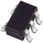
| 产品图片 |
|
| 产品型号 | ADT6501SRJZP065RL7 |
| rohs | 无铅 / 符合限制有害物质指令(RoHS)规范要求 |
| 产品系列 | - |
| 产品培训模块 | http://www.digikey.cn/PTM/IndividualPTM.page?site=cn&lang=zhs&ptm=21105 |
| 产品目录页面 | |
| 传感器类型 | 内部 |
| 供应商器件封装 | SOT-23-5 |
| 其它名称 | ADT6501SRJZP065RL7CT |
| 功能 | 温度开关 |
| 包装 | 剪切带 (CT) |
| 安装类型 | 表面贴装 |
| 封装/外壳 | SC-74A,SOT-753 |
| 工作温度 | -55°C ~ 125°C |
| 开关温度 | 65°C |
| 感应温度 | 65°C 跳变点 |
| 拓扑 | ADC, 比较器, 跳闸点寄存器 |
| 标准包装 | 1 |
| 特性 | - |
| 电压-电源 | 2.7 V ~ 5.5 V |
| 电流-电源 | 30µA |
| 电流-输出(最大值) | 20mA |
| 精度 | ±4°C |
| 视频文件 | http://www.digikey.cn/classic/video.aspx?PlayerID=1364138032001&width=640&height=505&videoID=2245193158001 |
| 输出 | 低有效 |
| 输出报警 | 是 |
| 输出类型 | 开路漏极 |
| 输出风扇 | 是 |


- 商务部:美国ITC正式对集成电路等产品启动337调查
- 曝三星4nm工艺存在良率问题 高通将骁龙8 Gen1或转产台积电
- 太阳诱电将投资9.5亿元在常州建新厂生产MLCC 预计2023年完工
- 英特尔发布欧洲新工厂建设计划 深化IDM 2.0 战略
- 台积电先进制程称霸业界 有大客户加持明年业绩稳了
- 达到5530亿美元!SIA预计今年全球半导体销售额将创下新高
- 英特尔拟将自动驾驶子公司Mobileye上市 估值或超500亿美元
- 三星加码芯片和SET,合并消费电子和移动部门,撤换高东真等 CEO
- 三星电子宣布重大人事变动 还合并消费电子和移动部门
- 海关总署:前11个月进口集成电路产品价值2.52万亿元 增长14.8%


PDF Datasheet 数据手册内容提取
Low Cost, 2.7 V to 5.5 V, Micropower Temperature Switches in SOT-23 Data Sheet ADT6501/ADT6502/ADT6503/ADT6504 FEATURES FUNCTIONAL BLOCK DIAGRAM ±0.5°C (typical) threshold accuracy VCC Factory-set trip points from 4 ADT6501 −45°C to +15°C in 10°C increments +35°C to +115°C in 10°C increments Σ-Δ No external components required TEMPERATURE-TO- DIGITAL CONVERTER COMPARATOR Maximum temperature of 125°C 5 TOVER Open-drain output (ADT6501/ADT6503) Push-pull output (ADT6502/ADT6504) Pin-selectable hysteresis of 2°C and 10°C FACTTROIPR YP OPRINETSET REGISTER Supply current of 30 µA (typical) Space-saving, 5-lead SOT-23 package 2ºC/10ºC AMPedPiLcaICl eAqTuIipOmNeSn t GN1D GN2D HY3ST 06096-001 Figure 1. Automotive Cell phones Hard disk drives Personal computers Electronic test equipment Domestic appliances Process control GENERAL DESCRIPTION The ADT6501/ADT6502/ADT6503/ADT6504 are trip point The ADT6503 and ADT6504 are used for monitoring tempera- temperature switches available in a 5-lead SOT-23 package. tures from −45°C to +15°C only. Therefore, the logic output Each part contains an internal band gap temperature sensor for pin becomes active when the temperature goes lower than the local temperature sensing. When the temperature crosses the selected trip point temperature. trip point setting, the logic output is activated. The ADT6501/ PRODUCT HIGHLIGHTS ADT6503 logic output is active low and open-drain. The 1. Σ-Δ based temperature measurement gives high accuracy ADT6502/ADT6504 logic output is active high and push-pull. and noise immunity. The temperature is digitized to a resolution of 0.125°C (11-bit). The factory trip point settings are 10°C apart starting from 2. Wide operating temperature range from −55°C to +125°C. −45°C to +15°C for the cold threshold models and from +35°C 3. ±0.5°C typical accuracy from −45°C to +115°C. to +115°C for the hot threshold models. 4. Factory threshold settings from −45°C to +115°C in These devices require no external components and typically 10°C increments. consume 30 μA supply current. Hysteresis is pin-selectable at 2°C and 10°C. The temperature switch is specified to operate 5. Supply voltage is 2.7 V to 5.5 V. over the supply range of 2.7 V to 5.5 V. 6. Supply current of 30 μA. The ADT6501 and ADT6502 are used for monitoring 7. Space-saving, 5-lead SOT-23 package. temperatures from +35°C to +115°C only. Therefore, the logic 8. Pin-selectable temperature hysteresis of 2°C or 10°C. output pin becomes active when the temperature goes higher 9. Temperature resolution of 0.125°C. than the selected trip point temperature. Rev. B Document Feedback Information furnished by Analog Devices is believed to be accurate and reliable. However, no responsibility is assumed by Analog Devices for its use, nor for any infringements of patents or other One Technology Way, P.O. Box 9106, Norwood, MA 02062-9106, U.S.A. rights of third parties that may result from its use. Specifications subject to change without notice. No license is granted by implication or otherwise under any patent or patent rights of Analog Devices. Tel: 781.329.4700 ©2007–2012 Analog Devices, Inc. All rights reserved. Trademarks and registered trademarks are the property of their respective owners. Technical Support www.analog.com
ADT6501/ADT6502/ADT6503/ADT6504 Data Sheet TABLE OF CONTENTS Features .............................................................................................. 1 Converter Details ..........................................................................8 Applications ....................................................................................... 1 Factory-Programmed Threshold Range ....................................8 Functional Block Diagram .............................................................. 1 Hysteresis Input .............................................................................8 General Description ......................................................................... 1 Temperature Conversion ..............................................................8 Product Highlights ........................................................................... 1 Application Information ................................................................ 10 Revision History ............................................................................... 2 Thermal Response Time ........................................................... 10 Specifications ..................................................................................... 3 Self-Heating Effects .................................................................... 10 Absolute Maximum Ratings ............................................................ 4 Supply Decoupling ..................................................................... 10 ESD Caution .................................................................................. 4 Temperature Monitoring ........................................................... 10 Pin Configurations and Function Descriptions ........................... 5 Typical Application Circuits ......................................................... 11 Typical Performance Characteristics ............................................. 6 Outline Dimensions ....................................................................... 13 Theory of Operation ........................................................................ 8 Ordering Guide .......................................................................... 13 Circuit Information ...................................................................... 8 REVISION HISTORY 9/12—Rev. A to Rev. B Changes to Product Highlights ....................................................... 1 Change to Supply Current Parameter, Table 1 .............................. 3 Changes to Table 1 ............................................................................. 3 Updated Outline Dimensions ....................................................... 13 Changes to Typical Performance Characteristics ......................... 6 Changes to Ordering Guide .......................................................... 13 1/08—Rev. 0 to Rev. A Added ADT6503 and ADT6504 ....................................... Universal 9/07—Revision 0: Initial Version Changes to Features .......................................................................... 1 Rev. B | Page 2 of 16
Data Sheet ADT6501/ADT6502/ADT6503/ADT6504 SPECIFICATIONS T = −55°C to +125°C, V = 2.7 V to 5.5 V, open-drain R = 10 kΩ, unless otherwise noted. A CC PULL-UP Table 1. Parameter Min Typ Max Unit Test Conditions/Comments TEMPERATURE SENSOR AND ADC Threshold Accuracy ±0.5 ±6 °C T = −45°C to −25°C A ±0.5 ±4 °C T = −15°C to +15°C A ±0.5 ±4 °C T = 35°C to 65°C A ±0.5 ±6 °C T = 75°C to 115°C A ADC Resolution 11 Bits Temperature Conversion Time 30 ms Time necessary to complete a conversion Update Rate 600 ms Conversion started every 600 ms Temperature Threshold Hysteresis 2 °C HYST pin = 0 V 10 °C HYST pin = V CC DIGITAL INPUT (HYST) Input Low Voltage, V 0.2 × V V IL CC Input High Voltage, V 0.8 × V V IH CC DIGITAL OUTPUT (OPEN-DRAIN) Output High Current, I 10 nA Leakage current, V = 2.7 V and V = 5.5 V OH CC OH Output Low Voltage, V 0.3 V I = 1.2 mA, V = 2.7 V OL OL CC 0.4 V I = 3.2 mA, V = 4.5 V OL CC Output Capacitance, C 1 10 pF R = 10 kΩ OUT PULL-UP DIGITAL OUTPUT (PUSH-PULL) Output Low Voltage, V 0.3 V I = 1.2 mA, V = 2.7 V OL OL CC 0.4 V I = 3.2 mA, V = 4.5 V OL CC Output High Voltage, V 0.8 × V V I = 500 µA, V = 2.7 V OH CC SOURCE CC V − 1.5 V I = 800 µA, V = 4.5 V CC SOURCE CC Output Capacitance, C 1 10 pF OUT POWER REQUIREMENTS Supply Voltage 2.7 5.5 V Supply Current 30 55 µA 1 Guaranteed by design and characterization. Rev. B | Page 3 of 16
ADT6501/ADT6502/ADT6503/ADT6504 Data Sheet ABSOLUTE MAXIMUM RATINGS Table 2. Stresses above those listed under Absolute Maximum Ratings Parameter Rating may cause permanent damage to the device. This is a stress V to GND −0.3 V to +7 V rating only; functional operation of the device at these or any CC HYST Input Voltage to GND −0.3 V to V + 0.3 V other conditions above those indicated in the operational CC Open-Drain Output Voltage to GND −0.3 V to +7 V section of this specification is not implied. Exposure to absolute Push-Pull Output Voltage to GND −0.3 V to V + 0.3 V maximum rating conditions for extended periods may affect CC Input Current on All Pins 20 mA device reliability. Output Current on All Pins 20 mA 0.9 Operating Temperature Range −55°C to +125°C 0.8 Storage Temperature Range −65°C to +160°C W) N ( 0.7 Maximum Junction Temperature, T 150.7°C O JMAX TI 5-Lead SOT-23 (RJ-5) PA 0.6 SI Power Dissipation1 WMAX = (TJMAX − TA2)/θJA R DIS 0.5 Thermal Impedance3 E W 0.4 θJA, Junction-to-Ambient (Still Air) 240°C/W M PO 0.3 IR Reflow Soldering U M (RoHS Compliant Package) XI 0.2 A M Peak Temperature 260°C (+0°C) 0.1 Time at Peak Temperature 20 sec to 40 sec SOT-23PD@125°C=0.107W 0 RRaammpp--DUpow Rnat Rea te −3°6C°/Cs/esce cm maxaixmimumum –55–50–40–30–20–100T1E0M2P0ER30AT4U0R5E0(6°0C)708090100110120125 06096-002 Time 25°C to Peak Temperature 8 minute maximum Figure 2. SOT-23 Maximum Power Dissipation vs. Temperature 1 Values relate to package being used on a standard 2-layer PCB. This gives a worst case θJA. Refer to Figure 2 for a plot of maximum power dissipation vs. ESD CAUTION ambient temperature (T). A 2 TA = ambient temperature. 3 Junction-to-case resistance is applicable to components featuring a preferential flow direction, for example, components mounted on a heat sink. Junction-to-ambient resistance is more useful for air-cooled, PCB-mounted components. Rev. B | Page 4 of 16
Data Sheet ADT6501/ADT6502/ADT6503/ADT6504 PIN CONFIGURATIONS AND FUNCTION DESCRIPTIONS ADT6501/ ADT6503/ ADT6502 ADT6504 GND 1 5 TOVER/ GND 1 5 TUNDER/ HGYNSDT 23 (NToOt Pto V SIEcWale) 4 TVOCCVER06096-003 HGYNSDT 23 (NToOt Pto V SIEcWale) 4 TVUCCNDER 06096-004 Figure 3. ADT6501/ADT6502 Pin Configuration Figure 4. ADT6503/ADT6504 Pin Configuration Table 3. Pin Function Descriptions Pin Number ADT6501 ADT6502 ADT6503 ADT6504 Mnemonic Description 1, 2 1, 2 1, 2 1, 2 GND Ground. 3 3 3 3 HYST Hysteresis Input. Connects HYST to GND for 2°C hysteresis or connects to V for 10°C hysteresis. CC 4 4 4 4 V Supply Input (2.7 V to 5.5 V). CC 5 — — — TOVER Open-Drain, Active Low Output. TOVER goes low when the temperature of the part exceeds the factory-programmed threshold; must use a pull-up resistor. — 5 — — TOVER Push-Pull, Active High Output. TOVER goes high when the temperature of the part exceeds the factory-programmed threshold. — — 5 — TUNDER Open-Drain, Active Low Output. TUNDER goes low when the temperature of the part exceeds the factory-programmed threshold; must use a pull-up resistor. — — — 5 TUNDER Push-Pull, Active High Output. TUNDER goes high when the temperature of the part exceeds the factory-programmed threshold. Rev. B | Page 5 of 16
ADT6501/ADT6502/ADT6503/ADT6504 Data Sheet TYPICAL PERFORMANCE CHARACTERISTICS 35 80 SAMPLE SIZE = 300 ED (%) 30 Ω) 70 RTS SAMPL 2250 SISTANCE ( 6500 2.7V 3.3V OF PA 15 NK RE 40 5.5V GE T SI 30 A U T 10 P EN UT 20 C O R PE 50 06096-015 100 06096-018 –0.5 –0.4 –0.3 –0.2 –0.1 0.1 0.2 0.3 0.4 0.5 –55 –10 25 70 100 125 TEMPERATURE ACCURACY (°C) TEMPERATURE (°C) Figure 5. Trip Threshold Accuracy Figure 8. Output Sink Resistance vs. Temperature 45 120 40 5V 100 35 3.3V 30 E (°C) 80 A) 25 UR I (µCC 20 PERAT 60 M 15 TE 40 10 20 50 06096-016 0 06096-019 –40 –10 25 75 120 0 1.6 3.2 4.8 6.4 8.0 9.6 11.2 12.8 0.8 2.4 4.0 5.6 7.2 8.8 10.4 12.0 TEMPERATURE (°C) TIME (s) Figure 6. Operating Supply Current vs. Temperature Figure 9. Thermal Step Response in Perfluorinated Fluid 180 140 160 Ω) 120 E ( 140 NC 2.7V 100 RESISTA 112000 3.3V URE (°C) 80 E 5.5V AT URC 80 PER 60 O M UT S 60 TE 40 P T 40 U O 200 06096-017 200 06096-020 –55 –10 25 70 100 125 3.6 10.8 18.0 25.2 32.4 39.6 46.8 54.0 61.2 0 7.2 14.4 21.6 28.8 36.0 43.2 50.4 57.6 TEMPERATURE (°C) TIME (s) Figure 7. ADT6502/ADT6504 Output Source Resistance vs. Temperature Figure 10. Thermal Step Response in Still Air Rev. B | Page 6 of 16
Data Sheet ADT6501/ADT6502/ADT6503/ADT6504 12 10 10°C C) 8 VCC S (° VCC = 3.3V 1 SI RE 6 E T S Y H 4 TOVER 2°C 2 2 0 –45 –25 –15 15 25 35 65 75 115 06096-021 CH1 2.0V CH2 2.0V M 10.0ms 50.0kS/s 20.0µs/pt 06096-023 TEMPERATURE (°C) A CH1 1.68V Figure 11. Hysteresis vs. Trip Temperature Figure 13. ADT6501 Start-Up Delay 45 40 35 VCC 30 1 A) 25 µ (C C 20 I 15 TOVER 2 10 –40ºC –10ºC +25ºC 06096-022 50 ++7152º0CºC 06096-024 CH1 2.0V CH2 2.0V M 10.0µs 50.0MS/s 20.0ns/pt 2.42.62.83.03.23.43.63.84.04.24.44.64.85.05.25.45.6 A CH1 1.68V VCC (V) Figure 12. ADT6501 Start-Up and Power-Down Figure 14. Operating Supply Current vs. Voltage Over Temperature Rev. B | Page 7 of 16
ADT6501/ADT6502/ADT6503/ADT6504 Data Sheet THEORY OF OPERATION CIRCUIT INFORMATION FACTORY-PROGRAMMED THRESHOLD RANGE The ADT6501/ADT6502/ADT6503/ADT6504 are 11-bit digital The ADT6501/ADT6502/ADT6503/ADT6504 are available temperature sensors with a 12th bit acting as the sign bit. An with factory-set threshold levels ranging from −45°C to +115°C on-board temperature sensor generates a voltage precisely in 10°C temperature steps. The ADT6501/ADT6503 outputs are proportional to absolute temperature, which is compared to intended to interface to reset inputs of microprocessors. The an internal voltage reference and input to a precision digital ADT6502/ADT6504 are intended for driving circuits of modulator. The 12-bit output from the modulator is input into a applications such as fan control circuits. Table 4 lists the digital comparator where it is compared with a factory-set trip available temperature threshold ranges. level. The output trip pin is activated if the temperature measured Table 4. Factory-Set Temperature Threshold Ranges is greater than, in the case of the ADT6501/ADT6502, or less Device Threshold (T ) Range than, in the case of the ADT6503/ADT6504, the factory-set trip TH ADT6501 +35°C < T < +115°C level. Overall accuracy for the ADT650x family is ±6°C TH ADT6502 +35°C < T < +115°C (maximum) from −45°C to +115°C. TH ADT6503 −45°C < T < +15°C The on-board temperature sensor has excellent accuracy and TH ADT6504 −45°C < T < +15°C linearity over the entire rated temperature range without needing TH correction or calibration by the user. The ADT6501/ADT6503 HYSTERESIS INPUT have active low, open-drain output structures that can sink The HYST pin is used to select a temperature hysteresis of 2°C or current. The ADT6502/ADT6504 have active high, push-pull 10°C. The digital comparator ensures excellent accuracy for the output structures that can sink and source current. On power- hysteresis value. If the HYST pin is connected to V , a hysteresis up, the output becomes active when the first conversion is CC of 10°C is selected. If the HYST pin is connected to GND, a completed, which typically takes 30 ms. hysteresis of 2°C is selected. The HYST pin should not be left The sensor output is digitized by a first-order, ∑-∆ modulator, floating. Hysteresis prevents oscillation on the output pin when also known as the charge balance type analog-to-digital the temperature is approaching the trip point and after the converter (ADC). This type of converter utilizes time domain output pin is activated. For example, if the temperature trip is oversampling and a high accuracy comparator to deliver 11 bits 45°C and the hysteresis selected is 10°C, the temperature would of effective accuracy in an extremely compact circuit. have to go as low as 35°C before the output deactivates. CONVERTER DETAILS TEMPERATURE CONVERSION The Σ-Δ modulator consists of an input sampler, a summing The conversion clock for the part is generated internally. No network, an integrator, a comparator, and a 1-bit digital-to- external clock is required. The internal clock oscillator runs an analog converter (DAC). Similar to the voltage-to-frequency automatic conversion sequence. During this automatic conversion converter, this architecture creates a negative feedback loop and sequence, a conversion is initiated every 600 ms. At this time, the minimizes the integrator output by changing the duty cycle of part powers up its analog circuitry and performs a temperature the comparator output in response to input voltage changes. conversion. The comparator samples the output of the integrator at a much This temperature conversion typically takes 30 ms, after which higher rate than the input sampling frequency; this is called the analog circuitry of the part automatically shuts down. The oversampling. Oversampling spreads the quantization noise analog circuitry powers up again 570 ms later, when the 600 ms over a much wider band than that of the input signal, timer times out and the next conversion begins. The result of improving overall noise performance and increasing accuracy. the most recent temperature conversion is compared with the factory-set trip point value. If the temperature measured is greater than the trip point value, the output is activated. The output is deactivated once the temperature crosses back over the trip point threshold plus whatever temperature hysteresis is selected. Figure 15 to Figure 18 show the transfer function for the output trip pin of each generic model. Rev. B | Page 8 of 16
Data Sheet ADT6501/ADT6502/ADT6503/ADT6504 V V TUNDER TOVER COLD HOT COLD HOT 10°C HYST TTH TEMP TTH TEMP H2Y°SCT 06096-006 H2Y°SCT H1Y0°SCT 06096-008 Figure 15. ADT6501 TOVER Transfer Function Figure 17. ADT6503 TUNDER Transfer Function V V TOVER TUNDER COLD HOT COLD HOT TTH TEMP TTH TEMP H1Y0°SCT H2Y°SCT 06096-007 H2Y°SCT H1Y0°SCT 06096-009 Figure 16. ADT6502 TOVER Transfer Function Figure 18. ADT6504 TUNDER Transfer Function Rev. B | Page 9 of 16
ADT6501/ADT6502/ADT6503/ADT6504 Data Sheet APPLICATION INFORMATION THERMAL RESPONSE TIME If possible, the ADT650x should be powered directly from the system power supply. This arrangement, shown in Figure 19, The time required for a temperature sensor to settle to a specified isolates the analog section from the logic switching transients. accuracy is a function of the sensor’s thermal mass and the Even if a separate power supply trace is not available, generous thermal conductivity between the sensor and the object being supply bypassing reduces supply line induced errors. Local sensed. Thermal mass is often considered equivalent to supply bypassing consisting of a 0.1 µF ceramic capacitor is capacitance. Thermal conductivity is commonly specified using advisable to achieve the temperature accuracy specifications. the symbol Q and can be thought of as thermal resistance. It is This decoupling capacitor must be placed as close as possible to commonly specified in units of degrees per watt of power the ADT650x V pin. transferred across the thermal joint. Thus, the time required for CC the ADT650x to settle to the desired accuracy is dependent on TTL/CMOS LOGIC the characteristics of the SOT-23 package, the thermal contact CIRCUITS 0.1µF ADT650x established in that particular application, and the equivalent power of the heat source. In most applications, the settling time is best determined empirically. SThEeL tFe-mHpEeAraTtuIrNe Gm eEaFsuFrEeCmTenSt accuracy of the ADT6501/ SPUOPWPELRY 06096-010 Figure 19. Separate Traces Used to Reduce Power Supply Noise ADT6502/ADT6503/ADT6504 can be degraded in some TEMPERATURE MONITORING applications due to self-heating. Errors can be introduced from the quiescent dissipation and power dissipated when converting. The ADT6501/ADT6502/ADT6503/ADT6504 are ideal for The magnitude of these temperature errors depends on the monitoring the thermal environment within electronic equipment. thermal conductivity of the ADT650x package, the mounting For example, the surface-mount package accurately reflects the technique, and the effects of airflow. At 25°C, static dissipation exact thermal conditions that affect nearby integrated circuits. in the ADT650x is typically 99 µW operating at 3.3 V. In the The ADT650x measure and convert the temperature at the 5-lead SOT-23 package mounted in free air, this accounts for a surface of its own semiconductor chip. When the ADT650x are temperature increase due to self-heating of used to measure the temperature of a nearby heat source, the ΔT = PDISS × θJA = 99 µW × 240°C/W = 0.024°C thermal impedance between the heat source and the ADT650x It is recommended that current dissipated through the device be must be as low as possible. kept to a minimum because it has a proportional effect on the As much as 60% of the heat transferred from the heat source to temperature error. the thermal sensor on the ADT650x die is discharged via the SUPPLY DECOUPLING copper tracks, package pins, and bond pads. Of the pins on the ADT650x, the GND pins transfer most of the heat. Therefore, The ADT6501/ADT6502/ADT6503/ADT6504 should be to monitor the temperature of a heat source, it is recommended decoupled with a 0.1 µF ceramic capacitor between V and CC that the thermal resistance between the ADT650x GND pins GND. This is particularly important when the ADT650x are and the GND of the heat source be reduced as much as possible. mounted remotely from the power supply. Precision analog products such as the ADT650x require well filtered power For example, the unique properties of the ADT650x can be used sources. Because the ADT650x operate from a single supply, it to monitor a high power dissipation microprocessor. The may seem convenient to tap into the digital logic power supply. ADT650x device in its SOT-23 package is mounted directly beneath the microprocessor’s pin grid array (PGA) package. Unfortunately, the logic supply is often a switch-mode design, The ADT650x requires no external characterization. which generates noise in the 20 kHz to 1 MHz range. In addition, fast logic gates can generate glitches that are hundreds of mV in amplitude due to wiring resistance and inductance. Rev. B | Page 10 of 16
Data Sheet ADT6501/ADT6502/ADT6503/ADT6504 TYPICAL APPLICATION CIRCUITS 3.3V 3.3V 12V 0.1µF 0.1µF 100kΩ VCC VCC VCC ADT6501 ADT6502 MICROPROCESSOR TOVER INT HYST TOVER GND HYST GND GND GND GND 06096-011 06096-012 Figure 20. Microprocessor Alarm Figure 21. Overtemperature Fan Control 3.3V 0.1µF VCC ADT6502 ... P075 TOVER OVER TEMPERATURE GND HYST GND OUT OF RANGE 0.1µF VCC ADT6504 ... N015 TUNDER UNDER TEMPERATURE GND HYST GND 06096-013 Figure 22. Temperature Window Alarms Rev. B | Page 11 of 16
ADT6501/ADT6502/ADT6503/ADT6504 Data Sheet 3.3V 0.1µF 100kΩ VCC VCC ADT6501 MICROPROCESSOR ... P075 TOVER INT GND HYST GND GND 12V 0.1µF VCC ADT6502 ... P045 TOVER GND HYST GND 06096-014 Figure 23. Fail-Safe Temperature Monitor Rev. B | Page 12 of 16
Data Sheet ADT6501/ADT6502/ADT6503/ADT6504 OUTLINE DIMENSIONS 3.00 2.90 2.80 1.70 5 4 3.00 1.60 2.80 1.50 2.60 1 2 3 0.95BSC 1.90 BSC 1.30 1.15 0.90 1.45MAX 0.20MAX 0.95MIN 0.08MIN 0.55 0.15MAX 10° 0.45 0.05MIN 0.50MAX SPELAATNIENG 5° B0S.6C0 0.35 0.35MIN 0° COMPLIANTTOJEDECSTANDARDSMO-178-AA 11-01-2010-A Figure 24. 5-Lead Small Outline Transistor Package [SOT-23] (RJ-5) Dimensions shown in millimeters ORDERING GUIDE Accuracy @ Threshold Threshold Temperature Package Package Ordering Model1 Temperature Temperature Range Description Option Quantity Branding ADT6501SRJZP035RL7 35°C ±4°C −55°C to +125°C 5-Lead SOT-23 RJ-5 3,000 T1U ADT6501SRJZP045RL7 45°C ±4°C −55°C to +125°C 5-Lead SOT-23 RJ-5 3,000 T1V ADT6501SRJZP055RL7 55°C ±4°C −55°C to +125°C 5-Lead SOT-23 RJ-5 3,000 T0B ADT6501SRJZP065RL7 65°C ±4°C −55°C to +125°C 5-Lead SOT-23 RJ-5 3,000 T1W ADT6501SRJZP075RL7 75°C ±6°C −55°C to +125°C 5-Lead SOT-23 RJ-5 3,000 T1X ADT6501SRJZP085RL7 85°C ±6°C −55°C to +125°C 5-Lead SOT-23 RJ-5 3,000 T0W ADT6501SRJZP085-RL 85°C ±6°C −55°C to +125°C 5-Lead SOT-23 RJ-5 10,000 T0W ADT6501SRJZP095RL7 95°C ±6°C −55°C to +125°C 5-Lead SOT-23 RJ-5 3,000 T1Y ADT6501SRJZP105RL7 105°C ±6°C −55°C to +125°C 5-Lead SOT-23 RJ-5 3,000 T15 ADT6501SRJZP105-RL 105°C ±6°C −55°C to +125°C 5-Lead SOT-23 RJ-5 10,000 T15 ADT6501SRJZP115RL7 115°C ±6°C −55°C to +125°C 5-Lead SOT-23 RJ-5 3,000 T1Z ADT6502SRJZP035RL7 35°C ±4°C −55°C to +125°C 5-Lead SOT-23 RJ-5 3,000 T25 ADT6502SRJZP045RL7 45°C ±4°C −55°C to +125°C 5-Lead SOT-23 RJ-5 3,000 T26 ADT6502SRJZP055RL7 55°C ±4°C −55°C to +125°C 5-Lead SOT-23 RJ-5 3,000 T27 ADT6502SRJZP065RL7 65°C ±4°C −55°C to +125°C 5-Lead SOT-23 RJ-5 3,000 T28 ADT6502SRJZP075RL7 75°C ±6°C −55°C to +125°C 5-Lead SOT-23 RJ-5 3,000 T17 ADT6502SRJZP085RL7 85°C ±6°C −55°C to +125°C 5-Lead SOT-23 RJ-5 3,000 T29 ADT6502SRJZP095RL7 95°C ±6°C −55°C to +125°C 5-Lead SOT-23 RJ-5 3,000 T2B ADT6502SRJZP105RL7 105°C ±6°C −55°C to +125°C 5-Lead SOT-23 RJ-5 3,000 T2C ADT6502SRJZP115RL7 115°C ±6°C −55°C to +125°C 5-Lead SOT-23 RJ-5 3,000 T2D ADT6503SRJZN045RL7 −45°C ±6°C −55°C to +125°C 5-Lead SOT-23 RJ-5 3,000 T2E ADT6503SRJZN035RL7 −35°C ±6°C −55°C to +125°C 5-Lead SOT-23 RJ-5 3,000 T2F ADT6503SRJZN025RL7 −25°C ±6°C −55°C to +125°C 5-Lead SOT-23 RJ-5 3,000 T19 ADT6503SRJZN015RL7 −15°C ±4°C −55°C to +125°C 5-Lead SOT-23 RJ-5 3,000 T2J ADT6503SRJZN005RL7 −5°C ±4°C −55°C to +125°C 5-Lead SOT-23 RJ-5 3,000 T2M Rev. B | Page 13 of 16
ADT6501/ADT6502/ADT6503/ADT6504 Data Sheet Accuracy @ Threshold Threshold Temperature Package Package Ordering Model1 Temperature Temperature Range Description Option Quantity Branding ADT6503SRJZP005RL7 +5°C ±4°C −55°C to +125°C 5-Lead SOT-23 RJ-5 3,000 T2N ADT6503SRJZP015RL7 +15°C ±4°C −55°C to +125°C 5-Lead SOT-23 RJ-5 3,000 T2P ADT6504SRJZN045RL7 −45°C ±6°C −55°C to +125°C 5-Lead SOT-23 RJ-5 3,000 T2K ADT6504SRJZN035RL7 −35°C ±6°C −55°C to +125°C 5-Lead SOT-23 RJ-5 3,000 T2L ADT6504SRJZN025RL7 −25°C ±6°C −55°C to +125°C 5-Lead SOT-23 RJ-5 3,000 T2Q ADT6504SRJZN015RL7 −15°C ±4°C −55°C to +125°C 5-Lead SOT-23 RJ-5 3,000 T2R ADT6504SRJZN005RL7 −5°C ±4°C −55°C to +125°C 5-Lead SOT-23 RJ-5 3,000 T2T ADT6504SRJZP005RL7 +5°C ±4°C −55°C to +125°C 5-Lead SOT-23 RJ-5 3,000 T2H ADT6504SRJZP015RL7 +15°C ±4°C −55°C to +125°C 5-Lead SOT-23 RJ-5 3,000 T2U 1 Z = RoHS Compliant Part. Rev. B | Page 14 of 16
Data Sheet ADT6501/ADT6502/ADT6503/ADT6504 NOTES Rev. B | Page 15 of 16
ADT6501/ADT6502/ADT6503/ADT6504 Data Sheet NOTES ©2007–2012 Analog Devices, Inc. All rights reserved. Trademarks and registered trademarks are the property of their respective owners. D06096-0-10/12(B) Rev. B | Page 16 of 16