ICGOO在线商城 > 集成电路(IC) > 数据采集 - 模数转换器 > ADS1213U
 Datasheet下载
- 型号: ADS1213U
- 制造商: Texas Instruments
- 库位|库存: xxxx|xxxx
- 要求:
| 数量阶梯 | 香港交货 | 国内含税 |
| +xxxx | $xxxx | ¥xxxx |
查看当月历史价格
查看今年历史价格
ADS1213U产品简介:
ICGOO电子元器件商城为您提供ADS1213U由Texas Instruments设计生产,在icgoo商城现货销售,并且可以通过原厂、代理商等渠道进行代购。 ADS1213U价格参考¥107.79-¥179.77。Texas InstrumentsADS1213U封装/规格:数据采集 - 模数转换器, 22 Bit Analog to Digital Converter 4 Input 1 Sigma-Delta 24-SOIC。您可以下载ADS1213U参考资料、Datasheet数据手册功能说明书,资料中有ADS1213U 详细功能的应用电路图电压和使用方法及教程。
Texas Instruments(德州仪器)的ADS1213U是一款高精度、低功耗的24位模数转换器(ADC),属于数据采集系统中的核心组件。其应用场景主要包括以下领域:

1. 工业自动化与控制
   ADS1213U适用于工业设备中的精密测量,例如压力传感器、温度传感器和流量计的数据采集。其高分辨率和低噪声特性使其能够准确捕捉微小信号变化,为控制系统提供可靠输入。

2. 医疗设备
   在医疗领域,该芯片可用于心电图(ECG)、血压监测仪和血糖仪等设备中。其高精度性能确保了对生物电信号的精确测量,同时低功耗设计延长了便携式医疗设备的电池寿命。

3. 环境监测
   ADS1213U可应用于环境监测系统,如空气质量检测、水质分析和气象站。它能高效处理来自传感器的模拟信号,转化为数字数据以便进一步分析和记录。

4. 称重系统与衡器
   该芯片适合用于电子秤和其他需要高精度重量测量的场合。其内置的可编程增益放大器(PGA)可以放大微弱信号,从而提高测量精度。

5. 农业与物联网(IoT)
   在智慧农业中,ADS1213U可用于土壤湿度、pH值和养分水平的监测。结合物联网技术,这些数据可以帮助农民优化资源利用和作物管理。

6. 汽车电子
   ADS1213U也可用于汽车传感器数据采集,如胎压监测系统(TPMS)或悬架系统的状态监控,以提升车辆的安全性和舒适性。

总之,ADS1213U凭借其卓越的性能和灵活性,广泛适用于需要高精度数据采集的各种场景,尤其在对功耗敏感的应用中表现出色。
| 参数 | 数值 |
| 产品目录 | 集成电路 (IC)半导体 |
| 描述 | IC 22-BIT DELTA-SIGMA A/D 24SOIC模数转换器 - ADC 22-Bit Anlg-to-Dig Converter |
| 产品分类 | |
| 品牌 | Texas Instruments |
| 产品手册 | |
| 产品图片 |
|
| rohs | 符合RoHS无铅 / 符合限制有害物质指令(RoHS)规范要求 |
| 产品系列 | 数据转换器IC,模数转换器 - ADC,Texas Instruments ADS1213U- |
| 数据手册 | |
| 产品型号 | ADS1213U |
| 产品培训模块 | http://www.digikey.cn/PTM/IndividualPTM.page?site=cn&lang=zhs&ptm=13240 |
| 产品目录页面 | |
| 产品种类 | 模数转换器 - ADC |
| 位数 | 22 |
| 供应商器件封装 | 24-SOIC |
| 信噪比 | Yes |
| 分辨率 | 22 bit |
| 制造商产品页 | http://www.ti.com/general/docs/suppproductinfo.tsp?distId=10&orderablePartNumber=ADS1213U |
| 包装 | 管件 |
| 单位重量 | 624.400 mg |
| 商标 | Texas Instruments |
| 安装类型 | 表面贴装 |
| 安装风格 | SMD/SMT |
| 封装 | Tube |
| 封装/外壳 | 24-SOIC(0.295",7.50mm 宽) |
| 封装/箱体 | SOIC-24 |
| 工作温度 | -40°C ~ 85°C |
| 工作电源电压 | 4.75 V to 5.25 V |
| 工厂包装数量 | 25 |
| 接口类型 | SSI |
| 数据接口 | SPI |
| 最大功率耗散 | 8.5 mW |
| 最大工作温度 | + 85 C |
| 最小工作温度 | - 40 C |
| 标准包装 | 25 |
| 电压参考 | 2.5 V |
| 电压源 | 模拟和数字 |
| 系列 | ADS1213 |
| 结构 | Sigma-Delta |
| 视频文件 | http://www.digikey.cn/classic/video.aspx?PlayerID=1364138032001&width=640&height=455&videoID=44659313001 |
| 转换器数 | 1 |
| 转换器数量 | 1 |
| 转换速率 | 6.25 kS/s |
| 输入数和类型 | 8 个单端,单极8 个单端,双极4 个差分,单极4 个差分,双极 |
| 输入类型 | Differential |
| 通道数量 | 4 Channel |
| 采样率(每秒) | 6.25k |


- 商务部:美国ITC正式对集成电路等产品启动337调查
- 曝三星4nm工艺存在良率问题 高通将骁龙8 Gen1或转产台积电
- 太阳诱电将投资9.5亿元在常州建新厂生产MLCC 预计2023年完工
- 英特尔发布欧洲新工厂建设计划 深化IDM 2.0 战略
- 台积电先进制程称霸业界 有大客户加持明年业绩稳了
- 达到5530亿美元!SIA预计今年全球半导体销售额将创下新高
- 英特尔拟将自动驾驶子公司Mobileye上市 估值或超500亿美元
- 三星加码芯片和SET,合并消费电子和移动部门,撤换高东真等 CEO
- 三星电子宣布重大人事变动 还合并消费电子和移动部门
- 海关总署:前11个月进口集成电路产品价值2.52万亿元 增长14.8%


PDF Datasheet 数据手册内容提取
ADS1212 ADS1212 ADS1213 ADS1213 ADS1212 ADS1213 ADS1213 SBAS064B – JANUARY 1996 – REVISED FEBRUARY 2004 22-Bit ANALOG-TO-DIGITAL CONVERTER FEATURES DESCRIPTION (cid:1) DELTA-SIGMA A/D CONVERTER The ADS1212 and ADS1213 are precision, wide dynamic (cid:1) 22 BITS NO MISSING CODES range, delta-sigma Analog-to-Digital (A/D) converters with (cid:1) 20 BITS EFFECTIVE RESOLUTION AT 10Hz 24-bit resolution operating from a single +5V supply. The differential inputs are ideal for direct connection to transduc- AND 16 BITS AT 1000Hz ers or low-level voltage signals. The delta-sigma architec- (cid:1) LOW POWER: 1.4mW ture is used for wide dynamic range and to ensure 22 bits of (cid:1) DIFFERENTIAL INPUTS no-missing-code performance. An effective resolution of 20 (cid:1) PROGRAMMABLE GAIN AMPLIFIER bits is achieved through the use of a very low-noise input (cid:1) SPI™ COMPATIBLE SSI INTERFACE amplifier at conversion rates up to 10Hz. Effective resolu- tions of 16 bits can be maintained up to a sample rate of (cid:1) PROGRAMMABLE CUTOFF FREQUENCY 1kHz through the use of the unique Turbo Modulator mode UP TO 6.25kHz of operation. The dynamic range of the converters is further (cid:1) INTERNAL/EXTERNAL REFERENCE increased by providing a low-noise programmable gain (cid:1) ON-CHIP SELF-CALIBRATION amplifier with a gain range of 1 to 16 in binary steps. (cid:1) ADS1213 INCLUDES 4-CHANNEL MUX The ADS1212 and ADS1213 are designed for high-resolution measurement applications in smart transmitters, industrial APPLICATIONS process control, weigh scales, chromatography and portable instrumentation. Both converters include a flexible synchro- (cid:1) INDUSTRIAL PROCESS CONTROL nous serial interface that is SPI compatible and also offers a (cid:1) INSTRUMENTATION two-wire control mode for low-cost isolation. (cid:1) BLOOD ANALYSIS The ADS1212 is a single channel converter and is offered in (cid:1) SMART TRANSMITTERS both DIP-18 and SO-18 packages. The ADS1213 includes a 4-channel input multiplexer and is available in DIP-24, (cid:1) PORTABLE INSTRUMENTS SO-24, and SSOP-28 packages. (cid:1) WEIGH SCALES (cid:1) PRESSURE TRANSDUCERS AGND AVDD REFOUT REFIN VBIAS XIN XOUT +2.5V +3.3V Bias AIN1P Reference Generator Clock Generator DGND AIN1N DVDD AIN2P Micro Controller AAIINN23NP MUX AAIINNNP PGA SeMcoond∆du∑-laOtordrer DThigiritda-lO Fridlteerr DICnaostamtr uOmcuatitnopdnu tRR Reeegggiissistteeterrr AIN3N Offset Register Full-Scale Register AIN4P AIN4N SCLK Modulator Control Serial Interface SDIO SDOUT ADS1213 Only ADS1212, 1213 DSYNC CS MODE DRDY PATENTS PENDING Please be aware that an important notice concerning availability, standard warranty, and use in critical applications of Texas Instruments semiconductor products and disclaimers thereto appears at the end of this data sheet. All trademarks are the property of their respective owners. PRODUCTION DATA information is current as of publication date. Copyright © 1996-2004, Texas Instruments Incorporated Products conform to specifications per the terms of Texas Instruments standard warranty. Production processing does not necessarily include testing of all parameters. www.ti.com
SPECIFICATIONS All specifications T to T , AV = DV = +5V, f = 1MHz, programmable gain amplifier setting of 1, Turbo Mode Rate of 1, REF disabled, V disabled, MIN MAX DD DD XIN OUT BIAS and external 2.5V reference, unless otherwise specified. ADS1212U, P/ADS1213U, P, E PARAMETER CONDITIONS MIN TYP MAX UNITS ANALOG INPUT Input Voltage Range(1) 0 +5 V With V (2) –10 +10 V BIAS Input Impedance G = Gain, TMR = Turbo Mode Rate 20/(G • TMR)(3) MΩ Programmable Gain Amplifier User Programmable: 1, 2, 4, 8, or 16 1 16 Input Capacitance 5 pF Input Leakage Current At +25°C 5 50 pA T to T 1 nA MIN MAX SYSTEMS PERFORMANCE No Missing Codes f = 10Hz 22 Bits DATA f = 60Hz 19 Bits DATA f = 100Hz, TMR of 4 21 Bits DATA f = 250Hz, TMR of 8 20 Bits DATA f = 500Hz, TMR of 16 20 Bits DATA f = 1000Hz, TMR of 16 18 Bits DATA Integral Linearity f = 60Hz ±0.0015 %FSR DATA f = 1000Hz, TMR of 16 ±0.0015 %FSR DATA Integral Linearity (Single-Ended) 0.01 %FSR Unipolar Offset Error(4) See Note 5 Unipolar Offset Drift(6) 1 ppm/°C Gain Error(4) See Note 5 Gain Error Drift(6) 4 ppm/°C Common-Mode Rejection(9) At DC, T to T 90 100 dB MIN MAX 50Hz, f = 50Hz(7) 160 dB DATA 60Hz, f = 60Hz(7) 160 dB DATA Normal-Mode Rejection 50Hz, f = 50Hz(7) 100 dB DATA 60Hz, f = 60Hz(7) 100 dB DATA Output Noise See Typical Performance Curves Power Supply Rejection DC, 50Hz, and 60Hz 60 dB VOLTAGE REFERENCE Internal Reference (REF ) 2.4 2.5 2.6 V OUT Drift 25 ppm/°C Noise 50 µVp-p Load Current Source or Sink 1 mA Output Impedance 2 Ω External Reference (REF ) 2.0 3.0 V IN Load Current 2.5 µA V Output Using Internal Reference 3.15 3.3 3.45 V BIAS Drift 50 ppm/°C Load Current Source or Sink 10mA DIGITAL INPUT/OUTPUT Logic Family TTL Compatible CMOS Logic Level: (all except X ) IN V I = +5µA 2.0 DV +0.3 V IH IH DD V I = +5µA –0.3 0.8 V IL IL V I = 2 TTL Loads 2.4 V OH OH V I = 2 TTL Loads 0.4 V OL OL X Input Levels: V 3.5 DV +0.3 V IN IH DD V –0.3 0.8 V IL X Frequency Range (f ) 0.5 2.5 MHz IN XIN Output Data Rate (f ) User Programmable and TMR = 1 to 16 0.96 6,250 Hz DATA f = 500kHz 0.48 3,125 Hz XIN f = 2.5MHz 2.4 15,625 Hz XIN Data Format User Programmable Two’s Complement or Offset Binary SYSTEM CALIBRATION Offset and Full-Scale Limits V = Full-Scale Differential Voltage(8) 0.7 • (2 • REF )/G FS IN V – | V | V = Offset Differential Voltage(8) 1.3 • (2 • REF )/G FS OS OS IN ADS1212, 1213 2 SBAS064A
SPECIFICATIONS (Cont.) All specifications T to T , AV = DV = +5V, f = 1MHz, programmable gain amplifier setting of 1, Turbo Mode Rate of 1, REF disabled, V disabled, MIN MAX DD DD XIN OUT BIAS and external 2.5V reference, unless otherwise specified. ADS1212U, P/ADS1213U, P, E PARAMETER CONDITIONS MIN TYP MAX UNITS POWER SUPPLY REQUIREMENTS Power Supply Voltage 4.75 5.25 V Power Supply Current: Analog Current 95 µA Digital Current 185 µA Additional Analog Current with REF Enabled 1.8 mA OUT V Enabled No Load 1 mA BIAS Power Dissipation At +25°C 1.4 mW T to T 1.8 mW MIN MAX TMR of 16 6 8.5 mW f = 2.5MHz 2.2 mW XIN f = 2.5MHz, TMR of 16 7.5 mW XIN Sleep Mode 0.45 mW TEMPERATURE RANGE Specified –40 +85 °C Storage –60 +125 °C NOTES: (1) In order to achieve the converter’s full-scale range, the input must be fully differential (A N = 2 • REF – A P). If the input is single-ended (A N or IN IN IN IN A P is fixed), then the full-scale range is one-half that of the differential range. (2) This range is set with external resistors and V (as described in the text). IN BIAS Other ranges are possible. (3) Input impedance is higher with lower f . (4) Applies after calibration. (5) After system calibration, these errors will be of the order XIN of the effective resolution of the converter. Refer to the Typical Performance Curves which apply to the desired mode of operation. (6) Recalibration can remove these errors. (7) The specification also applies at f /i, where i is 2, 3, 4, etc. (8) Voltages at the analog inputs must remain within AGND to AV . (9) The common- DATA DD mode rejection test is performed with 100mV differential input. ABSOLUTE MAXIMUM RATINGS ELECTROSTATIC Analog Input: Current................................................±100mA, Momentary DISCHARGE SENSITIVITY ±10mA, Continuous Voltage...................................AGND –0.3V to AV +0.3V DD This integrated circuit can be damaged by ESD. Texas AV to DV ...........................................................................–0.3V to 6V DD DD AV to AGND.........................................................................–0.3V to 6V Instruments recommends that all integrated circuits be handled DD DVDD to DGND.........................................................................–0.3V to 6V with appropriate precautions. Failure to observe proper han- AGND to DGND................................................................................±0.3V dling and installation procedures can cause damage. REF Voltage to AGND............................................–0.3V to AV +0.3V IN DD Digital Input Voltage to DGND..................................–0.3V to DVDD +0.3V ESD damage can range from subtle performance degrada- Digital Output Voltage to DGND...............................–0.3V to DV +0.3V Lead Temperature (soldering, 10s) ..............................................D D+300°C tion to complete device failure. Precision integrated circuits Power Dissipation (Any package)..................................................500mW may be more susceptible to damage because very small parametric changes could cause the device not to meet its published specifications. PACKAGE/ORDERING INFORMATION For the latest package and ordering information, see the Package Option Addendum located at the end of this data sheet. ADS1212, 1213 3 SBAS064A
ADS1212 SIMPLIFIED BLOCK DIAGRAM AGND AV REF REF V X X DD OUT IN BIAS IN OUT 3 16 17 18 4 7 8 +2.5V +3.3V Bias Clock Generator 9 DGND Reference Generator 10 DV DD Micro Controller 1 AINP Second-Order Instruction Register ∆Σ Third-Order PGA Command Register A N 2 Modulator Digital Filter Data Output Register IN Offset Register Full-Scale Register 11 SCLK Modulator Control Serial Interface 12 SDIO 13 SDOUT 6 5 15 14 DSYNC CS MODE DRDY ADS1212 PIN CONFIGURATION ADS1212 PIN DEFINITIONS TOP VIEW DIP/SOIC PIN NO NAME DESCRIPTION 1 A P Noninverting Input. IN 2 A N Inverting Input. IN 3 AGND Analog Ground. AINP 1 18 REFIN 4 VBIAS Bias Voltage Output, +3.3V nominal. 5 CS Chip Select Input. A N 2 17 REF IN OUT 6 DSYNC Control Input to Synchronize Serial Output Data. AGND 3 16 AV 7 X System Clock Input. DD IN 8 X System Clock Output. V 4 15 MODE OUT BIAS 9 DGND Digital Ground. ADS1212 CS 5 14 DRDY 10 DV Digital Supply, +5V nominal. DD 11 SCLK Clock Input/Output for serial data transfer. DSYNC 6 13 SDOUT 12 SDIO Serial Data Input (can also function as Serial Data X 7 12 SDIO Output). IN 13 SDOUT Serial Data Output. X 8 11 SCLK OUT 14 DRDY Data Ready. DGND 9 10 DV 15 MODE SCLK Control Input (Master = 1, Slave = 0). DD 16 AV Analog Supply, +5V nominal. DD 17 REF Reference Output, +2.5V nominal. OUT 18 REF Reference Input. IN ADS1212, 1213 4 SBAS064A
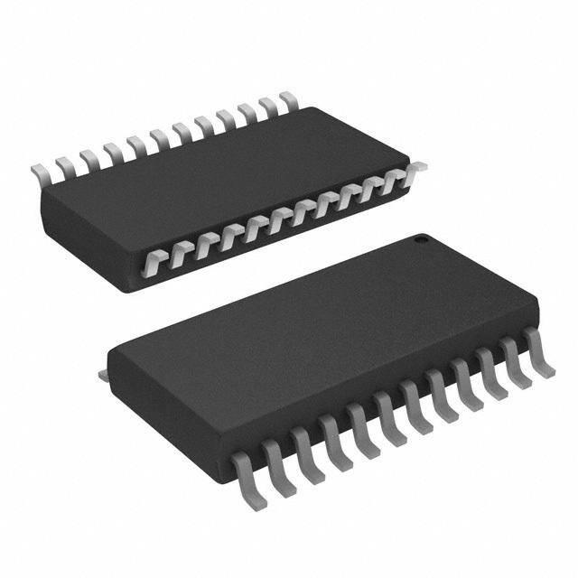
ADS1213 SIMPLIFIED BLOCK DIAGRAM AGND AV REF REF V X X DD OUT IN BIAS IN OUT 6 19 20 21 7 10 11 +2.5V +3.3V Bias Clock Generator 12 DGND Reference Generator 4 A 1P IN 5 13 DVDD AIN1N Micro Controller 2 A 2P IN 3 Second-Order Instruction Register AIN2N MUX PGA ∆∑ Third-Order Command Register A 3P 24 Modulator Digital Filter Data Output Register IN A 3N 1 Offset Register IN 22 Full-Scale Register A 4P IN 23 14 AIN4N SCLK Modulator Control Serial Interface 15 SDIO 16 SDOUT 9 8 18 17 DSYNC CS MODE DRDY ADS1213P AND ADS1213U PIN CONFIGURATION ADS1213P AND ADS1213U PIN DEFINITIONS TOP VIEW DIP/SOIC PIN NO NAME DESCRIPTION 1 A 3N Inverting Input Channel 3. IN 2 A 2P Noninverting Input Channel 2. IN 3 A 2N Inverting Input Channel 2. IN AIN3N 1 24 AIN3P 4 AIN1P Noninverting Input Channel 1. 5 A 1N Inverting Input Channel 1. IN AIN2P 2 23 AIN4N 6 AGND Analog Ground. 7 V Bias Voltage Output, +3.3V nominal. A 2N 3 22 A 4P BIAS IN IN 8 CS Chip Select Input. A 1P 4 21 REF 9 DSYNC Control Input to Synchronize Serial Output Data. IN IN 10 X System Clock Input. A 1N 5 20 REF IN IN OUT 11 X System Clock Output. OUT AGND 6 19 AV 12 DGND Digital Ground. DD ADS1213P 13 DV Digital Supply, +5V nominal. DD VBIAS 7 ADS1213U 18 MODE 14 SCLK Clock Input/Output for serial data transfer. 15 SDIO Serial Data Input (can also function as Serial Data CS 8 17 DRDY Output). DSYNC 9 16 SDOUT 16 SDOUT Serial Data Output. 17 DRDY Data Ready. XIN 10 15 SDIO 18 MODE SCLK Control Input (Master = 1, Slave = 0). 19 AV Analog Supply, +5V nominal. X 11 14 SCLK DD OUT 20 REF Reference Output: +2.5V nominal. OUT DGND 12 13 DVDD 21 REFIN Reference Input. 22 A 4P Noninverting Input Channel 4. IN 23 A 4N Inverting Input Channel 4. IN 24 A 3P Noninverting Input Channel 3. IN ADS1212, 1213 5 SBAS064A
ADS1213E PIN CONFIGURATION ADS1213E PIN DEFINITIONS TOP VIEW SSOP PIN NO NAME DESCRIPTION 1 A 3N Inverting Input Channel 3. IN 2 A 2P Noninverting Input Channel 2. IN 3 A 2N Inverting Input Channel 2. IN 4 A 1P Noninverting Input Channel 1. A 3N 1 28 A 3P IN IN IN 5 A 1N Inverting Input Channel 1. IN A 2P 2 27 A 4N 6 AGND Analog Ground. IN IN 7 V Bias Voltage Output, +3.3V nominal. A 2N 3 26 A 4P BIAS IN IN 8 NIC Not Internally Connected. A 1P 4 25 REF 9 NIC Not Internally Connected. IN IN 10 CS Chip Select Input. AIN1N 5 24 REFOUT 11 DSYNC Control Input to Synchronize Serial Output Data. 12 X System Clock Input. AGND 6 23 AV IN DD 13 X System Clock Output. OUT V 7 22 MODE 14 DGND Digital Ground. BIAS ADS1213E 15 DV Digital Supply, +5V nominal. NIC 8 21 NIC DD 16 SCLK Clock Input/Output for serial data transfer. NIC 9 20 NIC 17 SDIO Serial Data Input (can also function as Serial Data Output). CS 10 19 DRDY 18 SDOUT Serial Data Output. 19 DRDY Data Ready. DSYNC 11 18 SDOUT 20 NIC Not Internally Connected. X 12 17 SDIO 21 NIC Not Internally Connected. IN 22 MODE SCLK Control Input (Master = 1, Slave = 0). X 13 16 SCLK OUT 23 AVDD Analog Supply, +5V nominal. DGND 14 15 DV 24 REFOUT Reference Output: +2.5V nominal. DD 25 REF Reference Input. IN 26 A 4P Noninverting Input Channel 4. IN 27 A 4N Inverting Input Channel 4. IN 28 A 3P Noninverting Input Channel 3. IN ADS1212, 1213 6 SBAS064A
TYPICAL PERFORMANCE CURVES At T = +25°C, AV = DV +5V, f = 1MHz, programmable gain amplifier setting of 1, Turbo Mode Rate of 1, REF disabled, V disabled, and external A DD DD = XIN OUT BIAS 2.5V reference, unless otherwise noted. EFFECTIVE RESOLUTION vs DATA RATE EFFECTIVE RESOLUTION vs DATA RATE (1MHz Clock) (2.5MHz Clock) 24 24 ms) 22 Turbo 16 ms) 22 Turbo 16 Bits (r 20 Turbo 8 Bits (r 20 Turbo 8 n n n i n i Turbo 1 o o oluti 18 Turbo 1 oluti 18 Turbo 2 s s e e e R 16 Turbo 2 e R 16 Turbo 4 v v cti cti e 14 e 14 Eff Turbo 4 Eff 12 12 1 10 100 1k 1 10 100 1k Data Rate (Hz) Data Rate (Hz) EFFECTIVE RESOLUTION vs DATA RATE EFFECTIVE RESOLUTION vs DATA RATE (1MHz Clock) (2.5MHz Clock) 24 24 PGA 2 ms) 22 PGA 1 ms) 22 PGA 1 PGA 4 Bits (r 20 PGA 4 PGA 8 Bits (r 20 n 18 n 18 ution i 16 PGA 2 ution i 16 PGA 16 sol PGA 16 sol PGA 8 e 14 e 14 R R e e ctiv 12 ctiv 12 e e Eff 10 Eff 10 8 8 1 10 100 1k 1 10 100 1k Data Rate (Hz) Data Rate (Hz) LINEARITY vsTEMPERATURE RMS NOISE vs INPUT VOLTAGE LEVEL (60Hz Data Rate) (60Hz Data Rate) 8 14 –40°C 6 +25°C m) +85°C 12 p earity (p 42 e (ppm) 10 n s Nonli 0 S Noi 8 al M gr –2 R e nt 6 I –4 –6 4 –5 –4 –3 –2 –1 0 1 2 3 4 5 –5.0 –4.0 –3.0 –2.0 –1.0 0 1.0 2.0 3.0 4.0 5.0 Analog Input Differential Voltage (V) Analog Input Differential Voltage (V) ADS1212, 1213 7 SBAS064A
TYPICAL PERFORMANCE CURVES (Cont.) At T = +25°C, AV = DV +5V, f = 1MHz, programmable gain amplifier setting of 1, Turbo Mode Rate of 1, REF disabled, V disabled, and external A DD DD = XIN OUT BIAS 2.5V reference, unless otherwise noted. POWER DISSIPATION vs PGA SETTING ANALOG CURRENT vs PGA SETTING (REF Enabled) (REF Enabled) OUT OUT 15 2700 14.5 Turbo 1 2600 Turbo 1 Turbo 2 Turbo 2 W) 14 Turbo 4 2500 Turbo 4 m 13.5 Turbo 8 Turbo 8 Dissipation ( 1211.325 Turbo 16 alog I (µA)DD 222432000000 Turbo 16 wer 11.5 An 2100 o P 11 2000 10.5 1900 10 1800 1 2 4 8 16 1 2 4 8 16 PGA Setting PGA Setting POWER DISSIPATION vs PGA SETTING ANALOG CURRENT vs PGA SETTING (External Reference; REF Disabled) (External Reference; REF Disabled) OUT OUT 6 980 Turbo 1 Turbo 1 Turbo 2 880 Turbo 2 5 W) Turbo 4 780 Turbo 4 m Turbo 8 Turbo 8 Dissipation ( 43 Turbo 16 alog I (µA)DD654888000 Turbo 16 er 2 An 380 w o P 280 1 180 0 80 1 2 4 8 16 1 2 4 8 16 PGA Setting PGA Setting ADS1212, 1213 8 SBAS064A
THEORY OF OPERATION The ADS1212 and ADS1213 are precision, high dynamic The output data rate of the ADS1212/13 can be varied from range, self-calibrating, 24-bit, delta-sigma A/D converters less than 1Hz to as much as 6.25kHz, trading off lower capable of achieving very high resolution digital results. resolution results for higher data rates. In addition, the data Each contains a programmable gain amplifier (PGA); a rate determines the first null of the digital filter and sets the second-order delta-sigma modulator; a programmable digi- –3dB point of the input bandwidth (see the Digital Filter tal filter; a microcontroller including the Instruction, Com- section). Changing the data rate of the ADS1212/13 does not mand and Calibration registers; a serial interface; a clock result in a change in the sampling rate of the input capacitor. generator circuit; and an internal 2.5V reference. The The data rate effectively sets the number of samples which ADS1213 includes a 4-channel input multiplexer. are used by the digital filter to obtain each conversion result. A lower data rate results in higher resolution, lower input In order to provide low system noise, common-mode rejec- bandwidth, and different notch frequencies than a higher tion of 100dB and excellent power supply rejection, the data rate. It does not result in any change in input impedance design topology is based on a fully differential switched or modulator frequency, or any appreciable change in power capacitor architecture. Turbo Mode, a unique feature of the consumption. ADS1212/13, can be used to boost the sampling rate of the input capacitor, which is normally 7.8kHz with a 1MHz The ADS1212/13 also includes complete on-board calibra- clock. By programming the Command Register, the sam- tion that can correct for internal offset and gain errors or pling rate can be increased to 15.6kHz, 31.2kHz, 62.5kHz, limited external system errors. Internal calibration can be or 125kHz. Each increase in sample rate results in an run when needed, or automatically and continuously in the increase in performance when maintaining the same output background. System calibration can be run as needed and the data rate. appropriate input voltages must be provided to the ADS1212/ 13. For this reason, there is no continuous system calibration The programmable gain amplifier (PGA) of the ADS1212/ mode. The calibration registers are fully readable and writ- 13 can be set to a gain of 1, 2, 4, 8 or 16—substantially able. This feature allows for switching between various increasing the dynamic range of the converter and simplify- configurations—different data rates, Turbo Mode Rates, and ing the interface to the more common transducers (see Table gain settings—without re-calibrating. I). This gain is implemented by increasing the number of samples taken by the input capacitor from 7.8kHz for a gain The various settings, rates, modes, and registers of the of 1 to 125kHz for a gain of 16. Since the Turbo Mode and ADS1212/13 are read or written via a synchronous serial PGA functions are both implemented by varying the sam- interface. This interface can operate in either a self-clocked pling frequency of the input capacitor, the combination of mode (Master Mode) or an externally clocked mode (Slave PGA gain and Turbo Mode Rate is limited to 16 (see Table Mode). In the Master Mode, the serial clock (SCLK) fre- II). For example, when using a Turbo Mode Rate of 8 quency is one-quarter of the ADS1212/13 X clock fre- IN (62.5kHz at 1MHz), the maximum PGA gain setting is 2. quency. The high resolution and flexibility of the ADS1212/13 allow ANALOG ANALOG INPUT these converters to fill a wide variety of A/D conversion INPUT(1) UTILIZING VBIAS(1,2) tasks. In order to ensure that a particular configuration will FULL- EXAMPLE FULL- EXAMPLE meet the design goals, there are several important items SCALE VOLTAGE SCALE VOLTAGE which must be considered. These include (but are certainly GAIN RANGE RANGE(3) RANGE RANGE(3) SETTING (V) (V) (V) (V) not limited to) the needed resolution, required linearity, 1 10 0 to 5 40 ±10 desired input bandwidth, power consumption goal, and sen- 2 5 1.25 to 3.75 20 ±5 sor output voltage. 4 2.5 1.88 to 3.13 10 ±2.5 8 1.25 2.19 to 2.81 5 ±1.25 The remainder of this data sheet discusses the operation of 16 0.625 2.34 to 2.66 2.5 ±0.625 the ADS1212/13 in detail. In order to allow for easier NOTE: (1) With a 2.5V reference, such as the internal reference. (2) This comparison of different configurations, “effective resolu- example utilizes the circuit in Figure 12. Other input ranges are possible. (3) tion” is used as the figure of merit for most tables and The ADS1212/13 allows common-mode voltage as long as the absolute graphs. For example, Table III shows a comparison between input voltage on A P or A N does not go below AGND or above AV . IN IN DD data rate (and –3dB input bandwidth) versus PGA setting at TABLE I. Full-Scale Range vs PGA Setting. a Turbo Mode Rate of 1 and a clock rate of 1MHz. See the Definition of Terms section for a definition of effective resolution. TURBO MODE RATE AVAILABLE PGA SETTINGS 1 1, 2, 4, 8, 16 2 1, 2, 4, 8 4 1, 2, 4 8 1, 2 16 1 TABLE II. Available PGA Settings vs Turbo Mode Rate. ADS1212, 1213 9 SBAS064A
For example, when the converter is configured with a DATA -3DB EFFECTIVE RESOLUTION (BITS RMS) RATE FREQUENCY 2.5V reference and placed in a gain setting of 2, the (HZ) (HZ) G = 1 G = 2 G = 4 G = 8 G = 16 typical input voltage range is 1.25V to 3.75V (common- 10 2.62 20 20 20 19 18 mode voltage = 2.5V). However, an input range of 0V to 25 6.55 19 19 19 18 18 2.5V (common-mode voltage = 1.25V) or 2.5V to 5V 30 7.86 19 19 18 18 17 50 13.1 17 17 17 17 16 (common-mode voltage = 3.75V) would also cover the 60 15.7 17 17 17 16 16 converter’s full-scale range. 100 26.2 15 15 15 15 15 250 65.5 12 12 12 12 12 Voltage Span—This is simply the magnitude of the typical analog input voltage range. For example, when the converter TABLE III. Effective Resolution vs Data Rate and Gain is configured with a 2.5V reference and placed in a gain Setting. (Turbo Mode Rate of 1 and a 1MHz setting of 2, the input voltage span is 2.5V. clock.) Least Significant Bit (LSB) Weight—This is the theoreti- cal amount of voltage that the differential voltage at the DEFINITION OF TERMS analog input would have to change in order to observe a An attempt has been made to be consistent with the termi- change in the output data of one least significant bit. It is nology used in this data sheet. In that regard, the definition computed as follows: of each term is given as follows: Full−ScaleRange LSBWeight= Analog Input Differential Voltage—For an analog signal 2N that is fully differential, the voltage range can be compared where N is the number of bits in the digital output. to that of an instrumentation amplifier. For example, if both analog inputs of the ADS1212 are at 2.5V, then the differ- Effective Resolution—The effective resolution of the ential voltage is 0V. If one is at 0V and the other at 5V, then ADS1212/13 in a particular configuration can be expressed the differential voltage magnitude is 5V. But, this is the case in two different units: bits rms (referenced to output) and regardless of which input is at 0V and which is at 5V, while microvolts rms (referenced to input). Computed directly the digital output result is quite different. from the converter’s output data, each is a statistical calcu- lation based on a given number of results. Knowing one, the The analog input differential voltage is given by the follow- other can be computed as follows: ing equation: A P – A N. Thus, a positive digital output is IN IN produced whenever the analog input differential voltage is 10V positive, while a negative digital output is produced when- ever the differential is negative. 20•log PGA −1.76 ERinVrms For example, when the converter is configured with a 2.5V reference and placed in a gain setting of 2, the positive full- ERinbitsrms= 6.02 scale output is produced when the analog input differential is 2.5V. The negative full-scale output is produced when the differential is –2.5V. In each case, the actual input voltages 10V must remain within the AGND to AVDD range (see Table I). ERinVrms= PGA 6.02•ERinbitsrms+1.76 Actual Analog Input Voltage—The voltage at any one 20 analog input relative to AGND. 10 Full-Scale Range (FSR)—As with most A/D converters, The 10V figure in each calculation represents the full-scale the full-scale range of the ADS1212/13 is defined as the range of the ADS1212/13 in a gain setting of 1. This means “input” which produces the positive full-scale digital output that both units are absolute expressions of resolution—the minus the “input” which produces the negative full-scale performance in different configurations can be directly com- digital output. pared regardless of the units. Comparing the resolution of For example, when the converter is configured with a 2.5V different gain settings expressed in bits rms requires ac- reference and is placed in a gain setting of 2, the full-scale counting for the PGA setting. range is: [2.5V (positive full scale) minus –2.5V (negative Main Controller—A generic term for the external micro- full scale)] = 5V. controller, microprocessor, or digital signal processor which Typical Analog Input Voltage Range—This term de- is controlling the operation of the ADS1212/13 and receiv- scribes the actual voltage range of the analog inputs which ing the output data. will cover the converter’s full-scale range, assuming that each input has a common-mode voltage that is greater than REF /PGA and smaller than (AV – REF /PGA). IN DD IN ADS1212, 1213 10 SBAS064A
f —The frequency of the crystal oscillator or CMOS XIN NORMALIZED DIGITAL FILTER RESPONSE compatible input signal at the X input of the ADS1212/13. 0 IN f —The frequency or speed at which the modulator of the –20 MOD ADS1212/13 is running, given by the following equation: –40 f •TurboMode –60 f = XIN B) MOD 128 d n ( –80 ai f —The frequency or switching speed of the input G –100 SAMP sampling capacitor. The value is given by the following –120 equation: –140 f •TurboMode•GainSetting f = XIN –160 SAMP 128 0 1 2 3 4 5 6 Frequency (Hz) f , t —The frequency of the digital output data DATA DATA produced by the ADS1212/13 or the inverse of this (the FIGURE 1. Normalized Digital Filter Response. period), respectively, f is also referred to as the data rate. DATA FILTER RESPONSE f •TurboMode 1 0 fDATA = 128•(XDINecimationRatio+1) , tDATA= f ––2400 Conversion Cycle—The term “conversion cycle” uDsAuTaAlly Gain (dB)–––1680000 –120 refers to a discrete A/D conversion operation, such as that –140 –160 performed by a successive approximation converter. As 0 50 100 Frequ1e5n0cy (Hz) 200 250 300 used here, a conversion cycle refers to the t time period. DATA FILTER RESPONSE –40 However, each digital output is actually based on the modu- –60 lator results from the last three t time periods. DATA Gain (dB)–––11802000 DIGITAL FILTER –140 The digital filter of the ADS1212/13 computes the output –16045 46 47 48 49 50 51 52 53 54 55 Frequency (Hz) result based on the most recent results from the delta-sigma FIGURE 2. Digital Filter Response at a Data Rate of 50Hz. modulator. The number of modulator results that are used depend on the decimation ratio set in the Command Regis- ter. At the most basic level, the digital filter can be thought FILTER RESPONSE 0 of as simply averaging the modulator results and presenting –20 –40 tWhihsi laev tehrea gdee caism tahtei odni graittaiol oduettpeurmt.ines the number of modu- Gain (dB)–1––680000 –120 lator results to use, the modulator runs faster at higher Turbo –140 –160 Modes. These two items, together with the ADS1212/13 0 50 100 150 200 250 300 Frequency (Hz) clock frequency, determine the output data rate: FILTER RESPONSE –40 f •TurboMode –60 fDATA= 128•(XDINecimationRatio+1) Gain (dB)–––11802000 Also, since the conversion result is essentially an average, –140 the data rate determines where the resulting notches are in –160 55 56 57 58 59 60 61 62 63 64 65 the digital filter. For example, if the output data rate is 1kHz, Frequency (Hz) then a 1kHz input frequency will average to zero during the FIGURE 3. Digital Filter Response at a Data Rate of 60Hz. 1ms conversion cycle. Likewise, a 2kHz input frequency will average to zero, etc. If the effective resolution at a 50Hz or 60Hz data rate is not adequate for the particular application, then power line fre- In this manner, the data rate can be used to set specific notch quencies could still be rejected by operating the ADS1212/13 frequencies in the digital filter response (see Figure 1 for the at 25/30Hz, 16.7/20Hz, 12.5/15Hz, etc. If a higher data rate normalized response of the digital filter). For example, if the is needed, then power line frequencies must either be rejected rejection of power line frequencies is desired, then the data before conversion (with an analog notch filter) or after rate can simply be set to the power line frequency. Figures conversion (with a digital notch filter running on the main 2 and 3 show the digital filter response for a data rate of controller). 50Hz and 60Hz, respectively. ADS1212, 1213 11 SBAS064A
Filter Equation the effective resolution of the output data at a given data rate, but there is also an increase in power dissipation. For Turbo The digital filter is described by the following transfer Mode Rates 2 and 4, the increase is slight. For rates 8 and function: 16, the increase is more substantial. See the Typical Perfor- 3 π•f•N mance Curves for more information. sin |H(f)|= fMOD In a Turbo Mode Rate of 16, the ADS1212/13 can offer 16 π•f bits of effective resolution at a 1kHz data rate. A comparison N•sin f of effective resolution versus Turbo Mode Rates and output MOD data rates is shown in Table IV while Table V shows the corresponding noise level in µVrms. where N is the Decimation Ratio. This filter has a (sin(x)/x)3 response and is referred to a sinc3 EFFECTIVE RESOLUTION (BITS RMS) filter. For the ADS1212/13, this type of filter allows the data DATA TURBO TURBO TURBO TURBO TURBO rate to be changed over a very wide range (nearly four orders RATE MODE MODE MODE MODE MODE of magnitude). However, the –3dB point of the filter is 0.262 (HZ) RATE 1 RATE 2 RATE 4 RATE 8 RATE 16 times the data rate. And, as can be seen in Figures 1 and 2, 10 20 21 21 20 19 20 21 21 the rejection in the stopband (frequencies higher than the 40 18 20 21 21 21 first notch frequency) may only be –40dB. 50 17 19 20 21 21 60 17 19 20 21 21 These factors must be considered in the overall system 100 15 17 19 21 21 design. For example, with a 50Hz data rate, a significant 250 12 14 16 19 20 signal at 75Hz may alias back into the passband at 25Hz. 1000 12 14 16 The analog front end can be designed to provide the needed TABLE IV. Effective Resolution vs Data Rate and Turbo Mode attenuation to prevent aliasing, or the system may simply Rate. (Gain setting of 1 and 1MHz clock.) provide this inherently. Another possibility is increasing the data rate and then post filtering with a digital filter on the NOISE LEVEL (µVrms) main controller. DATA TURBO TURBO TURBO TURBO TURBO RATE MODE MODE MODE MODE MODE Filter Settling (Hz) RATE 1 RATE 2 RATE 4 RATE 8 RATE 16 The number of modulator results used to compute each 10 7.6 3.8 3.8 20 15 7.6 3.8 3.8 conversion result is three times the Decimation Ratio. This 40 30 7.6 3.8 3.8 3.8 means that any step change (or any channel change for the 50 60 15 7.6 3.8 3.8 ADS1213) will require at least three conversions to fully 60 60 15 7.6 3.8 3.8 100 240 60 15 3.8 3.8 settle. However, if the change occurs asynchronously, then at 250 1900 480 120 15 7.6 least four conversions are required to ensure complete set- 1000 1900 480 120 tling. For example, on the ADS1213, the fourth conversion TABLE V. Noise Level vs Data Rate and Turbo Mode Rate. result after a channel change will be valid (see Figure 4). (Gain setting of 1 and 1MHz clock.) Significant Analog Input Change The Turbo Mode feature allows trade-offs to be made or between the ADS1212/13 X clock frequency, power dissi- ADS1213 Channel Change IN pation, and effective resolution. If a 0.5MHz clock is avail- Data Data Data able but a 1MHz clock is needed to achieve the desired Valid Valid not not not Valid Valid performance, a Turbo Mode Rate of 2X will result in the Data Data Valid Valid Valid Data Data same effective resolution. Table VI provides a comparison DRDY of effective resolution at various clock frequencies, data rates, and Turbo Mode Rates. Serial I/O tDATA DATA XIN CLOCK TURBO EFFECTIVE RATE FREQUENCY MODE RESOLUTION (Hz) (MHz) RATE (Bits rms) FIGURE 4. Asynchronous ADS1212/13 Analog Input Volt- 60 2 2 20 age Step or ADS1213 Channel Change to Fully 60 1 4 20 Settled Output Data. 60 0.5 8 20 100 2 2 19 TURBO MODE 100 1 4 19 The ADS1212/13 offers a unique Turbo Mode feature which 100 0.5 8 19 can be used to increase the modulator sampling rate by 2, 4, 8, or 16 times normal. With the increase of modulator TABLE VI. Effective Resolution vs Data Rate, Clock sampling frequency, there can be a substantial increase in Frequency, and Turbo Mode Rate. (Gain set- ting of 1.) ADS1212, 1213 12 SBAS064A
The Turbo Mode Rate (TMR) is programmed via the Sam- CALIBRATION pling Frequency bits of the Command Register. Due to the The ADS1212/13 offers several different types of calibra- increase in input capacitor sampling frequency, higher Turbo tion, and the particular calibration desired is programmed Mode settings result in lower analog input impedance; via the Command Register. In the case of Background A Impedance (Ω) = (1MHz/f )•20E6/(G•TMR) Calibration, the calibration will repeat at regular intervals IN XIN indefinitely. For all others, the calibration is performed once where G is the gain setting. Because the modulator rate also and then normal operation is resumed. changes in direct relation to the Turbo Mode setting, higher Each type of calibration is covered in detail in its respective values result in a lower impedance for the REF input: IN section. In general, calibration is recommended immediately REF Impedance (Ω) = (1MHz/f )•5E6/TMR after power-on and whenever there is a “significant” change IN XIN in the operating environment. The amount of change which The Turbo Mode Rate can be set to 1, 2, 4, 8, or 16. Consult should cause a re-calibration is dependent on the applica- the graphs shown in the Typical Performance Curves for full tion, effective resolution, etc. Where high accuracy is impor- details on the performance of the ADS1212/13 operating in tant, re-calibration should be done on changes in tempera- different Turbo Mode Rates. Keep in mind that higher Turbo ture and power supply. In all cases, re-calibration should be Mode Rates result in fewer available gain settings as shown done when the gain, Turbo Mode, or data rate is changed. in Table II. After a calibration has been accomplished, the Offset Cali- bration Register and the Full-Scale Calibration Register PROGRAMMABLE GAIN AMPLIFIER contain the results of the calibration. The data in these The programmable gain amplifier gain setting is programmed registers are accurate to the effective resolution of the via the PGA Gain bits of the Command Register. Changes ADS1212/13’s mode of operation during the calibration. in the gain setting (G) of the programmable gain amplifier Thus, these values will show a variation (or noise) equiva- results in an increase in the input capacitor sampling fre- lent to a regular conversion result. quency. Thus, higher gain settings result in a lower analog For those cases where this error must be reduced, it is input impedance: tempting to consider running the calibration at a slower data A Impedance (Ω) = (1MHz/f )•20E6/(G•TMR) IN XIN rate and then increasing the converter’s data rate after the where TMR is the Turbo Mode Rate. Because the modulator calibration is complete. Unfortunately, this will not work as speed does not depend on the gain setting, the input imped- expected. The reason is that the results calculated at the ance seen at REF does not change. slower data rate would not be valid for the higher data rate. IN Instead, the calibration should be done repeatedly. After The PGA can be set to gains of 1, 2, 4, 8, or 16. These gain each calibration, the results can be read and stored. After the settings with their resulting full-scale range and typical desired number of calibrations, the main controller can voltage range are shown in Table I. Keep in mind that higher compute an average and write this value into the calibration Turbo Mode Rates result in fewer available gain settings as registers. The resulting error in the calibration values will be shown in Table II. reduced by the square root of the number of calibrations which were averaged. SOFTWARE GAIN The calibration registers can also be used to provide system The excellent performance, flexibility, and low cost of the offset and gain corrections separate from those computed by ADS1212/13 allow the converter to be considered for de- the ADS1212/13. For example, these might be burned into signs which would not normally need a 24-bit ADC. For E2PROM during final product testing. On power-on, the example, many designs utilize a 12-bit converter and a high- main controller would load these values into the calibration gain INA or PGA for digitizing low amplitude signals. For registers. A further possibility is a look-up table based on the some of these cases, the ADS1212/13 by itself may be a current temperature. solution, even though the maximum gain is limited to 16. Note that the values in the calibration registers will vary from To get around the gain limitation, the digital result can configuration to configuration and from part to part. There is simply be shifted up by “n” bits in the main controller— no method of reliably computing what a particular calibration resulting in a gain of “n” times G, where G is the gain register should be to correct for a given amount of system setting. While this type of manipulation of the output data error. It is possible to present the ADS1212/13 with a known is obvious, it is easy to miss how much the gain can be amount of error, perform a calibration, read the desired increased in this manner on a 24-bit converter. calibration register, change the error value, perform another For example, shifting the result up by three bits when the calibration, read the new value and use these values to ADS1212/13 is set to a gain of 16 results in an effective gain interpolate an intermediate value. of 128. At lower data rates, the converter can easily provide more than 12 bits of resolution. Even higher gains are possible. The limitation is a combination of the needed data rate, desired noise performance, and desired linearity. ADS1212, 1213 13 SBAS064A
Normal Self-Calibration Normal Mode Mode Mode Offset Full-Scale Analog Valid Valid Calibration on Calibration on Input Valid Valid Data Data Internal Offset(2) Internal Full-Scale Conversion Data Data DRDY SC(1) Serial I/O t DATA NOTES: (1) SC = Self-Calibration instruction. (2) In Slave Mode, this function requires 4 cycles. FIGURE 5. Self-Calibration Timing. Self-Calibration Mode bits are reset to 000 (Normal Mode). A single conver- A self-calibration is performed after the bits 001 have been sion is done with DRDY HIGH. After this conversion, the written to the Command Register Operation Mode bits DRDY signal goes LOW indicating resumption of normal (MD2 through MD0). This initiates the following sequence operation. at the start of the next conversion cycle (see Figure 5). The Normal operation returns within a single conversion cycle DRDY signal will not go LOW but will remain HIGH and because it is assumed that the input voltage at the converter’s will continue to remain HIGH throughout the calibration input is not removed immediately after the offset calibration sequence. The inputs to the sampling capacitor are discon- is performed. In this case, the digital filter already contains nected from the converter’s analog inputs and are shorted a valid result. together. An offset calibration is performed over the next For full system calibration, offset calibration must be per- three conversion periods (four in Slave Mode). Then, the formed first and then full-scale calibration. In addition, the input to the sampling capacitor is connected across REF , IN offset calibration error will be the rms sum of the conversion and a full-scale calibration is performed over the next three error and the noise on the system offset voltage. See the conversions. System Calibration Limits section for information regarding After this, the Operation Mode bits are reset to 000 (Normal the limits on the magnitude of the system offset voltage. Mode) and the input capacitor is reconnected to the input. Conversions proceed as usual over the next three cycles in System Full-Scale Calibration order to fill the digital filter. DRDY remains HIGH during A system full-scale calibration is performed after the bits this time. On the start of the fourth cycle , DRDY goes LOW 011 have been written to the Command Register Operation indicating valid data and resumption of normal operation. Mode bits (MD2 through MD0). This initiates the following sequence (see Figure 7). At the start of the next conversion System Offset Calibration cycle, the DRDY signal will not go LOW but will remain A system offset calibration is performed after the bits 010 HIGH and will continue to remain HIGH throughout the have been written to the Command Register Operation calibration sequence. The full-scale calibration will be per- Mode bits (MD2 through MD0). This initiates the following formed on the differential input voltage (2 • REF /G) IN sequence (see Figure 6). At the start of the next conversion present at the converter’s input over the next three conver- cycle, the DRDY signal will not go LOW but will remain sion periods (four in Slave Mode). When this is done, the HIGH and will continue to remain HIGH throughout the Operation Mode bits are reset to 000 (Normal Mode). A calibration sequence. The offset calibration will be per- single conversion is done with DRDY HIGH. After this formed on the differential input voltage present at the conversion, the DRDY signal goes LOW indicating resump- converter’s input over the next three conversion periods tion of normal operation. (four in Slave Mode). When this is done, the Operation Normal System Full-Scale Normal Normal System Offset Normal Mode Calibration Mode Mode Mode Calibration Mode Mode Full-Scale Analog Possibly Possibly Offset Analog Possibly Possibly Valid Valid Calibration on Input Valid Valid Valid Valid Calibration on Input Valid Valid Data Data System Full-Scale(2) Conversion Data Data Data Data System Offset(2) Conversion Data Data DRDY DRDY SFSC(1) SOC(1) Serial Serial I/O I/O tDATA tDATA NOTES: (1) SFSC = System Full-Scale Calibration instruction. NOTES: (1) SOC = System Offset Calibration instruction. (2) In Slave Mode, this function requires 4 cycles. (2) In Slave Mode, this function requires 4 cycles. FIGURE 6. System Offset Calibration Timing. FIGURE 7. System Full-Scale Calibration Timing. ADS1212, 1213 14 SBAS064A
Normal operation returns within a single conversion cycle the input. Conversions proceed as usual over the next three because it is assumed that the input voltage at the converter’s cycles in order to fill the digital filter. DRDY remains input is not removed immediately after the full-scale calibra- HIGH during this time. On the next cycle, the DRDY signal tion is performed. In this case, the digital filter already goes LOW indicating valid data and resumption of normal contains a valid result. operation. For full system calibration, offset calibration must be per- The system offset calibration range of the ADS1212/13 formed first and then full-scale calibration. The calibration is limited and is listed in the Specifications Table. For error will be a sum of the rms noise on the conversion result more information on how to use these specifications, see and the input signal noise. See the System Calibration Limits the System Calibration Limits section. To calculate V , OS section for information regarding the limits on the magni- use 2 • REF /GAIN for V . IN FS tude of the system full-scale voltage. Background Calibration Pseudo System Calibration The Background Calibration Mode is entered after the bits The Pseudo System Calibration is performed after the bits 101 have been written to the Command Register Operation 100 have been written to the Command Register Operation Mode bits (MD2 through MD0). This initiates the following Mode bits (MD2 through MD0). This initiates the following continuous sequence (see Figure 9). At the start of the next sequence (see Figure 8). At the start of the next conversion conversion cycle, the DRDY signal will not go LOW but cycle, the DRDY signal will not go LOW but will remain will remain HIGH. The inputs to the sampling capacitor are HIGH and will continue to remain HIGH throughout the disconnected from the converter’s analog input and shorted calibration sequence. The offset calibration will be performed together. An offset calibration is performed over the next on the differential input voltage present at the converter’s three conversion periods (in Slave Mode, the very first offset input over the next three conversion periods (four in Slave calibration requires four periods, and all subsequent offset Mode). Then, the input to the sampling capacitor is discon- calibrations require three periods). Then, the input capacitor nected from the converter’s analog input and connected is reconnected to the input. Conversions proceed as usual across REF . A gain calibration is performed over the next over the next three cycles in order to fill the digital filter. IN three conversions. DRDY remains HIGH during this time. On the next cycle, the DRDY signal goes LOW indicating valid data. After this, the Operation Mode bits are reset to 000 (Nor- mal Mode) and the input capacitor is then reconnected to Normal Pseudo System Normal Mode Calibration Mode Mode Offset Full-Scale Analog Valid Valid Calibration on Calibration on Input Valid Valid Data Data System Offset(2) Internal Full-Scale Conversion Data Data DRDY PSC(1) Serial I/O t DATA NOTES: (1) PSC = Pseudo System Calibration instruction. (2) In Slave Mode, this function requires 4 cycles. FIGURE 8. Pseudo System Calibration Timing. Normal Background Calibration Mode Mode Offset Analog Full-Scale Analog Cycle Repeats Valid Valid Calibration on Input Calibration on Input with Offset Data Data Internal Offset(2) Conversion Internal Full-Scale Conversion Calibration DRDY BC(1) Serial I/O t DATA NOTES: (1) BC = Background Calibration instruction. (2) In Slave Mode, the very first offset calibration will require 4 cycles. All subsequent offset calibrations will require 3 cycles. FIGURE 9. Background Calibration Timing. ADS1212, 1213 15 SBAS064A
Also, during this cycle, the sampling capacitor is discon- This will be an important consideration in many systems nected from the converter’s analog input and is connected which use a 2.5V or greater reference, as the input range is across REF . A gain calibration is initiated and proceeds constrained by the expected power supply variations. In IN over the next three conversions. After this, the input capaci- addition, the expected full-scale voltage will impact the tor is once again connected to the analog input. Conversions allowable offset voltage (and vice-versa) as the combination proceed as usual over the next three cycles in order to fill the of the two must remain within the power supply and ground digital filter. DRDY remains HIGH during this time. On the potentials, regardless of the results obtained via the range next cycle, the DRDY signal goes LOW indicating valid calculation shown previously. data, the input to the sampling capacitor is shorted, and an There are only two solutions to this constraint: either the offset calibration is initiated. At this point, the Background system design must ensure that the full-scale and offset Calibration sequence repeats. voltage variations will remain within the power supply and In essence, the Background Calibration Mode performs ground potentials, or the part must be used in a gain of 2 or continuous self-calibration where the offset and gain cali- greater. brations are interleaved with regular conversions. Thus, the data rate is reduced by a factor of 6. The advantage is that SLEEP MODE the converter is continuously adjusting to environmental The Sleep Mode is entered after the bits 110 have been changes such as ambient or component temperature (due to written to the Command Register Operation Mode bits airflow variations). (MD2 through MD0). This mode is exited by entering a new The ADS1212/13 will remain in the Background Calibra- mode into the MD2-MD0 bits. tion Mode indefinitely. To move to any other mode, the The Sleep Mode causes the analog section and a good deal Command Register Operation Mode bits (MD2 through of the digital section to power down. For full analog power MD0) must be set to the appropriate values. down, the V generator and the internal reference must BIAS also be powered down by setting the BIAS and REFO bits System Calibration Offset and Full-Scale in the Command Register accordingly. The power dissipa- Calibration Limits tion shown in the Specifications Table is with the internal The System Offset and Full-Scale Calibration range of the reference and the V generator disabled. BIAS ADS1212/13 is limited and is listed in the Specifications To establish serial communication with the converter while Table. The range is specified as: it is in Sleep Mode, one of the following procedures must be (V – | V |) < 1.3 • (2 • REF )/GAIN used: If CS is being used, simply taking CS LOW will FS OS IN (V – | V |) > 0.7 • (2 • REF )/GAIN enable serial communication to proceed normally. If CS is FS OS IN not being used (tied LOW) and the ADS1212/13 is in the where V is the system full-scale voltage and | V | is the FS OS Master Mode, then a falling edge must be produced on the absolute value of the system offset voltage. In the following SDIO line. If SDIO is LOW, the SDIO line must be taken discussion, keep in mind that these voltages are differential HIGH for 4 • t periods (minimum) and then taken LOW. voltages. XIN Alternatively, SDIO can be forced HIGH after putting the For example, with the internal reference (2.5V) and a gain of ADS1212/13 to “sleep” and then taken LOW when the two, the previous equations become (after some manipulation): Sleep Mode is to be exited. Finally, if CS is not being used V – 3.25 < V < V – 1.75 (tied LOW) and the ADS1212/13 is in the Slave Mode, then FS OS FS simply sending a normal Instruction Register command will If V is perfect at 2.5V (positive full-scale), then V must FS OS re-establish communication. be greater than –0.75V and less than 0.75V. Thus, when offset Once serial communication is resumed, the Sleep Mode is calibration is performed, the positive input can be no more exited by changing the MD2-MD0 bits to any other mode. than 0.75V below or above the negative input. If this range is When a new mode (other than Sleep) has been entered, the exceeded, the ADS1212/13 may not calibrate properly. ADS1212/13 will execute a very brief internal power-up This calculation method works for all gains other than one. sequence of the analog and digital circuitry. Once this has For a gain of one and the internal reference (2.5V), the been done, one normal conversion cycle is performed before equation becomes: the new mode is actually entered. At the end of this conversion V – 6.5 < V < V – 3.5 cycle, the new mode takes effect and the converter will FS OS FS respond accordingly. The DRDY signal will remain HIGH With a 5V positive full-scale input, V must be greater than OS through the first conversion cycle. It will also remain HIGH –1.5V and less than 1.5V. Since the offset represents a through the second, even if the new mode is the Normal Mode. common-mode voltage and the input voltage range in a gain If the V generator and/or the internal reference have of one is 0V to 5V, a common-mode voltage will cause the BIAS been disabled, then they must be manually re-enabled via the actual input voltage to possibly go below 0V or above 5V. appropriate bits in the Command Register. In addition, the The specifications also show that for the specifications to be internal reference will have to charge the external bypass valid, the input voltage must not go below AGND by more capacitor(s) and possibly other circuitry. There may also be than 30mV or above AV by more than 30mV. DD ADS1212, 1213 16 SBAS064A
considerations associated with V and the settling of the analog signal must reside within this range, the linearity BIAS external circuitry. All of these must be taken into account of the ADS1212/13 is only ensured when the actual analog when determining the amount of time required to resume input voltage resides within a range defined by AGND – normal operation. The timing diagram shown in Figure 10 30mV and AV +30mV. This is due to leakage paths DD does not take into account the settling of external circuitry. which occur within the part when AGND and AV are DD exceeded. For this reason, the 0V to 5V input range (gain of 1 with a 2.5V Sleep Mode Change to Normal Mode Occurs Here reference) must be used with caution. Should AVDD be 4.75V, One (Other Data the analog input signal would swing outside of the tested Normal Modes Not Valid Valid specifications of the device. Designs utilizing this mode of ConversionStart Here) Valid Data(1) Data(1) operation should consider limiting the span to a slightly smaller DRDY range. Common-mode voltages are also a significant concern in this mode and must be carefully analyzed. Serial An input voltage range of 0.75V to 4.25V is the smallest I/O t span that is allowed if a full system calibration will be DATA performed (see the Calibration section for more details). NOTE: (1) Assuming that the external circuitry has been stable for the previous three t periods. This also assumes an offset error of zero. A better choice DATA would be 0.5V to 4.5V (a full-scale range of 9V). This span FIGURE 10. Sleep Mode to Normal Mode Timing. would allow some offset error, gain error, power supply drift, and common-mode voltage while still providing full system calibration over reasonable variation in each of these ANALOG OPERATION parameters. ANALOG INPUT The actual input voltage exceeding AGND or AV should not DD be a concern in higher gain settings as the input voltage range The input impedance of the analog input changes with will reside well within 0V to 5V. This is true unless the ADS1212/13 clock frequency (f ), gain (G), and Turbo XIN common-mode voltage is large enough to place positive full- Mode Rate (TMR). The relationship is: scale or negative full-scale outside of the AGND to AV range. DD A Impedance (Ω) = (1MHz/f )•20E6/(G•TMR) IN XIN REFERENCE INPUT Figure 11 shows the basic input structure of the ADS1212. The ADS1213 includes an input multiplexer, but this has The input impedance of the REF input changes with clock IN little impact on the analysis of the input structure. The frequency (f ) and Turbo Mode Rate (TMR). The relationship XIN impedance is directly related to the sampling frequency of is: the input capacitor. The XIN clock rate sets the basic sam- REFIN Impedance (Ω) = (1MHz/fXIN)•5E6/TMR pling rate in a gain of 1 and Turbo Mode Rate of 1. Higher Unlike the analog input, the reference input impedance has gains and higher Turbo Mode Rates result in an increase of a negligible dependency on the PGA gain setting. the sampling rate, while slower clock (X ) frequencies IN result in a decrease. The reference input voltage can vary between 2V and 3V. A nominal voltage of 2.5V appears at REF , and this can be OUT directly connected to REF . Higher reference voltages will IN R cause the full-scale range to increase while the internal SW (8kΩ typical) High circuit noise of the converter remains approximately the A Impedance IN > 1GΩ same. This will increase the LSB weight but not the internal noise, resulting in increased signal-to-noise ratio and effec- C INT Switching Frequency 5pF Typical tive resolution. Likewise, lower reference voltages will = f SAMP V decrease the signal-to-noise ratio and effective resolution. CM FIGURE 11. Analog Input Structure. REFERENCE OUTPUT The ADS1212/13 contains an internal +2.5V reference. Tolerances, drift, noise, and other specifications for this This input impedance can become a major point of consid- reference are given in the Specification Table. Note that it is eration in some designs. If the source impedance of the input not designed to sink or to source more than 1mA of current. signal is significant or if there is passive filtering prior to the In addition, loading the reference with a dynamic or variable ADS1212/13, then a significant portion of the signal can be load is not recommended. This can result in small changes lost across this external impedance. How significant this in reference voltage as the load changes. Finally, for designs effect is depends on the desired system performance. approaching or exceeding 20 bits of effective resolution, a There are two restrictions on the analog input signal to the low-noise external reference is recommended as the internal ADS1212/13. Under no conditions should the current into reference may not have adequate performance. or out of the analog inputs exceed 10mA. In addition, while ADS1212, 1213 17 SBAS064A
R 1 3kΩ ±10V A P REF IN IN 1.0µF ±10V AINN REFOUT 3RkΩ2 1RkΩ3 1RkΩ4 AGND AVDD AVDD AGND V MODE BIAS DV CS ADS1212 DRDY DD C GND DGND 1 DSYNC SDOUT 6pF X SDIO IN XTAL X SCLK OUT C DGND DV DV DGND 2 DD DD 6pF DGND FIGURE 12. ±10V Input Configuration Using V . BIAS The circuitry which generates the +2.5V reference can be On power-up, external signals may be present before V BIAS disabled via the Command Register and will result in a lower is enabled. This can create a situation in which a negative power dissipation. The reference circuitry consumes a little over voltage is applied to the analog inputs (–2.5V for the circuit 1.6mA of current with no external load. When the ADS1212/13 shown in Figure 12), reverse biasing the negative input is in its default state, the internal reference is enabled. protection diode. This situation should not be a problem as long as the resistors R and R limit the current being 1 2 sourced by each analog input to under 10mA (a potential of V BIAS 0V at the analog input pin should be used in the calculation). The V output voltage is dependent on the reference input BIAS (REF ) voltage and is approximately 1.33 times as great. IN This output is used to bias input signals such that bipolar DIGITAL OPERATION signals with spans of greater than 5V can be scaled to match the input range of the ADS1212/13. Figure 12 shows a SYSTEM CONFIGURATION connection diagram which will allow the ADS1212/13 to The Micro Controller (MC) consists of an ALU and a accept a ±10V input signal (40V full-scale range). register bank. The MC has two states: power-on reset and This method of scaling and offsetting the ±20V differential convert. In the power-on reset state, the MC resets all the input signal will be a concern for those requiring minimum registers to their default state, sets up the modulator to a power dissipation. V will supply 1.68mA for every chan- stable state, and performs self-calibration at a 340Hz data BIAS nel connected as shown. For the ADS1213, the current draw rate. After this, it enters the Convert Mode, which is the is within the specifications for V , but, at 12mW, the normal mode of operation for the ADS1212/13. BIAS power dissipation is significant. If this is a concern, resistors The ADS1212/13 has 5 internal registers, as shown in Table R and R can be set to 9kΩ and R and R to 3kΩ. This will VII. Two of these, the Instruction Register and the Com- 1 2 3 4 reduce power dissipation by one-third. In addition, these mand Register, control the operation of the converter. The resistors can also be set to values which will provide any Data Output Register (DOR) contains the result from the arbitrary input range. In all cases, the maximum current into most recent conversion. The Offset and Full-Scale Calibra- or out of V should not exceed its specification of 10mA. tion Registers (OCR and FCR) contain data used for correct- BIAS Note that the connection diagram shown in Figure 12 causes ing the internal conversion result before it is placed into the a constant amount of current to be sourced by V . This DOR. The data in these two registers may be the result of a BIAS will be very important in higher resolution designs as the calibration routine, or they may be values which have been voltage at V will not change with loading, as the load is written directly via the serial interface. BIAS constant. However, if the input signal is single-ended and one side of the input is grounded, the load will not be constant and INSR Instruction Register 8 Bits DOR Data Output Register 24 Bits V will change slightly with the input signal. Also, in all BIAS CMR Command Register 32 Bits cases, note that noise on VBIAS introduces a common-mode OCR Offset Calibration Register 24 Bits error signal which is rejected by the converter. FCR Full-Scale Calibration Register 24 Bits The circuitry to generate V is disabled when the TABLE VII. ADS1212/13 Registers. BIAS ADS1212/13 is in its default state, and it must be enabled, Communication with the ADS1212/13 is controlled via the via the Command Register, in order for the V voltage to BIAS Instruction Register (INSR). Under normal operation, the INSR be present. When enabled, the V circuitry consumes BIAS is written as the first part of each serial communication. The approximately 1mA with no external load. instruction that is sent determines what type of communication will occur next. It is not possible to read the INSR. ADS1212, 1213 18 SBAS064A
The Command Register (CMR) controls all of the ADS1212/ Each serial communication starts with the 8-bits of the INSR 13’s options and operating modes. These include the PGA being sent to the ADS1212/13. This directs the remainder of gain setting, the Turbo Mode Rate, the output data rate the communication cycle, which consists of n bytes being (decimation ratio), etc. The CMR is the only 32-bit register read from or written to the ADS1212/13. The read/write bit, within the ADS1212/13. It, and all the remaining registers, the number of bytes n, and the starting register address are may be read from or written to. defined, as shown in Table VIII. When the n bytes have been transferred, the INSR is complete. A new communication cycle is initiated by sending a new INSR (under restrictions Instruction Register (INSR) outlined in the Interfacing section). The INSR is an 8-bit register which commands the serial interface either to read or to write “n” bytes beginning at the specified register location. Table VIII shows the format for Command Register (CMR) the INSR. The CMR controls all of the functionality of the ADS1212/ 13. The new configuration takes effect on the negative MSB LSB transition of SCLK for the last bit in each byte of data being R/W MB1 MB0 0 A3 A2 A1 A0 written to the command register. The organization of the TABLE VIII. Instruction Register. CMR is shown in Table X. Most Significant Bit Byte 3 R/W (Read/Write) Bit—For a write operation to occur, this DSYNC(1) bit of the INSR must be 0. For a read, this bit must be 1, as BIAS REFO DF U/B BD MSB SDL DRDY follows: 0 Off 1 On 0 Two’s 0 Biplr 0 MSByte 0 MSB 0 SDIO 0 Defaults R/W NOTE: (1) DSYNC is Write only, DRDY is Read only. 0 Write Byte 2 1 Read MD2 MD1 MD0 G2 G1 G0 CH1 CH0 000 Normal Mode 000 Gain 1 00 Channel 1 Defaults MB1, MB0 (Multiple Bytes) Bits—These two bits are used to control the word length (number of bytes) of the read or Byte 1 write operation, as follows: SF2 SF1 SF0 DR12 DR11 DR10 DR9 DR8 000 Turbo Mode Rate of 1 00000 Defaults MB1 MB0 0 0 1 Byte Byte 0 Least Significant Bit 0 1 2 Bytes DR7 DR6 DR5 DR4 DR3 DR2 DR1 DR0 1 0 3 Bytes 1 1 4 Bytes (00000) 0001 0111 (23) Data Rate of 326Hz Defaults TABLE X. Organization of the Command Register and A3-A0 (Address) Bits—These four bits select the begin- Default Status. ning register location which will be read from or written to, BIAS (Bias Voltage) Bit—The BIAS bit controls the V as shown in Table IX. Each subsequent byte will be read BIAS output state—either on (1.33 • REF ) or off (disabled), as from or written to the next higher location. (If the BD bit in IN follows: the Command Register is set, each subsequent byte will be read from the next lower location. This bit does not affect the BIAS V GENERATOR V STATUS write operation.) If the next location is not defined in Table BIAS BIAS 0 Off Disabled Default IX, then the results are unknown. Reading or writing contin- 1 On 1.33•REF IN ues until the number of bytes specified by MB1 and MB0 have been transferred. The V circuitry consumes approximately 1mA of steady BIAS state current with no external load. See the V section for BIAS A3 A2 A1 A0 REGISTER BYTE full details. When the internal reference (REF ) is con- OUT 0 0 0 0 Data Output Register Byte 2 (MSB) nected to the reference input (REF ), V is 3.3V, nominal. IN BIAS 0 0 0 1 Data Output Register Byte 1 0 0 1 0 Data Output Register Byte 0 (LSB) REFO (Reference Output) Bit—The REFO bit controls 0 1 0 0 Command Register Byte 3 (MSB) the internal reference (REF ) state, either on (2.5V) or off OUT 0 1 0 1 Command Register Byte 2 (disabled), as follows: 0 1 1 0 Command Register Byte 1 0 1 1 1 Command Register Byte 0 (LSB) 1 0 0 0 Offset Cal Register Byte 2 (MSB) REFO INTERNAL REFERENCE REFOUT STATUS 1 0 0 1 Offset Cal Register Byte 1 0 Off High Impedance 1 0 1 0 Offset Cal Register Byte 0 (LSB) 1 On 2.5V Default 1 1 0 0 Full-Scale Cal Register Byte 2 (MSB) 1 1 0 1 Full-Scale Cal Register Byte 1 The internal reference circuitry consumes approximately 1 1 1 0 Full-Scale Cal Register Byte 0 (LSB) 1.6mA of steady state current with no external load. See the Note: MSB = Most Significant Byte, LSB = Least Significant Byte Reference Output section for full details on the internal TABLE IX. A3-A0 Addressing. reference. ADS1212, 1213 19 SBAS064A
DF (Data Format) Bit—The DF bit controls the format of SDL (Serial Data Line) Bit—The SDL bit controls which the output data, either Two’s Complement or Offset Binary, pin on the ADS1212/13 will be used as the serial data output as follows: pin, either SDIO or SDOUT, as follows: DF FORMAT ANALOG INPUT DIGITAL OUTPUT SDL SERIAL DATA OUTPUT PIN 0 Two’s +Full-Scale 7FFFFF Default 0 SDIO Default H Complement Zero 000000 1 SDOUT H –Full-Scale 800000 H 1 Offset Binary +Full-Scale FFFFFFH If SDL is LOW, then SDIO will be used for both input and Zero 800000 H output of serial data—see the Timing section for more –Full-scale 000000 H details on how the SDIO pin transitions between these two states. In addition, SDOUT will remain in a tri-state condi- These two formats are the same for all bits except the most tion at all times. significant, which is simply inverted in one format vs the Important Note: Since the default condition is SDL LOW, other. This bit only applies to the Data Output Register—it SDIO has the potential of becoming an output once every has no effect on the other registers. data output cycle if the ADS1212/13 is in the Master Mode. U/B (Unipolar) Bit—The U/B bit controls the limits im- This will occur until the Command Register can be written posed on the output data, as follows: and the SDL bit set HIGH. See the Interfacing section for more information. U/B MODE LIMITS 0 Bipolar None Default DRDY (Data Ready) Bit—The DRDY bit is a read-only bit 1 Unipolar Zero to +Full-Scale only which reflects the state of the ADS1212/13’s DRDY output pin, as follows: The particular mode has no effect on the actual full-scale range of the ADS1212/13, data format, or data format vs DRDY MEANING input voltage. In the bipolar mode, the ADS1212/13 oper- 0 Data Ready ates normally. In the unipolar mode, the conversion result is 1 Data Not Ready limited to positive values only (zero included). This bit only controls what is placed in the Data Output DSYNC (Data Synchronization) Bit—The DSYNC bit is Register. It has no effect on internal data. When cleared, the a write-only bit which occupies the same location as DRDY. very next conversion will produce a valid bipolar result. When a ‘one’ is written to this location, the effect on the ADS1212/13 is the same as if the DSYNC input pin had BD (Byte Order) Bit—The BD bit controls the order in been taken LOW and returned HIGH. That is, the modulator which bytes of data are read, either most significant byte count for the current conversion cycle will be reset to zero. first or least significant byte, as follows: DSYNC MEANING 0 No Change in Modulator Count BD BYTE ACCESS ORDER 1 Modulator Count Reset to Zero 0 Most Significant Default to Least Significant Byte The DSYNC bit is provided in order to reduce the number of 1 Least Significant interface signals that are needed between the ADS1212/13 to Most Significant Byte and the main controller. Consult “Making Use of DSYNC” in the Serial Interface section for more information. Note that when BD is clear and a multi-byte read is initiated, A3-A0 of the Instruction Register is the address of the most MD2-MD0 (Operating Mode) Bits—The MD2-MD0 bits significant byte and subsequent bytes reside at higher ad- initiate or enable the various calibration sequences, as follows: dresses. If BD is set, then A3-A0 is the address of the least significant byte and subsequent bytes reside at lower ad- MD2 MD1 MD0 OPERATING MODE dresses. The BD bit only affects read operations; it has no effect on write operations. 0 0 0 Normal Mode 0 0 1 Self-Calibration MSB (Bit Order) Bit—The MSB bit controls the order in 0 1 0 System Offset Calibration 0 1 1 System Full-Scale Calibration which bits within a byte of data are read, either most 1 0 0 Pseudo System Calibration significant bit first or least significant bit, as follows: 1 0 1 Background Calibration 1 1 0 Sleep MSB BIT ORDER 1 1 1 Reserved 0 Most Significant Bit First Default The Normal Mode, Background Calibration Mode, and 1 Least Significant Bit First Sleep Mode are permanent modes and the ADS1212/13 will remain in these modes indefinitely. All other modes are The MSB bit only effects read operations; it has no affect on temporary and will revert to Normal Mode once the appro- write operations. priate actions are complete. See the Calibration and Sleep Mode sections for more information. ADS1212, 1213 20 SBAS064A
DATA DECI- RATE MATION (HZ) RATIO DR12 DR11 DR10 DR9 DR8 DR7 DR6 DR5 DR4 DR3 DR2 DR1 DR0 391 19 0 0 0 0 0 0 0 0 1 0 0 1 1 250 30 0 0 0 0 0 0 0 0 1 1 1 1 0 100 77 0 0 0 0 0 0 1 0 0 1 1 0 1 60 129 0 0 0 0 0 1 0 0 0 0 0 0 1 50 155 0 0 0 0 0 1 0 0 1 1 0 1 1 20 390 0 0 0 0 1 1 0 0 0 0 1 1 0 10 780 0 0 0 1 1 0 0 0 0 1 1 0 0 0.96 8000 1 1 1 1 1 0 1 0 0 0 0 0 0 Table XI. Decimation Ratios for Various Data Rates (Turbo Mode Rate of 1 and 1MHz clock). G2-G0 (PGA Control) Bits—The G2-G0 bits control the The input capacitor sampling frequency and modulator rate gain setting of the PGA, as follows: can be calculated from the following equations: f = G • TMR • f /128 GAIN AVAILABLE TURBO SAMP XIN G2 G1 G0 SETTING MODE RATES f = TMR • f /128 MOD XIN 0 0 0 1 1, 2, 4, 8, 16 Default 0 0 1 2 1, 2, 4, 8 where G is the gain setting and TMR is the Turbo Mode 0 1 0 4 1, 2, 4 Rate. The sampling frequency of the input capacitor directly 0 1 1 8 1, 2 relates to the analog input impedance. The modulator rate 1 0 0 16 1 relates to the power consumption of the ADS1212/13 and the output data rate. See the Turbo Mode, Analog Input, and The gain is partially implemented by increasing the input Reference Input sections for more details. capacitor sampling frequency, which is given by the follow- ing equation: DR12-DR0 (Decimation Ratio) Bits—The DR12-DR0 bits control the decimation ratio of the ADS1212/13. In essence, f = G • TMR • f /128 SAMP XIN these bits set the number of modulator results which are used in where G is the gain setting and TMR is the Turbo Mode the digital filter to compute each individual conversion result. Rate. The product of G and TMR cannot exceed 16. The Since the modulator rate depends on both the ADS1212/13 sampling frequency of the input capacitor directly relates to clock frequency and the Turbo Mode Rate, the actual output the analog input impedance. See the Programmable Gain data rate is given by the following equation: Amplifier and Analog Input sections for more details. f = f • TMR/(128 • (Decimation Ratio + 1)) DATA XIN CH1-CH0 (Channel Selection) Bits—The CH1 and CH0 bits where TMR is the Turbo Mode Rate. Table XI shows control the input multiplexer on the ADS1213, as follows: various data rates and corresponding decimation ratios (with a 1MHz clock). Valid decimation ratios are from 19 to 8000. CH1 CH0 ACTIVE INPUT Outside of this range, the digital filter will compute results 0 0 Channel 1 Default incorrectly due to inadequate or too much data. 0 1 Channel 2 1 0 Channel 3 Data Output Register (DOR) 1 1 Channel 4 The DOR is a 24-bit register which contains the most recent conversion result (see Table XII). This register is updated (For the ADS1212, CH1 and CH0 must always be zero.) The with a new result just prior to DRDY going LOW. If the channel change takes effect when the last bit of byte 2 has contents of the DOR are not read within a period of time been written to the Command Register. Output data will not defined by 1/f –24•(1/f ), then a new conversion be valid for the next three conversions despite the DRDY DATA XIN result will overwrite the old. (DRDY is forced HIGH prior signal indicating that data is ready. On the fourth time that to the DOR update, unless a read is in progress). DRDY goes LOW after a channel change has been written to the Command Register, valid data will be present in the Most Significant Bit Byte 2 Data Output Register (see Figure 4). DOR23 DOR22 DOR21 DOR20 DOR19 DOR18 DOR17 DOR16 SF2-SF0 (Turbo Mode Rate) Bits—The SF2-SF0 bits Byte 1 control the input capacitor sampling frequency and modula- DOR15 DOR14 DOR13 DOR12 DOR11 DOR10 DOR9 DOR8 tor rate, as follows: Byte 0 Least Significant Bit DOR7 DOR6 DOR5 DOR4 DOR3 DOR2 DOR1 DOR0 TURBO AVAILABLE MODE PGA TABLE XII. Data Output Register. SF2 SF1 SF0 RATE SETTINGS 0 0 0 1 1, 2, 4, 8, 16 Default The contents of the DOR can be in Two’s Complement or 0 0 1 2 1, 2, 4, 8 Offset Binary format. This is controlled by the DF bit of the 0 1 0 4 1, 2, 4 Command Register. In addition, the contents can be limited to 0 1 1 8 1, 2 1 0 0 16 1 unipolar data only with the U/B bit of the Command Register. ADS1212, 1213 21 SBAS064A
Offset Calibration Register (OCR) The actual FCR value will change from part-to-part and The OCR is a 24-bit register which contains the offset with configuration, temperature, and power supply. Thus, correction factor that is applied to the conversion result before the actual FCR value for any arbitrary situation cannot be it is placed in the Data Output Register (see Table XIII). In accurately predicted. That is, a given system full-scale error most applications, the contents of this register will be the cannot be corrected simply by measuring the error exter- result of either a self-calibration or a system calibration. nally, computing a correction factor, and writing that value to the FCR. In addition, be aware that the contents of the The OCR is both readable and writeable via the serial FCR are not used to directly correct the conversion result. interface. For applications requiring a more accurate offset Rather, the correction is a function of the FCR value. This calibration, multiple calibrations can be performed, each function is linear and two known points can be used as a resulting OCR value read, the results averaged, and a more basis for interpolating intermediate values for the FCR. precise offset calibration value written back to the OCR. Consult the Calibration section for more details. The con- The actual OCR value will change from part-to-part and tents of the FCR are in unsigned binary format. This is not with configuration, temperature, and power supply. Thus, affected by the DF bit in the Command Register. the actual OCR value for any arbitrary situation cannot be accurately predicted. That is, a given system offset could not TIMING be corrected simply by measuring the error externally, com- Table XV and Figures 13 through 21 define the basic digital puting a correction factor, and writing that value to the OCR. timing characteristics of the ADS1212/13. Figure 13 and the In addition, be aware that the contents of the OCR are not associated timing symbols apply to the X input signal. used to directly correct the conversion result. Rather, the IN Figures 14 through 20 and associated timing symbols apply correction is a function of the OCR value. This function is to the serial interface signals (SCLK, SDIO, SDOUT, and linear and two known points can be used as a basis for CS) and their relationship to DRDY. The serial interface is interpolating intermediate values for the OCR. Consult the discussed in detail in the Serial Interface section. Figure 21 Calibration section for more details. and the associated timing symbols apply to the maximum Most Significant Bit Byte 2 DRDY rise and fall times. OCR23 OCR22 OCR21 OCR20 OCR19 OCR18 OCR17 OCR16 Byte 1 t OCR15 OCR14 OCR13 OCR12 OCR11 OCR10 OCR9 OCR8 XIN Byte 0 Least Significant Bit t2 t3 OCR7 OCR6 OCR5 OCR4 OCR3 OCR2 OCR1 OCR0 X IN TABLE XIII. Offset Calibration Register. The contents of the OCR are in Two’s Complement format. FIGURE 13. X Clock Timing. IN This is not affected by the DF bit in the Command Register. t Full-Scale Calibration Register (FCR) 4 t t t 5 6 8 The FCR is a 24-bit register which contains the full-scale SCLK correction factor that is applied to the conversion result before (Internal) it is placed in the Data Output Register (see Table XIV). In t7 t9 most applications, the contents of this register will be the SDIO (as input) result of either a self-calibration or a system calibration. SDOUT Most Significant Bit Byte 2 (or SDlO as output) FSR23 FSR22 FSR21 FSR20 FSR19 FSR18 FSR17 FSR16 Byte 1 FIGURE 14. Serial Input/Output Timing, Master Mode. FSR15 FSR14 FSR13 FSR12 FSR11 FSR10 FSR9 FSR8 Byte 0 Least Significant Bit FSR7 FSR6 FSR5 FSR4 FSR3 FSR2 FSR1 FSR0 t 10 t t t TABLE XIV. Full-Scale Calibration Register. 11 12 14 SCLK (External) The FCR is both readable and writable via the serial inter- t13 t15 face. For applications requiring a more accurate full-scale SDIO (as input) calibration, multiple calibrations can be performed, each resulting FCR value read, the results averaged, and a more SDOUT (or SDlO precise calibration value written back to the FCR. as output) FIGURE 15. Serial Input/Output Timing, Slave Mode. ADS1212, 1213 22 SBAS064A
SYMBOL DESCRIPTION MIN NOM MAX UNITS f X Clock Frequency 0.5 1 2.5 MHz XIN IN t X Clock Period 400 2000 ns XIN IN t X Clock High 0.4 • t ns 2 IN XIN t X Clock LOW 0.4 • t ns 3 IN XIN t Internal Serial Clock HIGH 2 • t ns 4 XIN t Internal Serial Clock LOW 2 • t ns 5 XIN t Data In Valid to Internal SCLK Falling Edge (Setup) 40 ns 6 t Internal SCLK Falling Edge to Data In Not Valid (Hold) 20 ns 7 t Data Out Valid to Internal SCLK Falling Edge (Setup) 2 • t –25 ns 8 XIN t Internal SCLK Falling Edge to Data Out Not Valid (Hold) 2 • t ns 9 XIN t External Serial Clock HIGH 5 • t ns 10 XIN t External Serial Clock LOW 5 • t ns 11 XIN t Data In Valid to External SCLK Falling Edge (Setup) 40 ns 12 t External SCLK Falling Edge to Data In Not Valid (Hold) 20 ns 13 t Data Out Valid to External SCLK Falling Edge (Setup) t –40 ns 14 XIN t External SCLK Falling Edge to Data Out Not Valid (Hold) 4 • t ns 15 XIN t Falling Edge of DRDY to First SCLK Rising Edge 12 • t ns 16 XIN (Mode, CS Tied LOW) t Falling Edge of Last SCLK for INSR to Rising Edge of First 10 • t ns 17 XIN SCLK for Register Data (Master Mode) t Falling Edge of Last SCLK for Register Data to Rising Edge 6 • t ns 18 XIN of DRDY (Master Mode) t Falling Edge of Last SCLK for INSR to Rising Edge of First 13 • t ns 19 XIN SCLK for Register Data (Slave Mode) ns t Falling Edge of Last SCLK for Register Data to Rising Edge 8 • t 10 • t ns 20 XIN XIN of DRDY (Slave Mode) t Falling Edge of DRDY to Falling Edge of CS (Master and 3 • t ns 21 XIN Slave Mode) t Falling Edge of CS to Rising Edge of SCLK (Master Mode) 10 • t 12 • t ns 22 XIN XIN t Rising Edge of DRDY to Rising Edge of CS (Master and 2 • t ns 23 XIN Slave Mode) t Falling Edge of CS to Rising Edge of SCLK (Slave Mode) 11 • t ns 24 XIN t Falling Edge of Last SCLK for INSR to SDIO Tri-state 4 • t ns 25 XIN (Master Mode) t SDIO as Output to Rising Edge of First SCLK for Register 4 • t ns 26 XIN Data (Master and Slave Modes) t Falling Edge of Last SCLK for INSR to SDIO Tri-state 6 • t 8 • t ns 27 XIN XIN (Slave Mode) t SDIO Tri-state Time (Master and Slave Modes) 2 • t ns 28 XIN t Falling Edge of Last SCLK for Register Data to SDIO Tri-State 2 • t ns 29 XIN (Master Mode) t Falling Edge of Last SCLK for Register Data to SDIO 4 • t 6 • t ns 30 XIN XIN Tri-state (Slave Mode) t DRDY Fall Time 30 ns 31 t DRDY Rise Time 30 ns 32 t Minimum DSYNC LOW Time 21 • t ns 33 XIN t DSYNC Valid HIGH to Falling Edge of X (for Exact 10 ns 34 IN Synchronization of Multiple Converters Only) t Falling Edge of X to DSYNC Not Valid LOW (for Exact 10 ns 35 IN Synchronization of Multiple Converters Only) t Falling Edge of Last SCLK for Register Data to Rising Edge 41 • t ns 36 XIN of First SCLK of next INSR (Slave Mode, CS Tied LOW) t Rising Edge of CS to Falling Edge of CS (Slave Mode, 22 • t ns 37 XIN Using CS) t Falling Edge of DRDY to First SCLK 11 • t ns 38 XIN Rising Edge (Slave Mode, CS Tied LOW) TABLE XV. Digital Timing Characteristics. ADS1212, 1213 23 SBAS064A
t 16 DRDY t t 18 17 SCLK SDIO IN7 IN1 IN0 INM IN1 IN0 Write Register Data SDIO IN7 IN1 IN0 OUTM OUT1 OUT0 Read Register Data using SDIO SDIO IN7 IN1 IN0 SDOUT OUTM OUT1 OUT0 Read Register Data using SDOUT FIGURE 16. Serial Interface Timing (CS LOW), Master Mode. t 38 DRDY t19 t20 SCLK t 36 SDIO IN7 IN1 IN0 INM IN1 IN0 IN7 Write Register Data SDIO IN7 IN1 IN0 OUTM OUT1 OUT0 IN7 Read Register Data using SDIO SDIO IN7 IN1 IN0 IN7 SDOUT OUTM OUT1 OUT0 Read Register Data using SDOUT FIGURE 17. Serial Interface Timing (CS LOW), Slave Mode. DRDY t21 t18 CS t t 22 17 t SCLK 23 SDIO IN7 IN1 IN0 INM IN1 IN0 Write Register Data SDIO IN7 IN1 IN0 OUTM OUT1 OUT0 Read Register Data using SDIO SDIO IN7 IN1 IN0 SDOUT OUTM OUT1 OUT0 Read Register Data using SDOUT DRDY t t 16 18 CS SCLK SDIO OUTM OUT1 OUT0 Continuous Read of Data Output Register using SDIO SDOUT OUTM OUT1 OUT0 Continuous Read of Data Output Register using SDOUT FIGURE 18. Serial Interface Timing (Using CS), Master Mode. ADS1212, 1213 24 SBAS064A
DRDY t21 t20 t 37 CS t24 t19 t t24 SCLK 23 SDIO IN7 IN1 IN0 INM IN1 IN0 IN7 Write Register Data SDIO IN7 IN1 IN0 OUTM OUT1 OUT0 IN7 Read Register Data Using SDIO SDIO IN7 IN1 IN0 IN7 SDOUT OUTM OUT1 OUT0 Read Register Data Using SDOUT DRDY t t 16 20 CS SCLK SDIO OUTM OUT1 OUT0 Continuous Read of Data Output Register using SDIO SDOUT OUTM OUT1 OUT0 Continuous Read of Data Output Register using SDOUT FIGURE 19. Serial Interface Timing (Using CS), Slave Mode. t16 t23 DRDY t21 t18 CS(1) t22 t25 t26 SCLK MMaosdteer t17 t29 SDIO IN7 IN6 IN5 IN2 IN1 IN0 OUT M OUT0 SCLK t24 t27 t26 t20 SMloadvee t30 SDIO IN7 IN0 OUT MSB OUT0 t38 t28 t19 SDIO is an input SDIO is an output NOTE: (1) CS is optional. FIGURE 20. SDIO Input to Output Transition Timing. t t 31 32 DRDY FIGURE 21. DRDY Rise and Fall Time. ADS1212, 1213 25 SBAS064A
Synchronizing Multiple Converters SERIAL INTERFACE A negative going pulse on DSYNC can be used to synchro- The ADS1212/13 includes a flexible serial interface which nize multiple ADS1212/13s. This assumes that each can be connected to microcontrollers and digital signal ADS1212/13 is driven from the same master clock and is set processors in a variety of ways. Along with this flexibility, to the same Decimation Ratio and Turbo Mode Rate. The there is also a good deal of complexity. This section de- affect that this signal has on data output timing in general is scribes the trade-offs between the different types of interfac- discussed in the Serial Interface section. ing methods in a top-down approach—starting with the The concern here is what happens if the DSYNC input is overall flow and control of serial data, moving to specific completely asynchronous to this master clock. If the DSYNC interface examples, and then providing information on vari- input rises at a critical point in relation to the master clock ous issues related to the serial interface. input, then some ADS1212/13s may start-up one X clock IN cycle before the others. Thus, the output data will be syn- Multiple Instructions chronized, but only to within one XIN clock cycle. The general timing diagrams which appear throughout this For many applications, this will be more than adequate. In data sheet show serial communication to and from the these cases, the timing symbols which relate the DSYNC ADS1212/13 occurring during the DRDY LOW period (see signal to the X signal can be ignored. For other multiple- Figures 4 through 10 and Figure 36). This communication IN converter applications, this one X clock cycle difference represents one instruction that is executed by the ADS1212/ IN could be a problem. These types of applications would 13, resulting in a single read or write of register data. include using the DRDY and/or the SCLK output from one However, more than one instruction can be executed by the ADS1212/13 as the “master” signal for all converters. ADS1212/13 during any given conversion period (see Fig- To ensure exact synchronization to the same X edge, the ure 24). Note that DRDY remains HIGH during the subse- IN timing relationship between the DSYNC and X signals, quent instructions. There are several important restrictions IN as shown in Figure 22, must be observed. Figure 23 shows on how and when multiple instructions can be issued during a simple circuit which can be used to clock multiple any one conversion period. ADS1212/13s from one ADS1212/13, as well as to ensure that an asynchronous DSYNC signal will exactly synchro- Internal nize all the converters. 24 • tXIN Update of DOR DRDY t 34 Serial X I/O IN t35 FIGURE 24. Timing of Data Output Register Update. t 33 DSYNC The first restriction is that the converter must be in the Slave Mode. There is no provision for multiple instructions when the ADS1212/13 is operating in the Master Mode. The FIGURE 22. DSYNC to X Timing for Synchronizing second is that some instructions will produce invalid results IN Mutliple ADS1212/13s. if started at the end of one conversion period and carried into the start of the next conversion period. 1/2 74HC74 Asynchronous DSYNC D Q Strobe CLK Q 1/6 74HC04 C 1 6pF DSYNC SDOUT DSYNC SDOUT DSYNC SDOUT X SDIO X SDIO X SDIO XTAL IN IN IN X SCLK X SCLK X SCLK OUT OUT OUT DGND C2 DGND DVDD DGND DVDD DGND DVDD 6pF ADS1212/13 ADS1212/13 ADS1212/13 FIGURE 23. Exactly Synchronizing Multiple ADS1212/13s to an Asynchronous DSYNC Signal. ADS1212, 1213 26 SBAS064A
For example, Figure 24 shows that just prior to the DRDY initiated, the update is blocked. The old output data will signal going LOW, the internal Data Output Register (DOR) remain in the DOR and the new data will be lost. The old is updated. This update involves the Offset Calibration data will remain valid until the read operation has com- Register (OCR) and the Full-Scale Register (FSR). If the pleted. In general, multiple instructions may be issued, but OCR or FSR are being written, their final value may not be the last one in any conversion period should be complete correct, and the result placed into the DOR will certainly not within 24 • X clock periods of the next DRDY LOW IN be valid. Problems can also arise if certain bits of the time. In this usage, “complete” refers to the point where Command Register are being changed. DRDY rises in Figures 17 and 19 (in the Timing Section). Consult Figures 25 and 26 for the flow of serial data Note that reading the Data Output Register is an excep- during any one conversion period. tion. If the DOR is being read when the internal update is Start Reading ADS1212/13 Start drives DRDY LOW Writing ADS1212/13 drives DRDY LOW CS CS state state HIGH HIGH LOW LOW Continuous CS Read state HIGH Mode? Yes LOW No ADS1212/13 ADS1212/13 generates 8 generates 8 serial clock serial clock cycles cycles and receives and receives Instruction Register Instruction Register data via SDIO data via SDIO ADS1212/13 generates n Use Yes serial clock cycles SDIO for and receives output? specified register data via SDIO No SDOUT becomes SDIO input to ADS1212/13 active from tri-state output transition drives DRDY HIGH ADS1212/13 generates n ADS1212/13 generates n End serial clock cycles serial clock cycles and transmits specified and transmits specified register data via SDOUT register data via SDIO SDOUT returns to SDIO transitions to tri-state condition tri-state condition ADS1212/13 drives DRDY HIGH End FIGURE 25. Flowchart for Writing and Reading Register Data, Master Mode. ADS1212, 1213 27 SBAS064A
Start Reading ADS1212/13 From Read Start drives DRDY LOW Flowchart Writing To Write Flowchart ADS1212/13 CS taken high drives DRDY LOW mfoirn i2m2u tm X I N ( speeeri otedxst CS if CS tied LOW). state HIGH CS taken high LOW mfoirn i2m2u tm X I N ( speeeri otedxst if CS tied low). CS state CS Continuous HIGH state Read HIGH Mode? Yes LOW LOW CS No state HIGH External device generates 8 External device generates serial clock cycles 8 serial clock cycles LOW and transmits and rtreacnesimveitss instruction register instruction register data via SDIO data via SDIO External device generates n serial clock cycles Use Yes and transmits SDIO for specified output? register data via SDIO No SDOUT becomes SDIO input to ADS1212/13 active output transition drives DRDY HIGH External device generates External device generates n serial clock cycles n serial clock cycles Yes No Is Next and receives and receives More Instruction specified register specified register Instructions? aRead? data via SDOUT data via SDIO See text for restrictions No Yes SDOUT returns to SDIO transitions to tri-state condition tri-state condition End To Read Flowchart ADS1212/13 drives DRDY HIGH No Is Next Instruction More Yes aWrite? Instructions? See text for restrictions Yes No End To Write Flowchart FIGURE 26. Flowchart for Writing and Reading Register Data, Slave Mode. ADS1212, 1213 28 SBAS064A
Using CS and Continuous Read Mode The recommended solution to this problem is to actively pull The serial interface may make use of the CS signal, or this SDIO LOW. If SDIO is LOW when the ADS1212/13 enters input may simply be tied LOW. There are several issues the instruction byte, then the resulting instruction is a write associated with choosing to do one or the other. of one byte of data to the Data Output Register, which results in no internal operation. The CS signal does not directly control the tri-state condition of the SDOUT or SDIO output. These signals are normally If the SDIO signal cannot be actively pulled LOW, then in the tri-state condition. They only become active when another possibility is to time the initialization of the serial data is being transmitted from the ADS1212/13. If the controller’s serial port such that it becomes active between ADS1212/13 is in the middle of a serial transfer and SDOUT adjacent DRDY LOW periods. The default configuration for or SDIO is an output, taking CS HIGH will not tri-state the the ADS1212/13 produces a data rate of 326Hz—a conver- output signal. sion period of 2.9ms. This time should be more than ad- equate for most microcontrollers and DSPs to monitor DRDY If there are multiple serial peripherals utilizing the same and initialize the serial port at the appropriate time. serial I/O lines and communication may occur with any peripheral at any time, then the CS signal must be used. The ADS1212/13 may be in the Master Mode or the Slave Mode. Master Mode In the Master Mode, the CS signal is used to hold-off serial The Master Mode is active when the MODE input is HIGH. communication with a “ready” (DRDY LOW) ADS1212/13 All serial clock cycles will be produced by the ADS1212/13 until the main controller can accommodate the communica- in this mode, and the SCLK pin is configured as an output. tion. In the Slave Mode, the CS signal is used to enable The frequency of the serial clock will be one-quarter of the communication with the ADS1212/13. X frequency. Multiple instructions cannot be issued during IN a single conversion period in this mode—only one instruc- The CS input has another use. If the CS state is left LOW tion per conversion cycle is possible. after a read of the Data Output Register has been performed, then the next time that DRDY goes LOW, the ADS1212/13 The Master Mode will be difficult for some microcontrollers, Instruction Register will not be entered. Instead, the Instruc- particularly when the X input frequency is greater than IN tion Register contents will be re-used, and the new contents 2MHz, as the serial clock may exceed the microcontroller’s of the Data Output Register, or some part thereof, will be maximum serial clock frequency. For the majority of digital transmitted. This will occur as long as CS is LOW and not signal processors, this will be much less of a concern. In toggled. addition, if SDIO is being used as an input and an output, then the transition time from input to output may be a This mode of operation is called the Continuous Read Mode concern. This will be true for both microcontrollers and and is shown in the read flowcharts of Figures 25 and 26. It DSPs. See Figure 20 in the Timing section. is also shown in the Timing Diagrams of Figures 18 and 19 in the Timing section. Note that once CS has been taken Note that if CS is tied LOW, there are special considerations HIGH, the Continuous Read Mode will be enabled (but not regarding SDIO as outlined previously in this section. Also entered) and can never be disabled. The mode is actually note that if CS is being used to control the flow of data from entered and exited as described above. the ADS1212/13 and it remains HIGH for one or more conversion periods, the ADS1212/13 will operate properly. However, the result in the Data Output Register will be lost Power-On Conditions for SDIO when it is overwritten by each new result. Just prior to this Even if the SDIO connection will be used only for input, update, DRDY will be forced HIGH and will return LOW there is one important item to consider regarding SDIO. This after the update. only applies when the ADS1212/13 is in the Master Mode and CS will be tied LOW. At power-up, the serial I/O lines of most microcontrollers and digital signal processors will be Slave Mode in a tri-state condition, or they will be configured as inputs. Most systems will use the ADS1212/13 in the Slave Mode. When power is applied to the ADS1212/13, it will begin This mode allows multiple instructions to be issued per operating as defined by the default condition of the Com- conversion period as well as allowing the main controller to mand Register (see Table X in the System Configuration set the serial clock frequency and pace the serial data section). This condition defines SDIO as the data output pin. transfer. The ADS1212/13 is in the Slave Mode when the MODE input is LOW. Since the ADS1212/13 is in the Master Mode and CS is tied LOW, the serial clock will run whenever DRDY is LOW and There are several important items regarding the serial clock an instruction will be entered and executed. If the SDIO line for this mode of operation. The maximum serial clock is HIGH, as it might be with an active pull-up, then the frequency cannot exceed the ADS1212/13 X frequency IN instruction is a read operation and SDIO will become an divided by 10 (see Figure 15 in the Timing section). output every DRDY LOW period—for 32 serial clock cycles. When the serial port on the main controller is enabled, signal contention could result. ADS1212, 1213 29 SBAS064A
As with the Master Mode of operation, when using SDIO as Reset, Power-On Reset and Brown-Out edge of the last serial clock cycle of the instruction byte, the The ADS1212/13 contains an internal power-on reset cir- SDIO pin will begin its transition from input to output. cuit. If the power supply ramp rate is greater than 50mV/ms, Between six and eight X cycles after this falling edge, the this circuit will be adequate to ensure the device powers up IN SDIO pin will become an output. This transition may be too correctly. (Due to oscillator settling considerations, commu- fast for some microcontrollers and digital signal processors. nication to and from the ADS1212/13 should not occur for at least 25ms after power is stable). If a serial communication does not occur during any conver- sion period, the ADS1212/13 will continue to operate prop- If this requirement cannot be met or if the circuit has erly. However, the results in the Data Output Register will be brown-out considerations, the timing diagram of Figure 27 lost when they are overwritten by the new result at the start of can be used to reset the ADS1212/13. This timing applies the next conversion period. Just prior to this update, DRDY only when the ADS1212/13 is in the Slave Mode and will be forced HIGH and will return LOW after the update. accomplishes the reset by controlling the duty cycle of the SCLK input. In general, reset is required after power-up, after a brown-out has been detected, or when a watchdog Making Use of DSYNC timer event has occured. The DSYNC input pin and the DSYNC write bit in the Command Register reset the current modulator count to If the ADS1212/13 is in the Master Mode, a reset of the zero. This causes the current conversion cycle to proceed as device is not possible. If the power supply does not meet normal, but all modulator outputs from the last data output the minimum ramp rate requirement or brown-out is of to the point where DSYNC is asserted are discarded. Note concern, low on-resistance MOSFETs or equivalent should that the previous two data outputs are still present in the be used to control power to the ADS1212/13. When pow- ADS1212/13 internal memory. Both will be used to com- ered down, the device should be left unpowered for at least pute the next conversion result, and the most recent one will 300ms before power is reapplied. An alternate method be used to compute the result two conversions later. DSYNC would be to control the MODE pin and temporarily place does not reset the internal data to zero. the ADS1212/13 in the Slave Mode while a reset is initiated as shown in Figure 27. There are two main uses of DSYNC. In the first case, DSYNC allows for synchronization of multiple converters. In regards to the DSYNC input pin, this case was discussed Two-Wire Interface under “Synchronizing Multiple Converters” in the Timing For a two-wire interface, the Master Mode of operation may section. In regards to the DSYNC bit, it will be difficult to be preferable. In this mode, serial communication occurs set all of the converter’s DSYNC bits at the same time only when data is ready, informing the main controller as to unless all of the converters are in the Slave Mode and the the status of the ADS1212/13. The disadvantages are that the same instruction can be sent to all of the converters at the ADS1212/13 must have a dedicated serial port on the main same time. controller and only one instruction can be issued per data ready period. The second use of DSYNC is to reset the modulator count to zero in order to obtain valid data as quickly as possible. In the Slave Mode, the main controller must read and write For example, if the input channel is changed on the ADS1213, to the ADS1212/13 “blindly.” Writes to the internal regis- the current conversion cycle will be a mix of the old channel ters, such as the Command Register or Offset Calibration and the new channels. Thus, four conversions are needed in Register, might occur during an update of the Data Output order to ensure valid data. However, if the channel is Register. This can result in invalid data in the DOR. A two- changed and then DSYNC is used to reset the modulator wire interface can be used if the main controller can read count, the modulator data at the end of the current conver- and/or write to the converter either much slower or much sion cycle will be entirely from the new channel. After two faster than the data rate. For example, if much faster, the additional conversion cycles, the output data will be com- main controller can use the DRDY bit to determine when pletely valid. Note that the conversion cycle in which data is becoming valid (polling it multiple times during one DSYNC is used will be slightly longer than normal. Its conversion cycle). Thus, the controller obtains some idea of length will depend on when DSYNC was set. when to write to the internal registers. If much slower, then reads of the DOR might always return valid data (mulitple conversions have occurred since the last read of the DOR or since any write of the internal registers). t: > 512 • t 1 XIN Reset occurs < 800 • t XIN at 2048 • t XIN t: > 10 • t 2 XIN t t t 2 2 2 t3: > 1024 • tXIN < 1800 • t SCLK XIN t3 t1 t3 t4 t4: ≥< 22044080 •• ttXIN XIN FIGURE 27. Resetting the ADS1212/13 (Slave Mode only). ADS1212, 1213 30 SBAS064A
Three-Wire Interface Figure 28 shows a three-wire interface with a 8xC32 micro- Figure 29 shows a different type of three-wire interface with processor. Note that the Slave Mode is selected and the an 8xC51 microprocessor. Here, the Master Mode is used. SDIO pin is being used for input and output. The interface signals consist of SDOUT, SDIO, and SCLK. P1.0 8xC32 P1.1 P1.2 AV DD P1.3 P1.4 AINP REFIN 1.0µF P1.5 AINN REFOUT P1.6 AGND AVDD AGND P1.7 AGND VBIAS MODE RESET DVDD CS ADS1212 DRDY DGND RXD DSYNC SDOUT TXD XIN SDIO INT0 XOUT SCLK INT1 DGND DVDD DVDD 10Rk1Ω T0 T1 DGND WR C 1 27pF RD X2 XTAL X1 Q D Q D V C SS 2 Q CLK Q CLK 27pF 1/2 74HC74 1/2 74HC74 FIGURE 28. Three-Wire Interface with a 8xC32 Microprocessor. P1.0 8xC51 VCC P1.1 P0.0 P1.2 P0.1 P1.3 P0.2 AV DD P1.4 P0.3 AINP REFIN P1.5 P0.4 DV 1.0µF AINN REFOUT DD P1.6 P0.5 AGND AVDD AGND P1.7 P0.6 V MODE AGND BIAS DVDD CS ADS1212 DRDY C 1 6pF(1) DSYNC SDOUT X SDIO IN XTAL X SCLK OUT DGND C2 DGND DVDD 10Rk1Ω 6pF(1) DGND NOTE: (1) Acceptable capacitive load not to exceed 6pF (±30%). FIGURE 29. Three-Wire Interface with a 8xC51 Microprocessor. ADS1212, 1213 31 SBAS064A
Four-Wire Interface Note that the X input can also be controlled. It is possible IN Figure 30 shows a four-wire interface with a 8xC32 micro- with some microcontrollers and digital signal processors to processor. Again, the Slave Mode is being used. produce a continuous serial clock, which could be connected to the X input. The frequency of the clock is often settable IN over some range. Thus, the power dissipation of the Multi-Wire Interface ADS1212/13 could be dynamically varied by changing both Figures 31 and 32 show multi-wire interfaces with a 8xC51 the Turbo Mode and X input, trading off conversion speed or 68HC11 microprocessor. In these interfaces, the mode of IN and resolution for power consumption. the ADS1212/13 is actually controlled dynamically. This could be extremely useful when the ADS1212/13 is to be used in a wide variety of ways. For example, it might be I/O Recovery desirable to have the ADS1212/13 produce data at a steady If serial communication stops during an instruction or data rate and to have the converter operating in the Continuous transfer for longer than 4 • t , the ADS1212/13 will reset DATA Read Mode. But for system calibration, the Slave Mode its serial interface. This will not affect the internal registers. might be preferred because multiple instructions can be The main controller must not continue the transfer after this issued per conversion period. event, but must restart the transfer from the beginning. Note that the MODE input should not be changed in the This feature is very useful if the main controller can be reset middle of a serial transfer. This could result in misoperation at any point. After reset, simply wait 8 • t before DATA of the device. A Master/Slave Mode change will not affect starting serial communication. the output data. P1.0 8xC32 P1.1 P1.2 AVDD P1.3 P1.4 AINP REFIN 1.0µF P1.5 AINN REFOUT P1.6 AGND AVDD AGND P1.7 AGND VBIAS MODE RESET DVDD CS ADS1212 DRDY DGND RXD DSYNC SDOUT TXD XIN SDIO INT0 XOUT SCLK INT1 DGND DVDD DVDD 10Rk1Ω WR C 27p1F RD DGND X2 X1 Q D Q D C XTAL VSS 2 Q CLK Q CLK 27pF 1/2 74HC74 1/2 74HC74 FIGURE 30. Four-Wire Interface with a 8xC32 Microprocessor. AV DD AINP REFIN 1.0µF P1.0 8xC51 VCC AINN REFOUT P1.1 P0.0 AGND AVDD AGND P1.2 P0.1 AGND VBIAS MODE P1.3 P0.2 CS ADS1212 DRDY P1.4 P0.3 C 6p1F DSYNC SDOUT P1.5 P0.4 XIN SDIO P1.6 P0.5 XTAL XOUT SCLK P1.7 P0.6 DGND C2 DGND DVDD DVDD 10Rk1Ω 10Rk2Ω 6pF DGND FIGURE 31. Full Interface with a 8xC51 Microprocessor. ADS1212, 1213 32 SBAS064A
PB7 XIRQ PB6 RESET AV DD PB5 PC7 PB4 PC6 AINP REFIN 1.0µF PB3 PC5 AINN REFOUT PB2 68HC11 PC4 AGND AVDD AGND PB1 PC3 AGND VBIAS MODE PB0 PC2 CS ADS1212 DRDY R1 10kΩ PE0 PC1 C DSYNC SDOUT 1 6pF PE1 PC0 XIN SDIO PE2 XTAL XTAL XOUT SCLK DGND DV DV R2 DD DD 10kΩ DGND C2 6pF FIGURE 32. Full Interface with a 68HC11 Microprocessor. V DD2 DRDY DGND A A A B B B D2 T2 G VS T2 D2 R/ R/ 0 5 1 O S I AVDD D1A R/T1A VSA GB R/T1B D1B V A P REF 1.0µF DD1 IN IN SD AINN REFOUT AGND V OUT DD2 AGND AVDD VDD1 DGND GND AGND VBIAS MODE VDD1 VDD2 GND V CS ADS1212 DRDY DD1 SD 6Cp1F DSYNC SDOUT 10R01Ω IN DGND X SDIO IN XTAL XOUT SCLK D2A R/T2A GA VSB R/T2B D2B DGND 6Cp2F DGND DVDD 150 O S DGND I A B D1A R/T1 VSA GB R/T1 D1B V DD1 SCLK V DGND GND DD2 FIGURE 33. Isolated Four-Wire Interface. Isolation In addition, the digital outputs of the ADS1212/13 can, in The serial interface of the ADS1212/13 provides for simple some cases, drive opto-isolators directly. Figures 34 and 35 isolation methods. An example of an isolated four-wire show the voltage of the SDOUT pin versus source or sink interface is shown in Figure 33. The ISO150 is used to current under worst-case conditions. Worst-case conditions transmit the digital signals over the isolation barrier. for source current occur when the analog input differential ADS1212, 1213 33 SBAS064A
SOURCE CURRENT 30 AIN3N AIN3P +5V AIN2P AIN4N 25 25°C –40°C AIN2N AIN4P 49R.91kΩ AIN1P REFIN 20 REF1004 A) 85°C +5V AIN1N REFOUT 1.0µF +2.5V (mUT 15 AVGBIANSD ADS1213U, P MAOVDDED A+5VVDD IO +5V CS DRDY 10 6Cp1F DSYNC SDOUT VOH +V5OVH 5 XIN SDIO P1 0V XTAL XOUT SCLK 2kΩ 0 DGND C2 DGND DVDD +5V 0 1 2 3 4 5 6pF V (V) DGND OH FIGURE 34. Source Current vs V for SDOUT Under Worst-Case Conditions. OH SINK CURRENT 30 AIN3N AIN3P +5V 25°C AIN2P AIN4N 25 –40°C AIN2N AIN4P 49R.91kΩ 20 85°C AIN1P REFIN REF1004 A) 0V AIN1N REFOUT 1.0µF +2.5V (mOUT 15 AVGBIANSD ADS1213U, P MAOVDDED A+5VVDD I +5V 10 CS DRDY 6Cp1F DSYNC SDOUT VOL +5V 5 XTAL XXIONUT SSCDLIOK 2Pk1Ω VOL 0V 0 DGND C2 DGND DVDD +5V 0 1 2 3 4 5 6pF V (V) DGND OL FIGURE 35. Sink Current vs V for SDOUT Under Worst-Case Conditions. OL voltage is 5V and the output format is Offset Binary Note that an asynchronous DSYNC input may cause mul- (FFFFFF ). For sink current, the worst-case condition oc- tiple converters to be different from one another by one X H IN curs when the analog input differential voltage is 0V and the clock cycle. This should not be a concern for most applica- output format is Two’s Complement (000000 ). tions. However, the Timing section contains information on H exactly synchronizing multiple converters to the same X Note that SDOUT is tri-stated for the majority of the IN clock cycle. conversion period and the opto-isolator connection must take this into account. t DATA Synchronization of Multiple Converters DRDY A The DSYNC input is used to synchronize the output data of multiple ADS1212/13s. Synchronization involves configur- t DATA ing each ADS1212/13 to the same Decimation Ratio and Turbo Mode setting, and providing a common signal to the DRDY B X inputs. Then, the DSYNC signal is pulsed LOW (see IN t DATA Figure 22 in the Timing section). This results in an internal reset of the modulator count for the current conversion. DRDY C Thus, all the converters start counting from zero at the same time, producing a DRDY LOW signal at approximately the DSYNC same point (see Figure 36). t DATA FIGURE 36. Effect of Synchronization on Output Data Timing. ADS1212, 1213 34 SBAS064A
LAYOUT connect the two ground planes at one location as central to all of the converters as possible. In some cases, experimen- POWER SUPPLIES tation may be required to find the best point to connect the The ADS1212/13 requires the digital supply (DV ) to be two planes together. The printed circuit board can be de- DD no greater than the analog supply (AV ) +0.3V. In the signed to provide different analog/digital ground connec- DD majority of systems, this means that the analog supply must tions via short jumpers. The initial prototype can be used to come up first, followed by the digital supply. Failure to establish which connection works best. observe this condition could cause permanent damage to the ADS1212/13. DECOUPLING Inputs to the ADS1212/13, such as SDIO, A , or REF , Good decoupling practices should be used for the ADS1212/ IN IN should not be present before the analog and digital supplies 13 and for all components in the design. All decoupling are on. Violating this condition could cause latch-up. If these capacitors, but specifically the 0.1µF ceramic capacitors, signals are present before the supplies are on, series resistors should be placed as close as possible to the pin being should be used to limit the input current (see the Analog decoupled. A 1µF to 10µF capacitor, in series with a 0.1µF Input and V sections of this data sheet for more details ceramic capacitor, should be used to decouple AV to BIAS DD concerning these inputs). AGND. At a minimum, a 0.1µF ceramic capacitor should be The best scheme is to power the analog section of the design used to decouple DVDD to DGND, as well as for the digital and AV of the ADS1212/13 from one +5V supply and the supply on each digital component. DD digital section (and DV ) from a separate +5V supply. The DD analog supply should come up first. This will ensure that A SYSTEM CONSIDERATIONS IN and REF do not exceed AV and that the digital inputs IN DD The recommendations for power supplies and grounding are present only after AV has been established, and that DD will change depending on the requirements and specific they do not exceed DV . DD design of the overall system. Achieving 20 bits or more of The requirements for the digital supply are not as strict. effective resolution is a great deal more difficult than achiev- However, high frequency noise on DV can capacitively ing 12 bits. In general, a system can be broken up into four DD couple into the analog portion of the ADS1212/13. This different stages: noise can originate from switching power supplies, very fast Analog Processing microprocessors or digital signal processors. Analog Portion of the ADS1212/13 For either supply, high frequency noise will generally be Digital Portion of the ADS1212/13 rejected by the digital filter except at interger multiplies of Digital Processing f . Just below and above these frequencies, noise will MOD alias back into the passband of the digital filter, affecting the For the simplest system consisting of minimal analog signal conversion result. processing (basic filtering and gain), a self-contained microcontroller, and one clock source, high-resolution could If one supply must be used to power the ADS1212/13, the be achieved by powering all components by a common AV supply should be used to power DV . This connec- tionD cDan be made via a 10Ω resistor whichD,D along with the power supply. In addition, all components could share a common ground plane. Thus, there would be no distinctions decoupling capacitors, will provide some filtering between between “analog” and “digital” power and ground. The DV and AV . In some systems, a direct connection can DD DD layout should still include a power plane, a ground plane, be made. Experimentation may be the best way to determine and careful decoupling. the approprate connection between AV and DV . DD DD In a more extreme case, the design could include: multiple ADS1212/13s; extensive analog signal processing; one or GROUNDING more microcontrollers, digital signal processors, or micro- The analog and digital sections of the design should be processors; many different clock sources; and interconnec- carefully and cleanly partitioned. Each section should have tions to various other systems. High resolution will be very its own ground plane with no overlap between them. AGND difficult to achieve for this design. The approach would be should be connected to the analog ground plane as well as all to break the system into a many different parts as possible. other analog grounds. DGND should be connected to the For example, each ADS1212/13 may have its own analog digital ground plane and all digital signals referenced to this processing front end, its own “analog” power and ground plane. (possibly shared with the analog front end), and its own For a single converter system, AGND and DGND of the “digital” power and ground. The converter’s “digital” power ADS1212/13 should be connected together, underneath the and ground would be separate from the power and ground converter. Do not join the ground planes, but connect the for the system’s processors, RAM, ROM, and “glue” logic. two with a moderate signal trace. For multiple converters, ADS1212, 1213 35 SBAS064A
APPLICATIONS The ADS1212/13 can be used in a broad range of data acquisition tasks. The following application diagrams show the ADS1212 and/or ADS1213 being used for bridge trans- ducer measurements, temperature measurement, and 4-20mA receiver applications. 1/2 OPA1013 AV AGND DD 3kΩ AINP REFIN A N REF IN OUT 1.0µF AGND AV DD V MODE AGND AGND AGND BIAS DVDD CS ADS1212 DRDY C 1 6pF DSYNC SDOUT X SDIO IN XTAL X SCLK OUT DGND DV DV C DD DD DGND 2 6pF DGND FIGURE 37. Bridge Transducer Interface with Voltage Excitation. R 1 6kΩ +In 3 10kΩ 5 1 RG 8 INA118 6 AINP REFIN 1.0µF A N REF IN OUT –In 2 AGND AV AV AGND DD DD V MODE AGND BIAS 8 7 6 5 C DVDD CS ADS1212 DRDY DGND 1 REF200 6pF DSYNC SDOUT 100µA 100µA I O X SDIO IN XTAL X SCLK OUT A B C DGND C2 DGND DVDD DVDD 6pF 1 2 3 4 DGND AGND FIGURE 38. Bridge Transducer Interface with Current Excitation. ADS1212, 1213 36 SBAS064A
REF200 100µA 100µA A B +In 3 7 5 1 R R RG 8 INA118 6 AINP REFIN 1.0µF 1 2 A N REF 100Ω 100Ω IN OUT –In 2 4 AGND AV AV AGND DD DD AGND AGND VBIAS MODE R DVDD CS ADS1212 DRDY 14k3Ω 6Cp1F DSYNC SDOUT DGND X SDIO IN AGND XTAL X SCLK OUT DGND C2 DGND DVDD DVDD 6pF DGND FIGURE 39. PT100 Interface. +15V +In 3 15 4–20mA CT 2 RCV420 14 AINP REFIN 1.0µF –In 13 A N REF IN OUT 1 5 AGND AV AV AGND DD DD V MODE –15V AGND BIAS DVDD CS ADS1212 DRDY C1 DGND 6pF DSYNC SDOUT X SDIO IN XTAL X SCLK OUT DGND C2 DGND DVDD DVDD 6pF DGND FIGURE 40. Complete 4-20mA Receiver. +In 3 7 5 1 RG 8 INA128 6 A P REF –In 2 4 AINN REF IN 1.0µF IN OUT R 1 AGND AV +5V AGND Termination 10kΩ AGND DD V MODE AGND BIAS DVDD CS ADS1212 DRDY C1 DGND 6pF DSYNC SDOUT X SDIO IN XTAL X SCLK OUT DGND C2 DGND DVDD DVDD 6pF DGND FIGURE 41. Single Supply, High-Accuracy Thermocouple. ADS1212, 1213 37 SBAS064A
+In 3 7 5 1 RG 8 INA128 6 AINP REFIN 1.0µF A N REF IN OUT –In 2 4 AGND AV +5V AGND AGND DD R 10k1Ω –5V VBIAS MODE DVDD CS ADS1212 DRDY C DGND 1 AGND 6pF DSYNC SDOUT X SDIO IN XTAL X SCLK OUT DGND DV DV C DD DD DGND 2 6pF DGND FIGURE 42. Dual Supply, High-Accuracy Thermocouple. +In 3 7 5 AGND AIN3N AIN3P 1 RG 8 INA118 6 AIN2P AIN4N A 2N A 4P –In 2 4 IN IN AGND 10Rk1Ω AGND AIN1P REFIN 1.0µF A 1N REF IN OUT AGND AGND AV +5V AGND ADS1213U, P DD V MODE 1N4148 R BIAS 2 AGND 13kΩ DVDD CS DRDY C DGND 6p1F DSYNC SDOUT X SDIO IN XTAL X SCLK OUT DGND C2 DGND DVDD DVDD 6pF DGND FIGURE 43. Single Supply, High-Accuracy Thermocouple Interface with Cold Junction Compensation. ADS1212, 1213 38 SBAS064A
+In 3 7 A 3N A 3P 5 IN IN 1 RG 8 INA118 6 AIN2P AIN4N A 2N A 4P –In 2 4 IN IN AGND 10Rk1Ω –5V AIN1P REFIN 1.0µF A 1N REF IN OUT AGND AGND AV +5V AGND AGND ADS1213U, P DD 1N4148 R2 VBIAS MODE AGND 13kΩ DVDD CS DRDY C DGND 6p1F DSYNC SDOUT X SDIO IN XTAL X SCLK OUT DGND C2 DGND DVDD DVDD 6pF DGND FIGURE 44. Dual Supply, High-Accuracy Thermocouple Interface with Cold Junction Compensation. R 1 6kΩ –In +In 10kΩ AINP REFIN 1.0µF A N REF IN OUT AGND AV AV AGND DD DD AVDD AGND VBIAS MODE 8 7 6 5 C DVDD CS ADS1212 DRDY 1 REF200 6pF DSYNC SDOUT 100µA 100µA I O X SDIO IN XTAL X SCLK OUT A B C DGND DV DV C DD DD DGND 2 6pF 1 2 3 4 DGND AGND FIGURE 45. Low-Cost Bridge Transducer Interface with Current Excitation. ADS1212, 1213 39 SBAS064A
TOPIC INDEX TOPIC PAGE TOPIC PAGE FEATURES.....................................................................................1 ANALOG OPERATION.................................................................17 APPLICATIONS.............................................................................1 ANALOG INPUT.......................................................................................17 DESCRIPTION ...............................................................................1 REFERENCE INPUT................................................................................17 SPECIFICATIONS..........................................................................2 REFERENCE OUTPUT............................................................................17 ABSOLUTE MAXIMUM RATINGS.............................................................3 VBIAS.....................................................................................................................................................18 ELECTROSTATIC DISCHARGE SENSITIVITY........................................3 DIGITAL OPERATION..................................................................18 PACKAGE INFORMATION........................................................................3 SYSTEM CONFIGURATION....................................................................18 ORDERING INFORMATION......................................................................3 Instruction Register (INSR)...................................................................19 ADS1212 SIMPLIFIED BLOCK DIAGRAM................................................4 Command Register (CMR)....................................................................19 ADS1212 PIN CONFIGURATION..............................................................4 Data Output Register (DOR).................................................................21 ADS1212 PIN DEFINITIONS.....................................................................4 Offset Calibration Register (OCR)........................................................22 ADS1213 SIMPLIFIED BLOCK DIAGRAM................................................5 Full-Scale Calibration Register (FCR)...................................................22 ADS1213P and ADS1213U PIN CONFIGURATION.................................5 TIMING.....................................................................................................22 ADS1213P and ADS1213U PIN DEFINITIONS........................................5 Synchronizing Multiple Converters........................................................26 ADS1213E PIN CONFIGURATION...........................................................6 SERIAL INTERFACE...............................................................................26 ADS1213E PIN DEFINITIONS...................................................................6 Multiple Instructions...............................................................................26 TYPICAL PERFORMANCE CURVES...........................................7 Using CS and Continuous Read Mode................................................29 THEORY OF OPERATION............................................................9 Power-On Conditions for SDIO.............................................................29 DEFINITION OF TERMS.........................................................................10 Master Mode..........................................................................................29 DIGITAL FILTER......................................................................................11 Slave Mode............................................................................................29 Filter Equation.......................................................................................12 Making Use of DSYNC.........................................................................30 Filter Settling..........................................................................................12 Reset, Power-On Reset, and Brown-Out.............................................30 TURBO MODE.........................................................................................12 Two-Wire Interface................................................................................30 PROGRAMMABLE GAIN AMPLIFIER.....................................................13 Three-Wire Interface..............................................................................30 SOFTWARE GAIN...................................................................................13 Four-Wire Interface................................................................................30 CALIBRATION..........................................................................................13 Multi-Wire Interface...............................................................................32 Self-Calibration......................................................................................14 I/O Recovery..........................................................................................32 System Offset Calibration.....................................................................14 Isolation.................................................................................................33 System Full-Scale Calibration...............................................................14 Synchronization of Multiple Converters................................................34 Pseudo System Calibration...................................................................15 LAYOUT........................................................................................35 Background Calibration.........................................................................15 POWER SUPPLIES.................................................................................35 System Calibration Offset and Full-Scale Calibration Limits................16 GROUNDING............................................................................................35 SLEEP MODE..........................................................................................16 DECOUPLING..........................................................................................35 SYSTEM CONSIDERATIONS.................................................................35 APPLICATIONS............................................................................36 ADS1212, 1213 40 SBAS064A
FIGURE INDEX TABLE INDEX FIGURE TITLE PAGE TABLE TITLE PAGE Figure 1 Normalized Digital Filter Response.........................................11 Table I Full-Scale Range vs PGA Setting.............................................9 Figure 2 Digital Filter Response at a Data Rate of 50Hz.....................11 Table II Available PGA Settings vs Turbo Mode Rate..........................9 Figure 3 Digital Filter Response at a Data Rate of 60Hz.....................11 Table III Effective Resolution vs Data Rate and Gain Setting.............10 Figure 4 Asynchronous ADS1212/13 Analog Input Voltage Step Table IV Effective Resolution vs Data Rate and Turbo Mode Rate.....12 or ADS1213 Channel Change to Fully Settled Output Data..12 Table V Noise Level vs Data Rate and Turbo Mode Rate..................12 Figure 5 Self-Calibration Timing............................................................14 Table VI Effective Resolution vs Data Rate, Clock Frequency, and Figure 6 System Offset Calibration Timing...........................................14 Turbo Mode Rate....................................................................12 Figure 7 System Full-Scale Calibration.................................................14 Table VII ADS1212/13 Registers............................................................18 Figure 8 Pseudo System Calibration Timing.........................................15 Table VIII Instruction Register..................................................................19 Figure 9 Background Calibration...........................................................15 Table IX A3-A0 Addressing....................................................................19 Figure 10 Sleep Mode to Normal Mode Timing......................................17 Table X Organization of the Command Register and Default Status..19 Figure 11 Analog Input Structure.............................................................17 Table XI Decimation Ratios vs Data Rates...........................................21 Figure 12 ±10V Input Configuration Using VBIAS....................................................18 Table XII Data Output Register...............................................................21 Figure 13 XIN Clock Timing......................................................................22 Table XIII Offset Calibration Register......................................................22 Figure 14 Serial Input/Output Timing, Master Mode...............................22 Table XIV Full-Scale Calibration Register................................................22 Figure 15 Serial Input/Output Timing, Slave Mode.................................22 Table XV Digital Timing Characteristics..................................................23 Figure 16 Serial Interface Timing (CS LOW), Master Mode...................24 Figure 17 Serial Interface Timing (CS LOW), Slave Mode.....................24 Figure 18 Serial Interface Timing (Using CS), Master Mode..................24 Figure 19 Serial Interface Timing (Using CS), Slave Mode....................25 Figure 20 SDIO Input to Output Transition Timing.................................25 Figure 21 DRDY Rise and Fall Time.......................................................25 Figure 22 DSYNC to X Timing for Synchronizing Multiple IN ADS1212/13s...........................................................................26 Figure 23 Exactly Synchronizing Multiple ADS1212/13s to Asynchronous DSYNC Signal.............................................26 Figure 24 Timing of Data Output Register Update.................................26 Figure 25 Flowchart for Writing and Reading Register Data, Master Mode 27 Figure 26 Flowchart for Writing and Reading Register Data, Slave Mode..28 Figure 27 Resetting the ADS1212/13 (Slave Mode Only)......................30 Figure 28 Three-Wire Interface with an 8xC32 Microprocessor.............31 Figure 29 Three-Wire Interface with an 8xC51 Microprocessor.............31 Figure 30 Four-Wire Interface with an 8xC32 Microprocessor...............32 Figure 31 Full Interface with an 8xC51 Microprocessor.........................32 Figure 32 Full Interface with a 68HC11 Microprocessor........................33 Figure 33 Isolated Four-Wire Interface....................................................33 Figure 34 Source Current vs V for SDOUT Under OH Worst-Case Conditions............................................................34 Figure 35 Sink Current vs V for SDOUT Under OL Worst-Case Conditions............................................................34 Figure 36 Effect of Synchronization on Output Data Timing..................34 Figure 37 Bridge Transducer Interface with Voltage Excitation..............36 Figure 38 Bridge Transducer Interface with Current Excitation..............36 Figure 39 PT100 Interface.......................................................................37 Figure 40 Complete 4-20mA Receiver....................................................37 Figure 41 Single Supply, High-Accuracy Thermocouple.........................37 Figure 42 Dual Supply, High-Accuracy Thermocouple...........................38 Figure 43 Single Supply, High-Accuracy Thermocouple Interface with Cold Junction Compensation...........................................38 Figure 44 Dual Supply, High-Accuracy Thermocouple Interface with Cold Junction Compensation...........................................39 Figure 45 Low-Cost Bridge Transducer Interface with Current Excitation.....39 ADS1212, 1213 41 SBAS064A
PACKAGE OPTION ADDENDUM www.ti.com 6-Feb-2020 PACKAGING INFORMATION Orderable Device Status Package Type Package Pins Package Eco Plan Lead/Ball Finish MSL Peak Temp Op Temp (°C) Device Marking Samples (1) Drawing Qty (2) (6) (3) (4/5) ADS1212U ACTIVE SOP DTC 18 40 Green (RoHS NIPDAU Level-2-260C-1 YEAR ADS & no Sb/Br) 1212U ADS1212U/1K ACTIVE SOP DTC 18 1000 Green (RoHS NIPDAU Level-2-260C-1 YEAR -40 to 85 ADS & no Sb/Br) 1212U ADS1212U/1KG4 ACTIVE SOP DTC 18 1000 Green (RoHS NIPDAU Level-2-260C-1 YEAR -40 to 85 ADS & no Sb/Br) 1212U ADS1212UG4 ACTIVE SOP DTC 18 40 Green (RoHS NIPDAU Level-2-260C-1 YEAR ADS & no Sb/Br) 1212U ADS1213E ACTIVE SSOP DB 28 50 Green (RoHS NIPDAU Level-2-260C-1 YEAR -40 to 85 ADS1213E & no Sb/Br) ADS1213E/1K ACTIVE SSOP DB 28 1000 Green (RoHS NIPDAU Level-2-260C-1 YEAR -40 to 85 ADS1213E & no Sb/Br) ADS1213E/1KG4 ACTIVE SSOP DB 28 1000 Green (RoHS NIPDAU Level-2-260C-1 YEAR -40 to 85 ADS1213E & no Sb/Br) ADS1213U ACTIVE SOIC DW 24 25 Green (RoHS NIPDAU Level-2-260C-1 YEAR -40 to 85 ADS1213U & no Sb/Br) ADS1213U/1K ACTIVE SOIC DW 24 1000 Green (RoHS NIPDAU Level-2-260C-1 YEAR -40 to 85 ADS1213U & no Sb/Br) (1) The marketing status values are defined as follows: ACTIVE: Product device recommended for new designs. LIFEBUY: TI has announced that the device will be discontinued, and a lifetime-buy period is in effect. NRND: Not recommended for new designs. Device is in production to support existing customers, but TI does not recommend using this part in a new design. PREVIEW: Device has been announced but is not in production. Samples may or may not be available. OBSOLETE: TI has discontinued the production of the device. (2) RoHS: TI defines "RoHS" to mean semiconductor products that are compliant with the current EU RoHS requirements for all 10 RoHS substances, including the requirement that RoHS substance do not exceed 0.1% by weight in homogeneous materials. Where designed to be soldered at high temperatures, "RoHS" products are suitable for use in specified lead-free processes. TI may reference these types of products as "Pb-Free". RoHS Exempt: TI defines "RoHS Exempt" to mean products that contain lead but are compliant with EU RoHS pursuant to a specific EU RoHS exemption. Green: TI defines "Green" to mean the content of Chlorine (Cl) and Bromine (Br) based flame retardants meet JS709B low halogen requirements of <=1000ppm threshold. Antimony trioxide based flame retardants must also meet the <=1000ppm threshold requirement. (3) MSL, Peak Temp. - The Moisture Sensitivity Level rating according to the JEDEC industry standard classifications, and peak solder temperature. Addendum-Page 1
PACKAGE OPTION ADDENDUM www.ti.com 6-Feb-2020 (4) There may be additional marking, which relates to the logo, the lot trace code information, or the environmental category on the device. (5) Multiple Device Markings will be inside parentheses. Only one Device Marking contained in parentheses and separated by a "~" will appear on a device. If a line is indented then it is a continuation of the previous line and the two combined represent the entire Device Marking for that device. (6) Lead/Ball Finish - Orderable Devices may have multiple material finish options. Finish options are separated by a vertical ruled line. Lead/Ball Finish values may wrap to two lines if the finish value exceeds the maximum column width. Important Information and Disclaimer:The information provided on this page represents TI's knowledge and belief as of the date that it is provided. TI bases its knowledge and belief on information provided by third parties, and makes no representation or warranty as to the accuracy of such information. Efforts are underway to better integrate information from third parties. TI has taken and continues to take reasonable steps to provide representative and accurate information but may not have conducted destructive testing or chemical analysis on incoming materials and chemicals. TI and TI suppliers consider certain information to be proprietary, and thus CAS numbers and other limited information may not be available for release. In no event shall TI's liability arising out of such information exceed the total purchase price of the TI part(s) at issue in this document sold by TI to Customer on an annual basis. Addendum-Page 2
PACKAGE MATERIALS INFORMATION www.ti.com 13-Feb-2020 TAPE AND REEL INFORMATION *Alldimensionsarenominal Device Package Package Pins SPQ Reel Reel A0 B0 K0 P1 W Pin1 Type Drawing Diameter Width (mm) (mm) (mm) (mm) (mm) Quadrant (mm) W1(mm) ADS1212U/1K SOP DTC 18 1000 330.0 24.4 10.9 12.0 2.7 12.0 24.0 Q1 ADS1213E/1K SSOP DB 28 1000 330.0 16.4 8.45 10.55 2.5 12.0 16.2 Q1 ADS1213U/1K SOIC DW 24 1000 330.0 24.4 10.75 15.7 2.7 12.0 24.0 Q1 PackMaterials-Page1
PACKAGE MATERIALS INFORMATION www.ti.com 13-Feb-2020 *Alldimensionsarenominal Device PackageType PackageDrawing Pins SPQ Length(mm) Width(mm) Height(mm) ADS1212U/1K SOP DTC 18 1000 367.0 367.0 45.0 ADS1213E/1K SSOP DB 28 1000 367.0 367.0 38.0 ADS1213U/1K SOIC DW 24 1000 367.0 367.0 45.0 PackMaterials-Page2
None
None
MECHANICAL DATA MPDS095 – APRIL 2001 DTC (R-PDSO-G18) PLASTIC SMALL-OUTLINE C –A– 0.4625 (11,75) 0°–8° 0.4469 (11,35) 18 10 0.050 (1,27) D –B– 0.016 (0,40) 0.2992 (7,60) 0.2914 (7,40) 0.419 (10,65) 0.394 (10,00) 0.010 (0,25)M BM Index 1 9 Area E E 0.0118 (0,30) 0.029 (0,75) 0.050 (1,27) 0.004 (0,10) x 45° 0.010 (0,25) 0.1043 (2,65) 0.0926 (2,35) Base Plane –C– Seating Plane 0.0125 (0,32) 0.020 (0,51) 0.0091 (0,23) 0.013 (0,33) 0.004 (0,10) 0.010 (0,25) M C AM BS 4202498/A 03/01 NOTES: A. All linear dimensions are in inches (millimeters). B. This drawing is subject to change without notice. C. Body length dimension does not include mold flash, protrusions or gate burrs. Mold flash, protrusions and gate burrs shall not exceed 0.006 (0,15) per side. D. Body width dimension does not include inter-lead flash or protrusions. Inter-lead flash and protrusions shall not exceed 0.010 (0,25) per side. E. The chamfer on the body is optional. If it is not present, a visual index feature must be located within the cross-hatched area. F. Falls within JEDEC MS-013-AB. POST OFFICE BOX 655303 • DALLAS, TEXAS 75265 1
PACKAGE OUTLINE DB0028A SSOP - 2 mm max height SCALE 1.500 SMALL OUTLINE PACKAGE C 8.2 TYP 7.4 A 0.1 C PIN 1 INDEX AREA SEATING PLANE 26X 0.65 28 1 2X 10.5 8.45 9.9 NOTE 3 14 15 0.38 28X 0.22 5.6 0.15 C A B B 5.0 NOTE 4 2 MAX 0.25 (0.15) TYP SEE DETAIL A GAGE PLANE 0 -8 0.95 0.05 MIN 0.55 DETA 15AIL A TYPICAL 4214853/B 03/2018 NOTES: 1. All linear dimensions are in millimeters. Any dimensions in parenthesis are for reference only. Dimensioning and tolerancing per ASME Y14.5M. 2. This drawing is subject to change without notice. 3. This dimension does not include mold flash, protrusions, or gate burrs. Mold flash, protrusions, or gate burrs shall not exceed 0.15 mm per side. 4. This dimension does not include interlead flash. Interlead flash shall not exceed 0.25 mm per side. 5. Reference JEDEC registration MO-150. www.ti.com
EXAMPLE BOARD LAYOUT DB0028A SSOP - 2 mm max height SMALL OUTLINE PACKAGE 28X (1.85) SYMM (R0.05) TYP 1 28X (0.45) 28 26X (0.65) SYMM 14 15 (7) LAND PATTERN EXAMPLE EXPOSED METAL SHOWN SCALE: 10X SOLDER MASK METAL METAL UNDER SOLDER MASK OPENING SOLDER MASK OPENING EXPOSED METAL EXPOSED METAL 0.07 MAX 0.07 MIN ALL AROUND ALL AROUND NON-SOLDER MASK SOLDER MASK DEFINED DEFINED (PREFERRED) SOLDE15.000 R MASK DETAILS 4214853/B 03/2018 NOTES: (continued) 6. Publication IPC-7351 may have alternate designs. 7. Solder mask tolerances between and around signal pads can vary based on board fabrication site. www.ti.com
EXAMPLE STENCIL DESIGN DB0028A SSOP - 2 mm max height SMALL OUTLINE PACKAGE 28X (1.85) SYMM (R0.05) TYP 1 28X (0.45) 28 26X (0.65) SYMM 14 15 (7) SOLDER PASTE EXAMPLE BASED ON 0.125 mm THICK STENCIL SCALE: 10X 4214853/B 03/2018 NOTES: (continued) 8. Laser cutting apertures with trapezoidal walls and rounded corners may offer better paste release. IPC-7525 may have alternate design recommendations. 9. Board assembly site may have different recommendations for stencil design. www.ti.com
IMPORTANTNOTICEANDDISCLAIMER TI PROVIDES TECHNICAL AND RELIABILITY DATA (INCLUDING DATASHEETS), DESIGN RESOURCES (INCLUDING REFERENCE DESIGNS), APPLICATION OR OTHER DESIGN ADVICE, WEB TOOLS, SAFETY INFORMATION, AND OTHER RESOURCES “AS IS” AND WITH ALL FAULTS, AND DISCLAIMS ALL WARRANTIES, EXPRESS AND IMPLIED, INCLUDING WITHOUT LIMITATION ANY IMPLIED WARRANTIES OF MERCHANTABILITY, FITNESS FOR A PARTICULAR PURPOSE OR NON-INFRINGEMENT OF THIRD PARTY INTELLECTUAL PROPERTY RIGHTS. These resources are intended for skilled developers designing with TI products. You are solely responsible for (1) selecting the appropriate TI products for your application, (2) designing, validating and testing your application, and (3) ensuring your application meets applicable standards, and any other safety, security, or other requirements. These resources are subject to change without notice. TI grants you permission to use these resources only for development of an application that uses the TI products described in the resource. Other reproduction and display of these resources is prohibited. No license is granted to any other TI intellectual property right or to any third party intellectual property right. TI disclaims responsibility for, and you will fully indemnify TI and its representatives against, any claims, damages, costs, losses, and liabilities arising out of your use of these resources. TI’s products are provided subject to TI’s Terms of Sale (www.ti.com/legal/termsofsale.html) or other applicable terms available either on ti.com or provided in conjunction with such TI products. TI’s provision of these resources does not expand or otherwise alter TI’s applicable warranties or warranty disclaimers for TI products. Mailing Address: Texas Instruments, Post Office Box 655303, Dallas, Texas 75265 Copyright © 2020, Texas Instruments Incorporated