ICGOO在线商城 > 集成电路(IC) > 数据采集 - 模数转换器 > ADS1118IDGST
 Datasheet下载
- 型号: ADS1118IDGST
- 制造商: Texas Instruments
- 库位|库存: xxxx|xxxx
- 要求:
| 数量阶梯 | 香港交货 | 国内含税 |
| +xxxx | $xxxx | ¥xxxx |
查看当月历史价格
查看今年历史价格
ADS1118IDGST产品简介:
ICGOO电子元器件商城为您提供ADS1118IDGST由Texas Instruments设计生产,在icgoo商城现货销售,并且可以通过原厂、代理商等渠道进行代购。 ADS1118IDGST价格参考。Texas InstrumentsADS1118IDGST封装/规格:数据采集 - 模数转换器, 16 Bit Analog to Digital Converter 2, 4 Input 1 Sigma-Delta 10-VSSOP。您可以下载ADS1118IDGST参考资料、Datasheet数据手册功能说明书,资料中有ADS1118IDGST 详细功能的应用电路图电压和使用方法及教程。
ADS1118IDGST 是 Texas Instruments(德州仪器)推出的一款 16 位、低功耗、四通道 Δ-Σ 模数转换器(ADC)。它具有高分辨率和集成 PGA(可编程增益放大器),适用于多种数据采集应用场景。以下是 ADS1118IDGST 的主要应用场景:

 1. 工业自动化与控制
   - 传感器信号采集:用于工业设备中的压力、温度、湿度等传感器信号的高精度采集。
   - 过程监控:在工业生产线上,实时监测关键参数,如液体流量、气体浓度等。
   - 电机控制:通过精确测量电流和电压信号,优化电机运行效率。

 2. 医疗设备
   - 生理信号监测:用于心电图(ECG)、脉搏血氧仪(SpO2)等医疗设备中,采集微弱的生物电信号。
   - 便携式健康设备:由于其低功耗特性,适合应用于智能手环、健康监测仪等便携式设备。

 3. 环境监测
   - 气象站:采集温度、湿度、气压、风速等环境参数。
   - 水质检测:测量 pH 值、电导率、溶解氧等水体参数。
   - 土壤分析:用于农业领域,监测土壤湿度、养分含量等信息。

 4. 消费电子
   - 智能家居:集成到智能家电中,用于温度、光照强度等环境变量的采集。
   - 手势识别:通过采集电容或电感变化,实现非接触式交互功能。

 5. 能源管理
   - 电池管理系统(BMS):监测电池电压、电流和温度,确保电池安全和高效运行。
   - 太阳能逆变器:采集光伏板输出的电流和电压信号,优化能量转换效率。

 6. 汽车电子
   - 车载传感器:用于胎压监测系统(TPMS)、发动机控制单元(ECU)等场景。
   - 新能源汽车:监测电池状态、电机性能等关键参数。

 特点总结
ADS1118IDGST 的高分辨率、低功耗和灵活的输入配置使其成为需要高精度数据采集的理想选择。其内置的 PGA 功能可以放大微弱信号,进一步扩展了应用范围。无论是工业级还是消费级产品,这款 ADC 都能提供可靠且高效的解决方案。
| 参数 | 数值 |
| 产品目录 | 集成电路 (IC)半导体 |
| 描述 | IC ADC 16BIT SPI 860SPS 10MSOP模数转换器 - ADC 16B ADC w/Integrated MUX |
| 产品分类 | |
| 品牌 | Texas Instruments |
| 产品手册 | http://www.ti.com/lit/gpn/ads1118 |
| 产品图片 |
|
| rohs | 符合RoHS无铅 / 符合限制有害物质指令(RoHS)规范要求 |
| 产品系列 | 数据转换器IC,模数转换器 - ADC,Texas Instruments ADS1118IDGST- |
| 数据手册 | 点击此处下载产品Datasheethttp://www.ti.com/lit/pdf/slyb174点击此处下载产品Datasheet |
| 产品型号 | ADS1118IDGST |
| 产品种类 | 模数转换器 - ADC |
| 位数 | 16 |
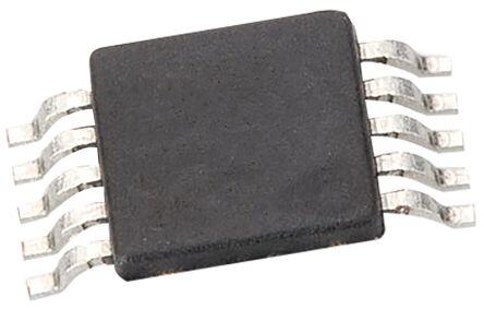
| 供应商器件封装 | 10-VSSOP |
| 其它名称 | 296-29207-2 |
| 分辨率 | 16 bit |
| 制造商产品页 | http://www.ti.com/general/docs/suppproductinfo.tsp?distId=10&orderablePartNumber=ADS1118IDGST |
| 包装 | 剪切带 (CT) |
| 参考设计库 | http://www.digikey.com/rdl/4294959886/4294959871/68 |
| 商标 | Texas Instruments |
| 安装类型 | 表面贴装 |
| 安装风格 | SMD/SMT |
| 封装 | Reel |
| 封装/外壳 | 10-TFSOP,10-MSOP(0.118",3.00mm 宽) |
| 封装/箱体 | VSSOP-10 |
| 工作温度 | -40°C ~ 125°C |
| 工作电源电压 | 2 V to 5.5 V |
| 工厂包装数量 | 250 |
| 接口类型 | Serial SPI |
| 数据接口 | SPI |
| 最大功率耗散 | 0.9 mW |
| 最大工作温度 | + 125 C |
| 最小工作温度 | - 40 C |
| 标准包装 | 250 |
| 特性 | PGA, 温度传感器 |
| 特色产品 | http://www.digikey.com/product-highlights/cn/zh/texas-instruments-ads1118-adc/41 |
| 电压源 | 单电源 |
| 系列 | ADS1118 |
| 结构 | Delta-Sigma |
| 转换器数 | 1 |
| 转换器数量 | 1 |
| 转换速率 | 860 S/s |
| 输入数和类型 | 4 个单端,2 个差分 |
| 输入类型 | Single-Ended/Differential |
| 通道数量 | 4 Channel |
| 采样率(每秒) | 8 ~ 860 |


- 商务部:美国ITC正式对集成电路等产品启动337调查
- 曝三星4nm工艺存在良率问题 高通将骁龙8 Gen1或转产台积电
- 太阳诱电将投资9.5亿元在常州建新厂生产MLCC 预计2023年完工
- 英特尔发布欧洲新工厂建设计划 深化IDM 2.0 战略
- 台积电先进制程称霸业界 有大客户加持明年业绩稳了
- 达到5530亿美元!SIA预计今年全球半导体销售额将创下新高
- 英特尔拟将自动驾驶子公司Mobileye上市 估值或超500亿美元
- 三星加码芯片和SET,合并消费电子和移动部门,撤换高东真等 CEO
- 三星电子宣布重大人事变动 还合并消费电子和移动部门
- 海关总署:前11个月进口集成电路产品价值2.52万亿元 增长14.8%


PDF Datasheet 数据手册内容提取
Product Order Technical Tools & Support & Reference Folder Now Documents Software Community Design ADS1118 SBAS457F–OCTOBER2010–REVISEDSEPTEMBER2019 ADS1118 Ultrasmall, Low-Power, SPI™-Compatible, 16-Bit Analog-to-Digital Converter with Internal Reference and Temperature Sensor 1 Features 3 Description • UltrasmallX2QFNPackage: The ADS1118 is a precision, low power, 16-bit 1 analog-to-digital converter (ADC) that provides all 2mm×1.5mm ×0.4mm features necessary to measure the most common • WideSupplyRange:2Vto5.5V sensor signals in an ultra-small, leadless X2QFN-10 • LowCurrentConsumption: package or a VSSOP-10 package. The ADS1118 – ContinuousMode:Only150 μA integrates a programmable gain amplifier (PGA), voltage reference, oscillator and high-accuracy – Single-ShotMode:AutomaticPowerDown temperature sensor. These features, along with a • ProgrammableDataRate: wide power supply range from 2 V to 5.5 V, make the 8SPSto860SPS ADS1118 ideally suited for power- and space- • Single-CycleSettling constrained,sensor-measurementapplications. • InternalLow-DriftVoltageReference The ADS1118 can perform conversions at data rates upto860samplespersecond(SPS).ThePGA offers • InternalTemperatureSensor: input ranges from ±256 mV to ±6.144 V, allowing 0.5°C(Maximum)Error:0°Cto70°C both large and small signals to be measured with • InternalOscillator high resolution. An input multiplexer (MUX) allows to • InternalPGA measure two differential or four single-ended inputs. • FourSingle-EndedorTwoDifferentialInputs The high-accuracy temperature sensor can be used for system-level temperature monitoring or cold- junctioncompensationforthermocouples. 2 Applications The ADS1118 operates either in continuous- • TemperatureMeasurement: conversion mode, or in a single-shot mode that – ThermocoupleMeasurement automatically powers down after a conversion. – Cold-JunctionCompensation Single-shot mode significantly reduces current consumption during idle periods. Data are transferred – ThermistorMeasurement through a serial peripheral interface (SPI™). The • PortableInstrumentation ADS1118isspecifiedfrom–40°Cto+125°C. • FactoryAutomationandProcessControls DeviceInformation(1) PARTNUMBER PACKAGE BODYSIZE(NOM) X2QFN(10) 1.50mm×2.00mm ADS1118 VSSOP(10) 3.00mm×3.00mm (1) For all available packages, see the orderable addendum at theendofthedatasheet. K-TypeThermocoupleMeasurement UsingIntegratedTemperatureSensorforCold-JunctionCompensation 3.3 V 3.3 V 0.1 (cid:29)F AIN0 VDD ADS1118 Voltage AIN1 Reference SCLK 16-bit Digital Filter CS Mux PGA ß(cid:8)(cid:3) and 3.3 V ADC Interface DOUT/DRDY DIN AIN2 Temperature Oscillator AIN3 Sensor GND 1 An IMPORTANT NOTICE at the end of this data sheet addresses availability, warranty, changes, use in safety-critical applications, intellectualpropertymattersandotherimportantdisclaimers.PRODUCTIONDATA.
ADS1118 SBAS457F–OCTOBER2010–REVISEDSEPTEMBER2019 www.ti.com Table of Contents 1 Features.................................................................. 1 9.4 DeviceFunctionalModes........................................22 2 Applications........................................................... 1 9.5 Programming...........................................................23 3 Description............................................................. 1 9.6 RegisterMaps.........................................................26 4 RevisionHistory..................................................... 2 10 ApplicationandImplementation........................ 28 10.1 ApplicationInformation..........................................28 5 DeviceComparisonTable..................................... 5 10.2 TypicalApplication ...............................................33 6 PinConfigurationandFunctions......................... 5 11 PowerSupplyRecommendations..................... 36 7 Specifications......................................................... 6 11.1 Power-SupplySequencing....................................36 7.1 AbsoluteMaximumRatings......................................6 11.2 Power-SupplyDecoupling.....................................36 7.2 ESDRatings..............................................................6 12 Layout................................................................... 37 7.3 RecommendedOperatingConditions.......................6 12.1 LayoutGuidelines.................................................37 7.4 ThermalInformation..................................................6 12.2 LayoutExample....................................................38 7.5 ElectricalCharacteristics...........................................7 13 DeviceandDocumentationSupport................. 39 7.6 TimingRequirements:SerialInterface......................9 7.7 SwitchingCharacteristics:SerialInterface................9 13.1 DocumentationSupport........................................39 7.8 TypicalCharacteristics............................................10 13.2 ReceivingNotificationofDocumentationUpdates39 13.3 CommunityResources..........................................39 8 ParameterMeasurementInformation................16 13.4 Trademarks...........................................................39 8.1 NoisePerformance.................................................16 13.5 ElectrostaticDischargeCaution............................39 9 DetailedDescription............................................ 17 13.6 Glossary................................................................39 9.1 Overview.................................................................17 14 Mechanical,Packaging,andOrderable 9.2 FunctionalBlockDiagram.......................................17 Information........................................................... 39 9.3 FeatureDescription.................................................18 4 Revision History NOTE:Pagenumbersforpreviousrevisionsmaydifferfrompagenumbersinthecurrentversion. ChangesfromRevisionE(October2015)toRevisionF Page • ChangedmaximumVDDvoltagefrom5.5Vto7VintheAbsoluteMaximumRatingstable............................................... 6 • ChangedbitdescriptionofConfigRegisterbit0.................................................................................................................. 27 ChangesfromRevisionD(October2013)toRevisionE Page • AddedESDRatingstable,FeatureDescriptionsection,NoisePerformancesection,DeviceFunctionalModes section,ApplicationandImplementationsection,PowerSupplyRecommendationssection,Layoutsection,Device andDocumentationSupportsection,andMechanical,Packaging,andOrderableInformationsection .............................. 1 • Changedtitle,Descriptionsection,Featuressection,andblockdiagramonfrontpage....................................................... 1 • ChangedtitlefromProductFamilytoDeviceComparisonTableanddeletedPackageDesignatorcolumn........................5 • UpdateddescriptionsandchangednameofI/OcolumninPinConfigurationsandFunctionstable.................................... 5 • ChangeddigitalinputvoltagerangeandaddedminimumspecificationforT inAbsoluteMaximumRatingstable............6 J • AddedDifferentialinputimpedancespecificationinElectricalCharacteristics...................................................................... 7 • ChangedConditionstatementinTimingRequirements:SerialInterface ............................................................................. 9 • Movedt ,t ,andt parametersfromTimingRequirementstoSwitchingCharacteristics ................................ 9 CSDOD DOPD CSDOZ • Movedt andt valuesfromMINcolumntoMAXcolumn....................................................................................... 9 CSDOD CSDOZ • DeletedNoisevsInputSignal,NoisevsSupplyVoltage,andNoisevsInputSignalplots................................................. 10 • UpdatedOverviewsectionanddeleted"Gain=2/3,1,2,4,8,or16"fromFunctionalBlockDiagram ............................. 17 • UpdatedAnalogInputssection............................................................................................................................................. 19 • UpdatedFull-ScaleRange(FSR)andLSBSizesection..................................................................................................... 20 • UpdatedResetandPowerUpsection................................................................................................................................. 22 • Updated32-BitDataTransmissionCyclesection................................................................................................................ 25 • UpdatedRegisterMapssection........................................................................................................................................... 26 2 SubmitDocumentationFeedback Copyright©2010–2019,TexasInstrumentsIncorporated ProductFolderLinks:ADS1118
ADS1118 www.ti.com SBAS457F–OCTOBER2010–REVISEDSEPTEMBER2019 • UpdatedApplicationInformationsection.............................................................................................................................. 28 • UpdatedFigure48................................................................................................................................................................ 31 • DeletedThermocoupleMeasurementWithColdJunctionTemperaturesection,andmovedFigure50toTypical Applicationsection................................................................................................................................................................ 33 ChangesfromRevisionC(February2013)toRevisionD Page • Deleteddevicegraphic........................................................................................................................................................... 1 • Changedbit1toNOP0inFigure44.................................................................................................................................... 26 • ChangedNOPbitdescriptioninFigure44:changesbits[2:0]tobits[2:1]andchangedNOPtoNOP[1:0]........................ 27 ChangesfromRevisionB(August2012)toRevisionC Page • Changeddocumenttocurrentstandards............................................................................................................................... 1 • ChangedSingle-ShotModesub-bulletinLowCurrentConsumptionFeaturesbullet........................................................... 1 • ChangedInternalTemperatureSensorFeaturesbullet......................................................................................................... 1 • ChangedDescriptionsection.................................................................................................................................................. 1 • ChangedProductFamilytable............................................................................................................................................... 5 • ChangedFunctioncolumnnameinPinDescriptionstable.................................................................................................... 5 • ChangedAnalogInput,Full-scaleinputvoltagerangeparameterrowinElectricalCharacteristicstable............................. 6 • Changedfootnotes1and2inElectricalCharacteristicstable............................................................................................... 6 • ChangedconditionsforElectricalCharacteristicstable......................................................................................................... 7 • ChangedSystemPerformance,IntegralnonlinearityandGainErrortestconditionsinElectricalCharacteristicstable.......7 • ChangedfirsttwoTemperatureSensor,TemperaturesensoraccuracyparametertestconditionsinElectrical Characteristicstable............................................................................................................................................................... 7 • ChangedPower-SupplyRequirements,SupplycurrentparametertestconditionsinElectricalCharacteristicstable..........8 • Changedfootnote3ofTimingRequirements:SerialInterfaceTimingtable.......................................................................... 9 • UpdatedFigure3.................................................................................................................................................................. 10 • UpdatedFigure9.................................................................................................................................................................. 10 • ChangedtitleofFigure11toFigure14................................................................................................................................ 10 • UpdatedFigure15andFigure33........................................................................................................................................ 11 • ChangedconditionsinFigure21toFigure25..................................................................................................................... 12 • UpdatedFigure20................................................................................................................................................................ 13 • ChangedcommentsinFigure27toFigure31..................................................................................................................... 13 • ChangedOverviewsection................................................................................................................................................... 17 • UpdatedMultiplexersection................................................................................................................................................. 18 • ChangedFull-ScaleInputsection......................................................................................................................................... 20 • ChangedVoltageReferencesection.................................................................................................................................... 20 • ChangedOscillatorsection................................................................................................................................................... 20 • AddedmultiplicationpointstoexampleequationsinConvertingfromDigitalCodestoTemperaturesection....................21 • ChangedSerialInterface,ChipSelect,SerialClock,DataInput,andDataOutputandDataReadysections...................23 • ChangedDataRetrievalsection........................................................................................................................................... 24 • ChangedRegisterssection.................................................................................................................................................. 26 • ChangedAliasing,ResetandPowerUp,OperatingModes,andDutyCyclingforLowPowersections............................ 29 • UpdatedFigure50................................................................................................................................................................ 33 Copyright©2010–2019,TexasInstrumentsIncorporated SubmitDocumentationFeedback 3 ProductFolderLinks:ADS1118
ADS1118 SBAS457F–OCTOBER2010–REVISEDSEPTEMBER2019 www.ti.com ChangesfromRevisionA(July2011)toRevisionB Page • Added(VSSOP)totitlesofFigure20toFigure25.............................................................................................................. 13 • AddedFigure26toFigure31............................................................................................................................................... 14 4 SubmitDocumentationFeedback Copyright©2010–2019,TexasInstrumentsIncorporated ProductFolderLinks:ADS1118
ADS1118 www.ti.com SBAS457F–OCTOBER2010–REVISEDSEPTEMBER2019 5 Device Comparison Table MAXIMUMSAMPLE INPUTCHANNELS RESOLUTION SPECIAL DEVICE RATE Differential PGA INTERFACE (Bits) FEATURES (SPS) (Single-Ended) ADS1118 16 860 2(4) Yes SPI Temperaturesensor ADS1018 12 3300 2(4) Yes SPI Temperaturesensor ADS1115 16 860 2(4) Yes I2C Comparator ADS1114 16 860 1(1) Yes I2C Comparator ADS1113 16 860 1(1) No I2C None ADS1015 12 3300 2(4) Yes I2C Comparator ADS1014 12 3300 1(1) Yes I2C Comparator ADS1013 12 3300 1(1) No I2C None 6 Pin Configuration and Functions RUGPackage DGSPackage 10-PinX2QFN 10-PinVSSOP TopView TopView DIN DIN 10 SCLK 1 10 DIN DOUT/ SCLK 1 9 DRDY DOUT/ CS 2 9 CS 2 8 VDD DRDY GND 3 8 VDD GND 3 7 AIN3 AIN0 4 7 AIN3 AIN0 4 6 AIN2 AIN1 5 6 AIN2 5 AIN1 AIN1 PinFunctions PIN TYPE DESCRIPTION NO. NAME 1 SCLK Digitalinput Serialclockinput 2 CS Digitalinput Chipselect;activelow.ConnecttoGNDifnotused. 3 GND Supply Ground 4 AIN0 Analoginput Analoginput0.LeaveunconnectedortietoVDDifnotused. 5 AIN1 Analoginput Analoginput1.LeaveunconnectedortietoVDDifnotused. 6 AIN2 Analoginput Analoginput2.LeaveunconnectedortietoVDDifnotused. 7 AIN3 Analoginput Analoginput3.LeaveunconnectedortietoVDDifnotused. 8 VDD Supply Powersupply.Connecta100-nFpowersupplydecouplingcapacitortoGND. 9 DOUT/DRDY Digitaloutput Serialdataoutputcombinedwithdataready;activelow 10 DIN Digitalinput Serialdatainput Copyright©2010–2019,TexasInstrumentsIncorporated SubmitDocumentationFeedback 5 ProductFolderLinks:ADS1118
ADS1118 SBAS457F–OCTOBER2010–REVISEDSEPTEMBER2019 www.ti.com 7 Specifications 7.1 Absolute Maximum Ratings overoperatingambienttemperaturerange(unlessotherwisenoted)(1) MIN MAX UNIT Power-supplyvoltage VDDtoGND –0.3 7 V Analoginputvoltage AIN0,AIN1,AIN2,AIN3 GND–0.3 VDD+0.3 V Digitalinputvoltage DIN,DOUT/DRDY,SCLK,CS GND–0.3 VDD+0.3 V Inputcurrent,continuous Anypinexceptpowersupplypins –10 10 mA Junction,T –40 150 J Temperature °C Storage,T –60 150 stg (1) StressesbeyondthoselistedunderAbsoluteMaximumRatingsmaycausepermanentdamagetothedevice.Thesearestressratings only,whichdonotimplyfunctionaloperationofthedeviceattheseoranyotherconditionsbeyondthoseindicatedunderRecommended OperatingConditions.Exposuretoabsolute-maximum-ratedconditionsforextendedperiodsmayaffectdevicereliability. 7.2 ESD Ratings VALUE UNIT Electrostatic Human-bodymodel(HBM),perANSI/ESDA/JEDECJS-001(1) ±4000 V V (ESD) discharge Charged-devicemodel(CDM),perJEDECspecificationJESD22-C101(2) ±1000 (1) JEDECdocumentJEP155statesthat500-VHBMallowssafemanufacturingwithastandardESDcontrolprocess. (2) JEDECdocumentJEP157statesthat250-VCDMallowssafemanufacturingwithastandardESDcontrolprocess. 7.3 Recommended Operating Conditions overoperatingambienttemperaturerange(unlessotherwisenoted) MIN NOM MAX UNIT POWERSUPPLY VDD Powersupply VDDtoGND 2 5.5 V ANALOGINPUTS(1) FSR Full-scaleinputvoltagerange(2) V =V -V SeeTable3 IN (AINP) (AINN) V Absoluteinputvoltage GND VDD V (AINx) DIGITALINPUTS Inputvoltage GND VDD V TEMPERATURERANGE T Operatingambienttemperature –40 125 °C A (1) AINPandAINNdenotetheselectedpositiveandnegativeinputs.AINxdenotesoneofthefouravailableanaloginputs. (2) Thisparameterexpressesthefull-scalerangeoftheADCscaling.NomorethanVDD+0.3Vor5.5V(whicheverissmaller)mustbe appliedtothisdevice. 7.4 Thermal Information ADS1118 THERMALMETRIC(1) DGS(VSSOP) RUG(X2QFN) UNIT 10PINS 10PINS R Junction-to-ambientthermalresistance 186.8 245.2 °C/W θJA R Junction-to-case(top)thermalresistance 51.5 69.3 °C/W θJC(top) R Junction-to-boardthermalresistance 108.4 172 °C/W θJB ψ Junction-to-topcharacterizationparameter 2.7 8.2 °C/W JT ψ Junction-to-boardcharacterizationparameter 106.5 170.8 °C/W JB R Junction-to-case(bottom)thermalresistance n/a n/a °C/W θJC(bot) (1) Formoreinformationabouttraditionalandnewthermalmetrics,seetheSemiconductorandICPackageThermalMetricsapplication report. 6 SubmitDocumentationFeedback Copyright©2010–2019,TexasInstrumentsIncorporated ProductFolderLinks:ADS1118
ADS1118 www.ti.com SBAS457F–OCTOBER2010–REVISEDSEPTEMBER2019 7.5 Electrical Characteristics MaximumandminimumspecificationsapplyfromT =–40°Cto+125°C.TypicalspecificationsareatT =25°C. A A AllspecificationsareatVDD=3.3V,datarate=8SPS,andfull-scalerange(FSR)=±2.048V(unlessotherwisenoted). PARAMETER TESTCONDITIONS MIN TYP MAX UNIT ANALOGINPUTS FSR=±6.144V(1) 8 FSR=±4.096V(1),FSR=±2.048V 6 Common-modeinputimpedance MΩ FSR=±1.024V 3 FSR=±0.512V,FSR=±0.256V 100 FSR=±6.144V(1) 22 FSR=±4.096V(1) 15 MΩ Differentialinputimpedance FSR=±2.048V 4.9 FSR=±1.024V 2.4 FSR=±0.512V,FSR=±0.256V 710 kΩ SYSTEMPERFORMANCE Resolution(Nomissingcodes) 16 Bits DR Datarate 8,16,32,64,128,250,475,860 SPS Dataratevariation Alldatarates –10% 10% Outputnoise SeeNoisePerformancesection INL Integralnonlinearity DR=8SPS,FSR=±2.048V(2) 1 LSB FSR=±2.048V,differentialinputs ±0.1 ±2 Offseterror LSB FSR=±2.048V,single-endedinputs ±0.25 Offsetdrift FSR=±2.048V 0.002 LSB/°C Offsetpower-supplyrejection FSR=±2.048V,DCsupplyvariation 0.2 LSB/V Offsetchannelmatch Matchbetweenanytwoinputs 0.6 LSB Gainerror(3) FSR=±2.048V,T =25°C 0.01% 0.15% A FSR=±0.256V 7 Gaindrift(3)(4) FSR=±2.048V 5 40 ppm/°C FSR=±6.144V(1) 5 Gainpower-supplyrejection 10 ppm/V Gainmatch(3) Matchbetweenanytwogains 0.01% 0.1% Gainchannelmatch Matchbetweenanytwoinputs 0.01% 0.1% AtDC,FSR=±0.256V 105 AtDC,FSR=±2.048V 100 CMRR Common-moderejectionratio AtDC,FSR=±6.144V(1) 90 dB f =50Hz,DR=860SPS 105 CM f =60Hz,DR=860SPS 105 CM TEMPERATURESENSOR Temperaturerange –40 125 °C Temperatureresolution 0.03125 °C/LSB T =0°Cto70°C 0.2 ±0.5 A °C Accuracy T =–40°Cto+125°C 0.4 ±1 A vssupply 0.03125 ±0.25 °C/V (1) Thisparameterexpressesthefull-scalerangeoftheADCscaling.NomorethanVDD+0.3Vor5.5V(whicheverissmaller)mustbe appliedtothisdevice. (2) Best-fitINL;covers99%offull-scale. (3) IncludesallerrorsfromonboardPGAandvoltagereference. (4) Maximumvaluespecifiedbycharacterization. Copyright©2010–2019,TexasInstrumentsIncorporated SubmitDocumentationFeedback 7 ProductFolderLinks:ADS1118
ADS1118 SBAS457F–OCTOBER2010–REVISEDSEPTEMBER2019 www.ti.com Electrical Characteristics (continued) MaximumandminimumspecificationsapplyfromT =–40°Cto+125°C.TypicalspecificationsareatT =25°C. A A AllspecificationsareatVDD=3.3V,datarate=8SPS,andfull-scalerange(FSR)=±2.048V(unlessotherwisenoted). PARAMETER TESTCONDITIONS MIN TYP MAX UNIT DIGITALINPUTS/OUTPUTS V High-levelinputvoltage 0.7VDD VDD V IH V Low-levelinputvoltage GND 0.2VDD V IL V High-leveloutputvoltage I =1mA 0.8VDD V OH OH V Low-leveloutputvoltage I =1mA GND 0.2VDD V OL OL I Inputleakage,high V =5.5V –10 10 μA H IH I Inputleakage,low V =GND –10 10 μA L IL POWERSUPPLY Powerdown,T =25°C 0.5 2 A Powerdown 5 I Supplycurrent μA VDD Operating,T =25°C 150 200 A Operating 300 VDD=5V 0.9 P Powerdissipation VDD=3.3V 0.5 mW D VDD=2V 0.3 8 SubmitDocumentationFeedback Copyright©2010–2019,TexasInstrumentsIncorporated ProductFolderLinks:ADS1118
ADS1118 www.ti.com SBAS457F–OCTOBER2010–REVISEDSEPTEMBER2019 7.6 Timing Requirements: Serial Interface OveroperatingambienttemperaturerangeandVDD=2Vto5.5V(unlessotherwisenoted) MIN MAX UNIT t Delaytime,CSfallingedgetofirstSCLKrisingedge(1) 100 ns CSSC t Delaytime,finalSCLKfallingedgetoCSrisingedge 100 ns SCCS t Pulseduration,CShigh 200 ns CSH t SCLKperiod 250 ns SCLK t Pulseduration,SCLKhigh 100 ns SPWH 100 ns t Pulseduration,SCLKlow(2) SPWL 28 ms t Setuptime,DINvalidbeforeSCLKfallingedge 50 ns DIST t Holdtime,DINvalidafterSCLKfallingedge 50 ns DIHD t Holdtime,SCLKrisingedgetoDOUTinvalid 0 ns DOHD (1) CScanbetiedlowpermanentlyincasetheserialbusisnotsharedwithanyotherdevice. (2) HoldingSCLKlowlongerthan28msresetstheSPIinterface. 7.7 Switching Characteristics: Serial Interface Overoperatingambienttemperaturerange(unlessotherwisenoted) PARAMETER TESTCONDITIONS MIN TYP MAX UNIT Propagationdelaytime, t DOUTload=20pF||100kΩtoGND 100 ns CSDOD CSfallingedgetoDOUTdriven Propagationdelaytime, t DOUTload=20pF||100kΩtoGND 0 50 ns DOPD SCLKrisingedgetovalidnewDOUT Propagationdelaytime, t DOUTload=20pF||100kΩtoGND 100 ns CSDOZ CSrisingedgetoDOUThighimpedance t CS CSH tCSSC tSCLK tSPWH tSCCS SCLK tDIST tDIHD tSPWL tSCSC DIN t t t DOHD t CSDOD DOPD CSDOZ Hi-Z Hi-Z DOUT Figure1. SerialInterfaceTiming Copyright©2010–2019,TexasInstrumentsIncorporated SubmitDocumentationFeedback 9 ProductFolderLinks:ADS1118
ADS1118 SBAS457F–OCTOBER2010–REVISEDSEPTEMBER2019 www.ti.com 7.8 Typical Characteristics AtT =25°C,VDD=3.3V,FSR=±2.048V(unlessotherwisenoted). A 4 4 VDD = 2.0 V 3 3 VDD = 3.3 V VDD = 5.0 V 2 %) 2 Error (mV) 10 Rate Error ( 01 otal -1 ata −1 T D −2 -2 −3 -3 −4 -4 −60 −40 −20 0 20 40 60 80 100 120 140 -2.048 -1.024 0 1.024 2.048 Temperature (°C) G028 Input Signal (V) DR=860SPS,diffinputs,includesnoise,offsetandgainerror Figure2.TotalErrorvsInputSignal Figure3.DataRatevsTemperature 15 5 FSR = ±0.256 V T =−40°C 4 A FSR = ±0.512 V T =25°C 12.5 A m) FSR = ±2.048 V m) 3 TA=125°C Nonlinearity (pp 71.50 FSR = ±6.144 V Nonlinearity (pp −1012 Integral 2.55 Integral −−32 −4 0 −5 2.0 2.5 3.0 3.5 4.0 4.5 5.0 5.5 −2 −1.5 −1 −0.5 0 0.5 1 1.5 2 Supply Voltage (V) G010 Input Signal (V) FSR=±2.048V,DR=8SPS,VDD=3.3V,bestfit Figure4.INLvsSupplyVoltage Figure5.INLvsInputSignal 10 5 T =−40°C T =−40°C 8 A 4 A T =25°C T =25°C A A m) 6 TA=125°C m) 3 TA=125°C p p y (p 4 y (p 2 arit 2 arit 1 e e n 0 n 0 nli nli No −2 No −1 gral −4 gral −2 e e nt −6 nt −3 I I −8 −4 −10 −5 −0.5 −0.4 −0.2 −0.1 0 0.1 0.2 0.4 0.5 −2 −1.5 −1 −0.5 0 0.5 1 1.5 2 Input Signal (V) Input Signal (V) FSR=±0.512V,DR=8SPS,VDD=3.3V,bestfit FSR=±2.048V,DR=8SPS,VDD=5V,bestfit Figure6.INLvsInputSignal Figure7.INLvsInputSignal 10 SubmitDocumentationFeedback Copyright©2010–2019,TexasInstrumentsIncorporated ProductFolderLinks:ADS1118
ADS1118 www.ti.com SBAS457F–OCTOBER2010–REVISEDSEPTEMBER2019 Typical Characteristics (continued) AtT =25°C,VDD=3.3V,FSR=±2.048V(unlessotherwisenoted). A 10 12 8 TA=−40°C VDD = 2.0 V TA=25°C 10 VDD = 3.3 V m) 6 TA=125°C m) VDD = 5.0 V p p y (p 4 y (p 8 arit 2 arit e e nlin 0 nlin 6 No −2 No gral −4 gral 4 e e nt −6 nt I I 2 −8 −10 0 −0.5 −0.4 −0.2 −0.1 0 0.1 0.2 0.4 0.5 −60 −40 −20 0 20 40 60 80 100 120 140 Input Signal (V) Temperature (°C) G015 FSR=±0.512V,DR=8SPS,VDD=5V,bestfit FSR=±2.048V,DR=8SPS,bestfit Figure8.INLvsInputSignal Figure9.INLvsTemperature 16 60 T =−40°C AIN0 to GND A 14 T =25°C AIN1 to GND A 40 arity (ppm) 1102 TA=125°C ge (µV) 20 AAIINN23 ttoo GGNNDD e a nlin 8 Volt 0 No 6 et egral 4 Offs −20 Int −40 2 0 −60 88 1166 3322 6644 112288 225500 447755 886600 −40 −20 0 20 40 60 80 100 120 Data Rate (SPS) Temperature (°C) G004 FSR=±2.048V,bestfit Figure10.INLvsDataRate Figure11.Single-EndedOffsetVoltagevsTemperature 60 40 AIN0 to GND AIN0 toAIN1 AIN1 to GND 30 AIN0 toAIN3 40 AIN2 to GND AIN1 toAIN3 µV) 20 AIN3 to GND µV) 20 AIN2 toAIN3 e ( e ( 10 g g a a olt 0 olt 0 V V et et −10 Offs −20 Offs −20 −40 −30 −60 −40 2 2.5 3 3.5 4 4.5 5 −40 −20 0 20 40 60 80 100 120 Supply Voltage (V) Temperature (°C) G005 G006 Figure12.Single-EndedOffsetVoltagevsSupply Figure13.DifferentialOffsetVoltagevsTemperature Copyright©2010–2019,TexasInstrumentsIncorporated SubmitDocumentationFeedback 11 ProductFolderLinks:ADS1118
ADS1118 SBAS457F–OCTOBER2010–REVISEDSEPTEMBER2019 www.ti.com Typical Characteristics (continued) AtT =25°C,VDD=3.3V,FSR=±2.048V(unlessotherwisenoted). A 40 15 AIN0 toAIN1 30 AIN0 toAIN3 AIN1 toAIN3 s Voltage (µV) 12000 AIN2 toAIN3 of Occurrence 10 Offset −−2100 Number 5 −30 0 −40 2 2.5 3 3.5 4 4.5 5 55 44 33 22 11 00 11 22 33 44 55 00 00 00 00 00 00 00 00 00 00 Supply Voltage (V) G007 −0.0−0.0 −0.0−0.0 −0.0−0.0 −0.0−0.0 −0.0−0.0 0.00.0 0.00.0 0.00.0 0.00.0 0.00.0 Offset Drift (LSB/°C) G046 FSR=±2.048V,T =–40°Cto+125°C,MUX=AIN0toAIN3, A 540unitsfrom3productionlots Figure14.DifferentialOffsetVoltagevsSupply Figure15.OffsetDriftHistogram 200 0.05 0.04 es 150 0.03 c n 0.02 mber of Occurre 100 Gain Error (%) −00..00101 FFSSRR == ±±00..255162 VV Nu 50 −0.02 FSR = ±1.024 V −0.03 FSR = ±2.048 V FSR = ±4.096 V −0.04 FSR = ±6.144 V 0 −0.05 0088664422002244668800224466880022446688 −1−1−−−−−−−− 11111111112222222222 −40 −20 0 20 40 60 80 100 120 140 Offset (µV) Temperature (°C) G000 FSR=±2.048V, 540unitsfrom3productionlots Figure16.OffsetHistogram Figure17.GainErrorvsTemperature 0.15 200 0.1 es 150 c n Error (%) 0.050 FFSSRR ==±±22.5064 8m VV of Occurren 100 Gai -0.05 ber m u 50 N -0.1 -0.15 0 2 2.5 3 3.5 4 4.5 5 5.5 22 55 11 55 00 55 11 55 22 55 33 55 44 55 55 00 11 00 00 00 00 11 00 22 00 33 00 44 00 Supply Voltage (V) −0−0.. 00.0.0 −0.−0. 0.00.0 0.00.0 0.0. 0.0.00 0.0. 0.0.00 0.0. 0.00.0 0.0. 0.00.0 0.0. −− −− Gain Error (%) G000 FSR=±2.048V, 540unitsfrom3productionlots Figure18.GainErrorvsSupply Figure19.GainErrorHistogram 12 SubmitDocumentationFeedback Copyright©2010–2019,TexasInstrumentsIncorporated ProductFolderLinks:ADS1118
ADS1118 www.ti.com SBAS457F–OCTOBER2010–REVISEDSEPTEMBER2019 Typical Characteristics (continued) AtT =25°C,VDD=3.3V,FSR=±2.048V(unlessotherwisenoted). A 1 40 Average Temperature Error 0.8 Average ± 3 sigma 35 0.6 Average ± 6 sigma or (°C) 0.4 nces 30 Err 0.2 ure 25 ure 0 Occ 20 perat −0.2 er of 15 m −0.4 b e m T −0.6 Nu 10 −0.8 5 −1 −40 −20 0 20 40 60 80 100 120 0 Temperature (°C) G023 0.5 0.4 0.3 0.2 0.1 0 0.1 0.2 0.3 0.4 0.5 - - - - - Temperature Error (qC) T =–40°C,48unitsfrom3productionlots A Figure20.TemperatureSensorErrorvsTemp(VSSOP) Figure21.TemperatureSensorErrorHistogram(VSSOP) 40 40 35 35 s 30 s 30 e e c c n n ure 25 ure 25 c c c c O 20 O 20 of of er 15 er 15 b b m m u u N 10 N 10 5 5 0 0 5 4 3 2 1 0 1 2 3 4 5 5 4 3 2 1 0 1 2 3 4 5 0. 0. 0. 0. 0. 0. 0. 0. 0. 0. 0. 0. 0. 0. 0. 0. 0. 0. 0. 0. - - - - - - - - - - Temperature Error (qC) Temperature Error (qC) T =0°C,48unitsfrom3productionlots T =25°C,48unitsfrom3productionlots A A Figure22.TemperatureSensorErrorHistogram(VSSOP) Figure23.TemperatureSensorErrorHistogram(VSSOP) 40 40 35 35 s 30 s 30 e e c c n n ure 25 ure 25 c c c c O 20 O 20 of of er 15 er 15 b b m m u u N 10 N 10 5 5 0 0 5 4 3 2 1 0 1 2 3 4 5 5 4 3 2 1 0 1 2 3 4 5 0. 0. 0. 0. 0. 0. 0. 0. 0. 0. 0. 0. 0. 0. 0. 0. 0. 0. 0. 0. - - - - - - - - - - Temperature Error (qC) Temperature Error (qC) T =70°C,48unitsfrom3productionlots T =125°C,48unitsfrom3productionlots A A Figure24.TemperatureSensorErrorHistogram(VSSOP) Figure25.TemperatureSensorErrorHistogram(VSSOP) Copyright©2010–2019,TexasInstrumentsIncorporated SubmitDocumentationFeedback 13 ProductFolderLinks:ADS1118
ADS1118 SBAS457F–OCTOBER2010–REVISEDSEPTEMBER2019 www.ti.com Typical Characteristics (continued) AtT =25°C,VDD=3.3V,FSR=±2.048V(unlessotherwisenoted). A 1 70 Average Temperature Error 0.8 Average (cid:147) 3 sigma 60 C) 0.6 Average (cid:147) 6 sigma (cid:131)or ( 0.4 nces 50 ure Err 0.20 Occure 40 perat -0.2 er of 30 m -0.4 b Te um 20 -0.6 N -0.8 10 -1 -40 -20 0 20 40 60 80 100 120 0 Temperature ((cid:131)C) C007 0.5 0.4 0.3 0.2 0.1 0 0.1 0.2 0.3 0.4 0.5 - - - - - Temperature Error (qC) T =–40°C,94unitsfromproduction A Figure26.TemperatureSensorErrorvsTemp(X2QFN) Figure27.TemperatureSensorErrorHistogram(X2QFN) 70 70 60 60 s s e 50 e 50 c c n n e e cur 40 cur 40 c c O O er of 30 er of 30 b b m m u 20 u 20 N N 10 10 0 0 5 4 3 2 1 0 1 2 3 4 5 5 4 3 2 1 0 1 2 3 4 5 0. 0. 0. 0. 0. 0. 0. 0. 0. 0. 0. 0. 0. 0. 0. 0. 0. 0. 0. 0. - - - - - - - - - - Temperature Error (qC) Temperature Error (qC) T =0°C,94unitsfromproduction T =25°C,94unitsfromproduction A A Figure28.TemperatureSensorErrorHistogram(X2QFN) Figure29.TemperatureSensorErrorHistogram(X2QFN) 70 70 60 60 s s e 50 e 50 c c n n e e cur 40 cur 40 c c O O er of 30 er of 30 b b m m u 20 u 20 N N 10 10 0 0 5 4 3 2 1 0 1 2 3 4 5 5 4 3 2 1 0 1 2 3 4 5 0. 0. 0. 0. 0. 0. 0. 0. 0. 0. 0. 0. 0. 0. 0. 0. 0. 0. 0. 0. - - - - - - - - - - Temperature Error (qC) Temperature Error (qC) T =70°C,94unitsfromproduction T =125°C,94unitsfromproduction A A Figure30.TemperatureSensorErrorHistogram(X2QFN) Figure31.TemperatureSensorErrorHistogram(X2QFN) 14 SubmitDocumentationFeedback Copyright©2010–2019,TexasInstrumentsIncorporated ProductFolderLinks:ADS1118
ADS1118 www.ti.com SBAS457F–OCTOBER2010–REVISEDSEPTEMBER2019 Typical Characteristics (continued) AtT =25°C,VDD=3.3V,FSR=±2.048V(unlessotherwisenoted). A 300 5 VDD = 2.0 V 4.5 VDD = 3.3 V 250 A) VDD= 5 V µA) 4 VDD = 5.0 V nt (m 200 ent ( 3.5 g Curre 150 VDD= 3.3 V wn Curr 2.35 peratin 100 VDD= 2 V er−Do 1.25 O w 50 Po 1 0.5 0 0 -40 -20 0 20 40 60 80 100 120 140 −40 −20 0 20 40 60 80 100 120 140 Temperature (°C) Temperature (°C) G003 Figure32.OperatingCurrentvsTemperature Figure33.Power-DownCurrentvsTemperature 0 -10 -20 -30 B) d n ( -40 ai G -50 -60 -70 -80 1 10 100 1k 10k Input Frequency (Hz) DR=8SPS Figure34.DigitalFilterFrequencyResponse Copyright©2010–2019,TexasInstrumentsIncorporated SubmitDocumentationFeedback 15 ProductFolderLinks:ADS1118
ADS1118 SBAS457F–OCTOBER2010–REVISEDSEPTEMBER2019 www.ti.com 8 Parameter Measurement Information 8.1 Noise Performance Delta-sigma (ΔΣ) analog-to-digital converters (ADCs) are based on the principle of oversampling. The input signal of a ΔΣ ADC is sampled at a high frequency (modulator frequency) and subsequently filtered and decimated in the digital domain to yield a conversion result at the respective output data rate. The ratio between modulator frequency and output data rate is called oversampling ratio (OSR). By increasing the OSR, and thus reducing the output data rate, the noise performance of the ADC can be optimized. In other words, the input- referred noise drops when reducing the output data rate because more samples of the internal modulator are averaged to yield one conversion result. Increasing the gain also reduces the input-referred noise, which is particularlyusefulwhenmeasuringlow-levelsignals. Table 1 and Table 2 summarize the device noise performance. Data are representative of typical noise performance at T = 25°C with the inputs shorted together externally. Table 1 show the input-referred noise in A units of μV for the conditions shown. Note that µV values are shown in parenthesis. Table 2 shows the RMS PP corresponding data in effective number of bits (ENOB) calculated from μV values using Equation 1. The RMS noise-freebitscalculatedfrompeak-to-peaknoisevaluesusingEquation2 areshowninparenthesis. ENOB=ln(FSR/V )/ln(2) (1) RMS-Noise Noise-FreeBits=ln(FSR/V )/ln(2) (2) PP-Noise Table1.NoiseinμV (μV )atVDD=3.3V RMS PP FSR(Full-ScaleRange) DATARATE (SPS) ±6.144V ±4.096V ±2.048V ±1.024V ±0.512V ±0.256V 8 187.5(187.5) 125(125) 62.5(62.5) 31.25(31.25) 15.62(15.62) 7.81(7.81) 16 187.5(187.5) 125(125) 62.5(62.5) 31.25(31.25) 15.62(15.62) 7.81(7.81) 32 187.5(187.5) 125(125) 62.5(62.5) 31.25(31.25) 15.62(15.62) 7.81(7.81) 64 187.5(187.5) 125(125) 62.5(62.5) 31.25(31.25) 15.62(15.62) 7.81(7.81) 128 187.5(187.5) 125(125) 62.5(62.5) 31.25(31.25) 15.62(15.62) 7.81(12.35) 250 187.5(252.09) 125(148.28) 62.5(84.03) 31.25(39.54) 15.62(16.06) 7.81(18.53) 475 187.5(266.92) 125(227.38) 62.5(79.08) 31.25(56.84) 15.62(32.13) 7.81(25.95) 860 187.5(430.06) 125(266.93) 62.5(118.63) 31.25(64.26) 15.62(40.78) 7.81(35.83) Table2.ENOBfromRMSNoise(Noise-FreeBitsfromPeak-to-PeakNoise)atVDD=3.3V FSR(Full-ScaleRange) DATARATE (SPS) ±6.144V ±4.096V ±2.048V ±1.024V ±0.512V ±0.256V 8 16(16) 16(16) 16(16) 16(16) 16(16) 16(16) 16 16(16) 16(16) 16(16) 16(16) 16(16) 16(16) 32 16(16) 16(16) 16(16) 16(16) 16(16) 16(16) 64 16(16) 16(16) 16(16) 16(16) 16(16) 16(16) 128 16(16) 16(16) 16(16) 16(16) 16(16) 16(15.33) 250 16(15.57) 16(15.75) 16(15.57) 16(15.66) 16(15.96) 16(14.75) 475 16(15.49) 16(15.13) 16(15.66) 16(15.13) 16(14.95) 16(14.26) 860 16(14.8) 16(14.9) 16(15.07) 16(14.95) 16(14.61) 16(13.8) 16 SubmitDocumentationFeedback Copyright©2010–2019,TexasInstrumentsIncorporated ProductFolderLinks:ADS1118
ADS1118 www.ti.com SBAS457F–OCTOBER2010–REVISEDSEPTEMBER2019 9 Detailed Description 9.1 Overview The ADS1118 is a very small, low-power, 16-bit, delta-sigma (ΔΣ) analog-to-digital converter (ADC). The ADS1118 consists of a ΔΣ ADC core with adjustable gain, an internal voltage reference, a clock oscillator, and an SPI. This device is also a highly linear and accurate temperature sensor. All of these features are intended to reduce required external circuitry and improve performance. Functional Block Diagram shows the ADS1118 functionalblockdiagram. The ADS1118 ADC core measures a differential signal, V , that is the difference of V and V . The IN (AINP) (AINN) converter core consists of a differential, switched-capacitor ΔΣ modulator followed by a digital filter. This architecture results in a very strong attenuation in any common-mode signals. Input signals are compared to the internal voltage reference. The digital filter receives a high-speed bitstream from the modulator and outputs a codeproportionaltotheinputvoltage. The ADS1118 has two available conversion modes: single-shot mode and continuous conversion mode. In single-shot mode, the ADC performs one conversion of the input signal upon request and stores the value to an internal conversion register. The device then enters a power-down state. This mode is intended to provide significant power savings in systems that require only periodic conversions or when there are long idle periods between conversions. In continuous conversion mode, the ADC automatically begins a conversion of the input signal as soon as the previous conversion is completed. The rate of continuous conversion is equal to the programmeddatarate.Datacanbereadatanytimeandalwaysreflectthemostrecentlycompletedconversion. 9.2 Functional Block Diagram VDD Device Voltage Reference Mux CS AIN0 SCLK Serial 16-BitΔΣ AIN1 PGA Peripheral DIN ADC Interface DOUT/DRDY AIN2 Temperature Oscillator Sensor AIN3 GND Copyright©2010–2019,TexasInstrumentsIncorporated SubmitDocumentationFeedback 17 ProductFolderLinks:ADS1118
ADS1118 SBAS457F–OCTOBER2010–REVISEDSEPTEMBER2019 www.ti.com 9.3 Feature Description 9.3.1 Multiplexer The ADS1118 contains an input multiplexer (mux), as shown in Figure 35. Either four single-ended or two differential signals can be measured. Additionally, AIN0, AIN1, and AIN2 can be measured differentially to AIN3. The multiplexer is configured by bits MUX[2:0] in the Config register. When single-ended signals are measured, thenegativeinputoftheADCisinternallyconnectedtoGNDbyaswitchwithinthemultiplexer. VDD Device AIN0 VDD GND AIN P AIN1 AIN N VDD GND AIN2 VDD GND AIN3 GND GND Figure35. InputMultiplexer When measuring single-ended inputs, the device does not output negative codes. These negative codes indicate negative differential signals; that is, (V – V ) < 0. Electrostatic discharge (ESD) diodes to VDD and GND (AINP) (AINN) protect the ADS1118 inputs. To prevent the ESD diodes from turning on, keep the absolute voltage on any input withintherangegiveninEquation3: GND–0.3V<V <VDD+0.3V (3) (AINx) If the voltages on the input pins can possibly violate these conditions, use external Schottky diodes and series resistorstolimittheinputcurrenttosafevalues(seetheAbsoluteMaximumRatingstable). Also, overdriving one unused input on the ADS1118 may affect conversions currently taking place on other input pins.Ifoverdrivingunusedinputsispossible,clampthesignalwithexternalSchottkydiodes. 18 SubmitDocumentationFeedback Copyright©2010–2019,TexasInstrumentsIncorporated ProductFolderLinks:ADS1118
ADS1118 www.ti.com SBAS457F–OCTOBER2010–REVISEDSEPTEMBER2019 Feature Description (continued) 9.3.2 AnalogInputs The ADS1118 uses a switched-capacitor input stage where capacitors are continuously charged and then discharged to measure the voltage between AIN and AIN . This frequency at which the input signal is sampled P N is called the sampling frequency or the modulator frequency (f ). ADS1118 has a 1 MHz internal oscillator (MOD) which is further divided by a factor of 4 to generate the modulator frequency at 250 kHz. The capacitors used in thisinputstagearesmall,andto external circuitry, the average loading appears resistive. This structure is shown in Figure 36. The resistance is set by the capacitor values and the rate at which they are switched. Figure 37 shows the setting of the switches illustrated in Figure 36. During the sampling phase, switches S are closed. 1 This event charges C to V , C to V , and C to (V – V ). During the discharge phase, S is A1 (AINP) A2 (AINN) B (AINP) (AINN) 1 firstopenedandthenS isclosed.BothC andC thendischarge to approximately 0.7 V and C discharges to 2 A1 A2 B 0 V. This charging draws a very small transient current from the source driving the ADS1118 analog inputs. The averagevalueofthiscurrentcanbeusedtocalculatetheeffectiveimpedance(Z ),whereZ =V /I . eff eff IN AVERAGE 0.7 V C A1 Z CM AIN 0.7 V Equivalent P S1 S2 Circuit AINP C B Z DIFF S S 1 2 AINN 0.7 V AINN CA2 f = 250 kHz ZCM (MOD) 0.7 V Figure36. SimplifiedAnalogInputCircuit t SAMPLE ON S 1 OFF ON S 2 OFF Figure37. S andS SwitchTiming 1 2 The common-mode input impedance is measured by applying a common-mode signal to the shorted AIN and P AIN inputs and measuring the average current consumed by each pin. The common-mode input impedance N changes depending on the full-scale range, but is approximately 6 MΩ for the default full-scale range. In Figure36,thecommon-modeinputimpedanceisZ . CM The differential input impedance is measured by applying a differential signal to AIN and AIN inputs where one P N input is held at 0.7 V. The current that flows through the pin connected to 0.7 V is the differential current and scaleswiththefull-scalerange.InFigure36,thedifferentialinputimpedanceisZ . DIFF Make sure to consider the typical value of the input impedance. Unless the input source has a low impedance, the ADS1118 input impedance may affect the measurement accuracy. For sources with high-output impedance, buffering may be necessary. Active buffers introduce noise, and also introduce offset and gain errors. Consider allofthesefactorsinhigh-accuracyapplications. The clock oscillator frequency drifts slightly with temperature; therefore, the input impedances also drift. For most applications,thisinputimpedancedriftisnegligible,andcanbeignored. Copyright©2010–2019,TexasInstrumentsIncorporated SubmitDocumentationFeedback 19 ProductFolderLinks:ADS1118
ADS1118 SBAS457F–OCTOBER2010–REVISEDSEPTEMBER2019 www.ti.com Feature Description (continued) 9.3.3 Full-ScaleRange(FSR)andLSBSize A programmable gain amplifier (PGA) is implemented before the ADS1118 ΔΣ core. The full-scale range is configured by three bits (PGA[2:0]) in the Config Register and can be set to ±6.144 V, ±4.096 V, ±2.048 V, ±1.024 V, ±0.512 V, ±0.256 V. Table 3 shows the FSR together with the corresponding LSB size. LSB size is calculated from full-scale voltage by the formula shown in Equation 4. However, analog input voltages may never exceed the analog input voltage limits given in the Electrical Characteristics. If a supply voltage of VDD greater than 4 V is used, the ±6.144 V full-scale range allows input voltages to extend up to the supply. Note though that in this case, or whenever the supply voltage is less than the full-scale range (for example, VDD = 3.3 V and full- scale range = ±4.096 V), a full-scale ADC output code cannot be obtained. This inability means that some dynamicrangeislost. LSB=FSR/216 (4) Table3.Full-ScaleRangeandCorrespondingLSBSize FSR LSBSIZE ±6.144V(1) 187.5μV ±4.096V(1) 125μV ±2.048V 62.5μV ±1.024V 31.25μV ±0.512V 15.625μV ±0.256V 7.8125μV (1) Thisparameterexpressesthefull-scalerangeoftheADCscaling. NomorethanVDD+0.3Vmustbeappliedtothisdevice. 9.3.4 VoltageReference The ADS1118 has an integrated voltage reference. An external reference cannot be used with this device. Errors associated with the initial voltage reference accuracy and the reference drift with temperature are included in the gainerrorandgaindriftspecificationsintheElectricalCharacteristics. 9.3.5 Oscillator The ADS1118 has an integrated oscillator running at 1 MHz. No external clock is required to operate the device. Note that the internal oscillator drifts over temperature and time. The output data rate will scale proportional with theoscillatorfrequency. 20 SubmitDocumentationFeedback Copyright©2010–2019,TexasInstrumentsIncorporated ProductFolderLinks:ADS1118
ADS1118 www.ti.com SBAS457F–OCTOBER2010–REVISEDSEPTEMBER2019 9.3.6 TemperatureSensor The ADS1118 offers an integrated precision temperature sensor. The temperature sensor mode is enabled by setting bit TS_MODE = 1 in the Config Register. Temperature data are represented as a 14-bit result that is left- justified within the 16-bit conversion result. Data are output starting with the most significant byte (MSB). When reading the two data bytes, the first 14 bits are used to indicate the temperature measurement result. One 14-bit LSB equals 0.03125°C. Negative numbers are represented in binary twos complement format, as shown in Table4. Table4.14-BitTemperatureDataFormat TEMPERATURE(°C) DIGITALOUTPUT(BINARY) HEX 128 01000000000000 1000 127.96875 00111111111111 0FFF 100 00110010000000 0C80 75 00100101100000 0960 50 00011001000000 0640 25 00001100100000 0320 0.25 00000000001000 0008 0.03125 00000000000001 0001 0 00000000000000 0000 –0.25 11111111111000 3FF8 –25 11110011100000 3CE0 –40 11101100000000 3B00 9.3.6.1 ConvertingfromTemperaturetoDigitalCodes Forpositivetemperatures: Twos complement is not performed on positive numbers. Therefore, simply convert the number to binary codeina14-bit,leftjustifiedformatwiththeMSB=0todenotethepositivesign. Example:50°C/(0.03125°C/count)=1600=0640h=00011001000000 Fornegativetemperatures: Generate the twos complement of a negative number by complementing the absolute binary number and adding1.ThendenotethenegativesignwiththeMSB=1. Example:|–25°C|/(0.03125°C/count)=800=0320h=00001100100000 Twoscomplementformat:11110011011111+1=11110011100000 9.3.6.2 ConvertingfromDigitalCodestoTemperature To convert from digital codes to temperature, first check whether the MSB is a 0 or a 1. If the MSB is a 0, simply multiply the decimal code by 0.03125°C to obtain the result. If the MSB = 1, subtract 1 from the result andcomplementallofthebits.Thenmultiplytheresultby –0.03125°C. Example:Thedevicereadsback0960h:0960hhasanMSB=0. 0960h×0.03125°C=2400 × 0.03125°C=75°C Example:Thedevicereadsback3CE0h:3CE0hhasanMSB=1. Subtract1andcomplementtheresult:3CE0h →0320h 0320h×(–0.03125°C)=800 ×(–0.03125°C)= –25°C Copyright©2010–2019,TexasInstrumentsIncorporated SubmitDocumentationFeedback 21 ProductFolderLinks:ADS1118
ADS1118 SBAS457F–OCTOBER2010–REVISEDSEPTEMBER2019 www.ti.com 9.4 Device Functional Modes 9.4.1 ResetandPowerUp When the ADS1118 powers up, a reset is performed. As part of the reset process, the ADS1118 sets all of its bits in the Config Register to the respective default settings. By default, the ADS1118 enters a power-down state at start-up. The device interface and digital blocks are active, but no data conversions are performed. The initial power-down state of the ADS1118 is intended to relieve systems with tight power-supply requirements from encounteringasurgeduringpowerup. 9.4.2 OperatingModes The ADS1118 operates in one of two modes: continuous-conversion or single-shot. The MODE bit in the Config registerselectstherespectiveoperatingmode. 9.4.2.1 Single-ShotModeandPower-Down When the MODE bit in the Config register is set to 1, the ADS1118 enters a power-down state, and operates in single-shot mode. This power-down state is the default state for the ADS1118 when power is first applied. Althoughpowereddown,thedevicestill responds to commands. The ADS1118 remains in this power-down state until a 1 is written to the single-shot (SS) bit in the Config register. When the SS bit is asserted, the device powers up, resets the SS bit to 0, and starts a single conversion. When conversion data are ready for retrieval, thedevicepowersdownagain.Writing a 1 to the SS bit while a conversion is ongoing has no effect. To switch to continuous-conversionmode,writea0totheMODEbitintheConfigregister. 9.4.2.2 Continuous-ConversionMode In continuous-conversion mode (MODE bit set to 0), the ADS1118 continuously performs conversions. When a conversion completes, the ADS1118 places the result in the Conversion register and immediately begins another conversion.Toswitchtosingle-shotmode,writea1totheMODEbitintheConfigregister,orresetthedevice. 9.4.3 DutyCyclingforLowPower The noise performance of a ΔΣ ADC generally improves when lowering the output data rate because more samples of the internal modulator can be averaged to yield one conversion result. In applications where power consumption is critical, the improved noise performance at low data rates may not be required. For these applications, the ADS1118 supports duty cycling that can yield significant power savings by periodically requesting high data rate readings at an effectively lower data rate. For example, an ADS1118 in power-down state with a data rate set to 860 SPS can be operated by a microcontroller that instructs a single-shot conversion every 125 ms (8 SPS). Because a conversion at 860 SPS only requires approximately 1.2 ms, the ADS1118 enters power-down state for the remaining 123.8 ms. In this configuration, the ADS1118 consumes approximately 1/100th the power that is otherwise consumed in continuous conversion mode. The duty cycling rate is completely arbitrary and is defined by the master controller. The ADS1118 offers lower data rates that do notimplementdutycyclingandalsooffersimprovednoiseperformanceifrequired. 22 SubmitDocumentationFeedback Copyright©2010–2019,TexasInstrumentsIncorporated ProductFolderLinks:ADS1118
ADS1118 www.ti.com SBAS457F–OCTOBER2010–REVISEDSEPTEMBER2019 9.5 Programming 9.5.1 SerialInterface The SPI-compatible serial interface consists of either four signals (CS, SCLK, DIN, and DOUT/DRDY), or three signals (in which case CS may be tied low). The interface is used to read conversion data, read and write registers,andcontroldeviceoperation. 9.5.2 ChipSelect(CS) The chip select pin (CS) selects the ADS1118 for SPI communication. This feature is useful when multiple devices share the same serial bus. Keep CS low for the duration of the serial communication. When CS is taken high,theserialinterfaceisreset,SCLKisignored,andDOUT/DRDYentersahigh-impedancestate.Inthisstate, DOUT/DRDY cannot provide data-ready indication. In situations where multiple devices are present and DOUT/DRDY must be monitored, lower CS periodically. At this point, the DOUT/DRDY pin either immediately goes high to indicate that no new data are available, or immediately goes low to indicate that new data are present in the Conversion register and are available for transfer. New data can be transferred at any time without concern of data corruption. When a transmission starts, the current result is locked into the output shift register anddoesnotchangeuntilthecommunicationcompletes.Thissystemavoidsanypossibilityofdatacorruption. 9.5.3 SerialClock(SCLK) The serial clock (SCLK) features a Schmitt-triggered input and is used to clock data on the DIN and DOUT/DRDY pins into and out of the ADS1118. Even though the input has hysteresis, TI recommends keeping SCLK as clean as possible to prevent glitches from accidentally shifting the data. If SCLK is held low for 28 ms, the serial interface resets and the next SCLK pulse starts a new communication cycle. This time-out feature can be used to recover communication when a serial interface transmission is interrupted. When the serial interface isidle,holdSCLKlow. 9.5.4 DataInput(DIN) The data input pin (DIN) is used along with SCLK to send data to the ADS1118. The device latches data on DIN ontheSCLKfallingedge.TheADS1118neverdrivestheDINpin. 9.5.5 DataOutputandDataReady(DOUT/DRDY) The data output and data ready pin (DOUT/DRDY) is used with SCLK to read conversion and register data from the ADS1118. Data on DOUT/DRDY are shifted out on the SCLK rising edge. DOUT/DRDY is also used to indicate that a conversion is complete and new data are available. This pin transitions low when new data are ready for retrieval. DOUT/DRDY is also able to trigger a microcontroller to start reading data from the ADS1118. In continuous-conversion mode, DOUT/DRDY transitions high again 8 µs before the next data ready signal (DOUT/DRDY low) if no data are retrieved from the device. This transition is shown in Figure 38. Complete the datatransferbeforeDOUT/DRDYreturnshigh. CS(1) SCLK 8 µs Hi-Z DOUT/DRDY DIN (1) CSmaybeheldlow.IfCSislow,DOUT/DRDYassertslowindicatingnewdataareavailable. Figure38. DOUT/DRDYBehaviorWithoutDataRetrievalinContinuousConversionMode When CS is high, DOUT/DRDY is configured by default with a weak internal pullup resistor. This feature reduces the risk of DOUT/DRDY floating near midsupply and causing leakage current in the master device. To disable this pullup resistor and place the device into a high-impedance state, set the PULL_UP_EN bit to 0 in the Config Register. Copyright©2010–2019,TexasInstrumentsIncorporated SubmitDocumentationFeedback 23 ProductFolderLinks:ADS1118
ADS1118 SBAS457F–OCTOBER2010–REVISEDSEPTEMBER2019 www.ti.com Programming (continued) 9.5.6 DataFormat The ADS1118 provides 16 bits of data in binary twos complement format. A positive full-scale input produces an outputcodeof7FFFhandanegativefull-scaleinputproducesanoutputcodeof8000h.Theoutputclipsatthese codes for signals that exceed full-scale. Table 5 summarizes the ideal output codes for different input signals. Figure39showscodetransitionsversusinputvoltage. Table5.InputSignalversusIdealOutputCode INPUTSIGNAL,VIN IDEALOUTPUTCODE(1) (AIN –AIN ) P N ≥+FS(215–1)/215 7FFFh +FS/215 0001h 0 0 –FS/215 FFFFh ≤–FS 8000h (1) Excludestheeffectsofnoise,INL,offset,andgainerrors. 0x7FFF 0x7FFE ¼ e 0x0001 d o C 0x0000 put 0xFFFF ut O ¼ 0x8001 0x8000 ¼ ¼ -FS 0 FS Input Voltage (AIN -AIN ) P N 215-1 215-1 -FS FS 215 215 Figure39. ADS1118CodeTransitionDiagram 9.5.7 DataRetrieval Data is written to and read from the ADS1118 in the same manner for both single-shot and continuous conversion modes, without having to issue any commands. The operating mode for the ADS1118 is selected by theMODEbitintheConfigregister. Set the MODE bit to 0 to put the device in continuous-conversion mode. In continuous-conversion mode, the deviceisconstantlystartingnewconversionsevenwhen CSishigh. Set the MODE bit to 1 for single-shot mode. In single-shot mode, a new conversion only starts by writing a 1 to theSSbit. The conversion data are always buffered, and retain the current data until replaced by new conversion data. Therefore, data can be read at any time without concern of data corruption. When DOUT/DRDY asserts low, indicating that new conversion data are ready, the conversion data are read by shifting the data out on DOUT/DRDY. The MSB of the data (bit 15) on DOUT/DRDY is clocked out on the first SCLK rising edge. At the same time that the conversion result is clocked out of DOUT/DRDY, new Config register data are latched on DIN ontheSCLKfallingedge. The ADS1118 also offers the possibility of direct readback of the Config register settings in the same data transmission cycle. One complete data transmission cycle consists of either 32 bits (when the Config register datareadbackisused)or16bits(onlyusedwhentheCSlinecanbecontrolledandisnotpermanentlytiedlow). 24 SubmitDocumentationFeedback Copyright©2010–2019,TexasInstrumentsIncorporated ProductFolderLinks:ADS1118
ADS1118 www.ti.com SBAS457F–OCTOBER2010–REVISEDSEPTEMBER2019 9.5.7.1 32-BitDataTransmissionCycle The data in a 32-bit data transmission cycle consists of four bytes: two bytes for the conversion result, and an additionaltwobytesfortheConfigRegister readback.ThedevicealwaysreadstheMSBfirst. Write the same Config register setting twice during one transmission cycle as shown in Figure 40. If convenient, write the Config register setting once during the first half of the transmission cycle, and then hold the DIN pin either low (as shown in Figure 41) or high during the second half of the cycle. If no update to the Config register is required, hold the DIN pin either low or high during the entire transmission cycle. The Config register setting writteninthefirsttwobytesofa32-bittransmissioncycleisreadbackinthelasttwobytesofthesamecycle. CS(1) 1 9 17 25 SCLK Hi-Z DOUT/DRDY DATA MSB DATA LSB CONFIG MSB CONFIG LSB Next Data Ready DIN CONFIG MSB CONFIG LSB CONFIG MSB CONFIG LSB (1) CS can be held low if the ADS1118 does not share the serial bus with another device. If CS is low, DOUT/DRDY assertslowindicatingnewdataareavailable. Figure40. 32-BitDataTransmissionCycleWithConfigRegisterReadback CS(1) 1 9 17 25 SCLK Hi-Z DOUT/DRDY DATA MSB DATA LSB CONFIG MSB CONFIG LSB Next Data Ready DIN CONFIG MSB CONFIG LSB (1) CS can be held low if the ADS1118 does not share the serial bus with another device. If CS is low, DOUT/DRDY assertslowindicatingnewdataareavailable. Figure41. 32-BitDataTransmissionCycle:DINHeldLow 9.5.7.2 16-BitDataTransmissionCycle IfConfigRegister data are not required to be readback, the ADS1118 conversion data can also be clocked out in a short 16-bit data transmission cycle, as shown in Figure 42. Therefore, CS must be taken high after the 16th SCLK cycle. Taking CS high resets the SPI interface. The next time CS is taken low, data transmission starts with the currently buffered conversion result on the first SCLK rising edge. If DOUT/DRDY is low when data retrieval starts, the conversion buffer is already updated with a new result. Otherwise, if DOUT/DRDY is high, the sameresultfromthepreviousdatatransmissioncycleisread. CS 1 9 1 9 SCLK Hi-Z DOUT/DRDY DATA MSB DATA LSB DATA MSB DATA LSB DIN CONFIG MSB CONFIG LSB CONFIG MSB CONFIG LSB Figure42. 16-BitDataTransmissionCycle Copyright©2010–2019,TexasInstrumentsIncorporated SubmitDocumentationFeedback 25 ProductFolderLinks:ADS1118
ADS1118 SBAS457F–OCTOBER2010–REVISEDSEPTEMBER2019 www.ti.com 9.6 Register Maps The ADS1118 has two registers that are accessible through the SPI interface. The Conversion Register contains the result of the last conversion. The Config Registerallows the user to change the ADS1118 operating modes andquerythestatusofthedevices. 9.6.1 ConversionRegister[reset=0000h] The 16-bit Conversion register contains the result of the last conversion in binary twos complement format. Followingpowerup,the Conversion register is cleared to 0, and remains 0 until the first conversion is completed. TheregisterformatisshowninFigure43. Figure43. ConversionRegister 15 14 13 12 11 10 9 8 D15 D14 D13 D12 D11 D10 D9 D8 R-0h R-0h R-0h R-0h R-0h R-0h R-0h R-0h 7 6 5 4 3 2 1 0 D7 D6 D5 D4 D3 D2 D1 D0 R-0h R-0h R-0h R-0h R-0h R-0h R-0h R-0h LEGEND:R/W=Read/Write;R=Readonly;-n=valueafterreset Table6.ConversionRegisterFieldDescriptions Bit Field Type Reset Description 15:0 D[15:0] R 0000h 16-bitconversionresult 9.6.2 ConfigRegister[reset=058Bh] The 16-bit Config register can be used to control the ADS1118 operating mode, input selection, data rate, full- scalerange,andtemperaturesensormode.TheregisterformatisshowninFigure44. Figure44. ConfigRegister 15 14 13 12 11 10 9 8 SS MUX[2:0] PGA[2:0] MODE R/W-0h R/W-0h R/W-2h R/W-1h 7 6 5 4 3 2 1 0 DR[2:0] TS_MODE PULL_UP_EN NOP[1:0] Reserved R/W-4h R/W-0h R/W-1h R/W-1h R-1h LEGEND:R/W=Read/Write;R=Readonly;-n=valueafterreset Table7.ConfigRegisterFieldDescriptions Bit Field Type Reset Description Single-shotconversionstart Thisbitisusedtostartasingleconversion.SScanonlybewrittenwhenin power-downstateandhasnoeffectwhenaconversionisongoing. 15 SS R/W 0h Whenwriting: 0=Noeffect 1=Startasingleconversion(wheninpower-downstate) Alwaysreadsback0(default). Inputmultiplexerconfiguration Thesebitsconfiguretheinputmultiplexer. 000=AIN isAIN0andAIN isAIN1(default) P N 001=AIN isAIN0andAIN isAIN3 P N 14:12 MUX[2:0] R/W 0h 010=AINPisAIN1andAINNisAIN3 011=AIN isAIN2andAIN isAIN3 P N 100=AIN isAIN0andAIN isGND P N 101=AIN isAIN1andAIN isGND P N 110=AIN isAIN2andAIN isGND P N 111=AIN isAIN3andAIN isGND P N 26 SubmitDocumentationFeedback Copyright©2010–2019,TexasInstrumentsIncorporated ProductFolderLinks:ADS1118
ADS1118 www.ti.com SBAS457F–OCTOBER2010–REVISEDSEPTEMBER2019 Table7.ConfigRegisterFieldDescriptions(continued) Bit Field Type Reset Description Programmablegainamplifierconfiguration Thesebitsconfiguretheprogrammablegainamplifier. 000=FSRis±6.144V(1) 001=FSRis±4.096V(1) 11:9 PGA[2:0] R/W 2h 010=FSRis±2.048V(default) 011=FSRis±1.024V 100=FSRis±0.512V 101=FSRis±0.256V 110=FSRis±0.256V 111=FSRis±0.256V Deviceoperatingmode ThisbitcontrolstheADS1118operatingmode. 8 MODE R/W 1h 0=Continuousconversionmode 1=Power-downandsingle-shotmode(default) Datarate Thesebitscontrolthedataratesetting. 000=8SPS 001=16SPS 7:5 DR[2:0] R/W 4h 010=32SPS 011=64SPS 100=128SPS(default) 101=250SPS 110=475SPS 111=860SPS Temperaturesensormode ThisbitconfigurestheADCtoconverttemperatureorinputsignals. 4 TS_MODE R/W 0h 0=ADCmode(default) 1=Temperaturesensormode Pullupenable ThisbitenablesaweakinternalpullupresistorontheDOUT/DRDYpinonly whenCSishigh.Whenenabled,aninternal400-kΩresistorconnectsthebus 3 PULL_UP_EN R/W 1h linetosupply.Whendisabled,theDOUT/DRDYpinfloats. 0=PullupresistordisabledonDOUT/DRDYpin 1=PullupresistorenabledonDOUT/DRDYpin(default) Nooperation TheNOP[1:0]bitscontrolwhetherdataarewrittentotheConfigregisterornot. FordatatobewrittentotheConfigregister,theNOP[1:0]bitsmustbe'01'.Any othervalueresultsinaNOPcommand.DINcanbeheldhighorlowduringSCLK 2:1 NOP[1:0] R/W 1h pulseswithoutdatabeingwrittentotheConfigregister. 00=Invaliddata,donotupdatethecontentsoftheConfigregister 01=Validdata,updatetheConfigregister(default) 10=Invaliddata,donotupdatethecontentsoftheConfigregister 11=Invaliddata,donotupdatethecontentsoftheConfigregister Reserved 0 Reserved R 1h Writingeither0or1tothisbithasnoeffect. Alwaysreadsback1. (1) Thisparameterexpressesthefull-scalerangeoftheADCscaling.NomorethanVDD+0.3Vmustbeappliedtothisdevice. Copyright©2010–2019,TexasInstrumentsIncorporated SubmitDocumentationFeedback 27 ProductFolderLinks:ADS1118
ADS1118 SBAS457F–OCTOBER2010–REVISEDSEPTEMBER2019 www.ti.com 10 Application and Implementation NOTE Information in the following applications sections is not part of the TI component specification, and TI does not warrant its accuracy or completeness. TI’s customers are responsible for determining suitability of components for their purposes. Customers should validateandtesttheirdesignimplementationtoconfirmsystemfunctionality. 10.1 Application Information The ADS1118 is a precision, 16-bit ΔΣ ADC that offers many integrated features to ease the measurement of the most common sensor types including various type of temperature and bridge sensors. The following sections giveexamplecircuitsandsuggestionsforusingtheADS1118invarioussituations. 10.1.1 SerialInterfaceConnections TheprincipleserialinterfaceconnectionsfortheADS1118areshowninFigure45. Device 10 DIN VDD 1 SCLK DOUT/DRDY 9 2 CS VDD 8 3 GND AIN3 7 0.1 µF Microcontroller or 4 AIN0 AIN2 6 Microprocessor AIN1 with SPI Port 5 50W DOUT 50W DIN 50W CS Inputs Selected 50W from Configuration SCLK Register Figure45. TypicalConnectionsoftheADS1118 Most microcontroller SPI peripherals can operate with the ADS1118. The interface operates in SPI mode 1 where CPOL = 0 and CPHA = 1. In SPI mode 1, SCLK idles low and data are launched or changed only on SCLK rising edges; data are latched or read by the master and slave on SCLK falling edges. Details of the SPI communication protocol employed by the ADS1118 can be found in the Timing Requirements: Serial Interface section. It is a good practice to place 50-Ω resistors in the series path to each of the digital pins to provide some short circuit protection. Care must be taken to still meet all SPI timing requirements because these additional series resistorsalongwiththebusparasiticcapacitancespresentonthedigitalsignallinescouldslewthesignals. The fully-differential input of the ADS1118 is ideal for connecting to differential sources (such as thermocouples and thermistors) with a moderately low source impedance. Although the ADS1118 can read fully-differential signals, the device cannot accept negative voltages on either of its inputs because of ESD protection diodes on each pin. When an input exceeds supply or drops below ground, these diodes turn on to prevent any ESD damagetothedevice. 10.1.2 GPIOPortsforCommunication Most microcontrollers have programmable input/output (I/O) pins that can be set in software to act as inputs or outputs. If an SPI controller is not available, the ADS1118 can be connected to GPIO pins and the SPI bus protocol can be simulated. Using GPIO pins to generate the SPI interface only requires that the pins be configured as push or pull inputs or outputs. Furthermore, if the SCLK line is held low for more than 28 ms, the communication times out. This condition means that the GPIO ports must be capable of providing SCLK pulses withnomorethan28msbetweenpulses. 28 SubmitDocumentationFeedback Copyright©2010–2019,TexasInstrumentsIncorporated ProductFolderLinks:ADS1118
ADS1118 www.ti.com SBAS457F–OCTOBER2010–REVISEDSEPTEMBER2019 Application Information (continued) 10.1.3 AnalogInputFiltering Analog input filtering serves two purposes: first, to limit the effect of aliasing during the sampling process and second,toreduceexternalnoisefrombeingapartofthemeasurement. As with any sampled system, aliasing can occur if proper antialias filtering is not in place. Aliasing occurs when frequency components are present in the input signal that are higher than half the sampling frequency of the ADC (also known as the Nyquist frequency). These frequency components fold back and show up in the actual frequency band of interest below half the sampling frequency. The filter response of the digital filter repeats at multiples of the sampling frequency, also known as the modulator frequency (f ), as shown in Figure 46. (MOD) Signals or noise up to a frequency where the filter response repeats are attenuated to a certain amount by the digital filter depending on the filter architecture. Any frequency components present in the input signal around the modulator frequency or multiples thereof are not attenuated and alias back into the band of interest, unless attenuatedbyanexternalanalogfilter. Magnitude Sensor Signal Unwanted Unwanted Signals Signals Output f(MOD)/2 f(MOD) Frequency Data Rate Magnitude Digital Filter Aliasing of Unwanted Signals Output f(MOD)/2 f(MOD) Frequency Data Rate Magnitude External Antialiasing Filter Roll-Off Output f(MOD)/2 f(MOD) Frequency Data Rate Figure46. EffectofAliasing Many sensor signals are inherently bandlimited; for example, the output of a thermocouple has a limited rate of change. In this case, the sensor signal does not alias back into the pass-band when using a ΔΣ ADC. However, any noise pick-up along the sensor wiring or the application circuitry can potentially alias into the pass-band. Power line-cycle frequency and harmonics are one common noise source. External noise can also be generated from electromagnetic interference (EMI) or radio frequency interference (RFI) sources, such as nearby motors and cellular phones. Another noise source typically exists on the printed-circuit-board (PCB) itself in the form of clocks and other digital signals. Analog input filtering helps remove unwanted signals from affecting the measurementresult. Copyright©2010–2019,TexasInstrumentsIncorporated SubmitDocumentationFeedback 29 ProductFolderLinks:ADS1118
ADS1118 SBAS457F–OCTOBER2010–REVISEDSEPTEMBER2019 www.ti.com Application Information (continued) A first-order resistor-capacitor (RC) filter is (in most cases) sufficient to either totally eliminate aliasing, or to reduce the effect of aliasing to a level within the noise floor of the sensor. Ideally, any signal beyond f / 2 is (MOD) attenuated to a level below the noise floor of the ADC. The digital filter of the ADS1118 attenuates signals to a certain degree, as shown in Figure 34. In addition, noise components are usually smaller in magnitude than the actual sensor signal. Therefore, using a first-order RC filter with a cutoff frequency set at the output data rate or 10xhigherisgenerallyagoodstartingpointforasystemdesign. 10.1.4 Single-EndedInputs Although the ADS1118 has two differential inputs, the device can measure four single-ended signals. Figure 47 shows a single-ended connection scheme. The ADS1118 is configured for single-ended measurement by configuring the MUX to measure each channel with respect to ground. Data are then read out of one input based ontheselection in the Config Register. The single-ended signal can range from 0 V up to positive supply or +FS, whichever is lower. Negative voltages cannot be applied to this circuit because the ADS1118 can only accept positivevoltageswithrespecttoground.TheADS1118doesnotloselinearitywithintheinputrange. The ADS1118 offers a differential input voltage range of ±FS. The single-ended circuit shown in Figure 47 however only uses the positive half of the ADS1118 FS input voltage range because differentially negative inputs are not produced. Because only half of the FS range is used, one bit of resolution is lost. For optimal noise performance, TI recommends using differential configurations whenever possible. Differential configurations maximizethedynamicrangeoftheADCandprovidestrongattenuationofcommon-modenoise. VDD Device 10 DIN 1 SCLK DOUT/DRDY 9 2 CS VDD 8 3 GND AIN3 7 0.1 µF 4 AIN0 AIN2 6 AIN1 5 Inputs Selected from Configuration Register NOTE: Digitalpinconnectionsomittedforclarity. Figure47. MeasuringSingle-EndedInputs The ADS1118 is also designed to allow AIN3 to serve as a common point for measurements by adjusting the mux configuration. AIN0, AIN1, and AIN2 can all be measured with respect to AIN3. In this configuration the ADS1118 can operate with inputs where AIN3 serves as the common point. This ability improves the usable range over the single-ended configuration because negative differential voltages are allowed when GND < V (AIN3) <VDD;however,common-modenoiseattenuationisnotoffered. 30 SubmitDocumentationFeedback Copyright©2010–2019,TexasInstrumentsIncorporated ProductFolderLinks:ADS1118
ADS1118 www.ti.com SBAS457F–OCTOBER2010–REVISEDSEPTEMBER2019 Application Information (continued) 10.1.5 ConnectingMultipleDevices When connecting multiple ADS1118 devices to a single SPI bus, SCLK, DIN, and DOUT/DRDY can be safely shared by using a dedicated chip-select (CS) for each SPI-enabled device. By default, when CS goes high for the ADS1118, DOUT/DRDY is pulled up to VDD by a weak pullup resistor. This feature is intended to prevent DOUT/DRDY from floating near mid-rail and causing excess current leakage on a microcontroller input. If the PULL_UP_EN bit in the Config Register is set to 0, the DOUT/DRDY pin enters a 3-state mode when CS transitions high. The ADS1118 cannot issue a data ready pulse on DOUT/DRDY when CS is high. To evaluate when a new conversion is ready from the ADS1118 when using multiple devices, the master can periodically drop CS to the ADS1118. When CS goes low, the DOUT/DRDY pin immediately drives either high or low. If the DOUT/DRDY line drives low on a low CS, new data are currently available for clocking out at any time. If the DOUT/DRDY line drives high, no new data are available and the ADS1118 returns the last read conversion result. Valid data can be retrieved from the ADS1118 at anytime without concern of data corruption. If a new conversion becomes available during data transmission, that conversion is not available for readback until a new SPItransmissionisinitiated. Microcontroller or Microprocessor 50W Device 10 DIN SCLK 1 SCLK DOUT/DRDY 9 50W DIN 2 CS VDD 8 50W DOUT 3 GND AIN3 7 50W CS1 4 AIN0 AIN1 AIN2 6 50W 5 CS2 Device 10 DIN 1 SCLK DOUT/DRDY 9 2 CS VDD 8 3 GND AIN3 7 4 AIN0 AIN2 6 AIN1 5 NOTE:Powerandinputconnectionsomittedforclarity. Figure48. ConnectingMultipleADS1118s Copyright©2010–2019,TexasInstrumentsIncorporated SubmitDocumentationFeedback 31 ProductFolderLinks:ADS1118
ADS1118 SBAS457F–OCTOBER2010–REVISEDSEPTEMBER2019 www.ti.com Application Information (continued) 10.1.6 PseudoCodeExample The flow chart in Figure 49 shows a pseudo code sequence with the required steps to set up communication between the device and a microcontroller to take subsequent readings from the ADS1118. As an example, the default Config Register settings are changed to set up the device in FSR = ±0.512 V, continuous conversion modeand64-SPSdatarate. INITIALIZE DATACAPTURE POWER DOWN Power-up; Wait for supplies to settle to nominal to ensure power-up reset is complete; Wait for DOUT/ Take C S low Wait for 50 µs DRDYto transition low NO YES Configure microcontroller SPI interface to SPI mode 1 (CPOL= 0, CPHA= 1); Delay for minimum td(CSSC) Take C S low Set MODE bit in config register to '1' If the C S pin is not tied low permanently, to enter power-down and single-shot configure the microcontroller GPIO connected mode to C S as an output; Configure the microcontroller GPIO connected to theDRDYpin as a falling edge triggered Delay for minimum td(CSSC) interrupt input; Clear C S to high Set C S to the device low; Read out conversion result Delay for minimum td(CSSC) and clearCSto high before DOUT/DRDYgoes low again Write the config register to set the device to FSR = ±0.512 V, continuous conversion mode, data rate = 64 SPS Clear C S to high to reset the serial interface Figure49. PseudoCodeExampleFlowChart 32 SubmitDocumentationFeedback Copyright©2010–2019,TexasInstrumentsIncorporated ProductFolderLinks:ADS1118
ADS1118 www.ti.com SBAS457F–OCTOBER2010–REVISEDSEPTEMBER2019 10.2 Typical Application Figure 50 shows the basic connections for an independent, two-channel thermocouple measurement system when using the internal high-precision temperature sensor for cold-junction compensation. Apart from the thermocouples, the only external circuitry required are biasing resistors, first order low-pass, anti-aliasing filters, andapowersupplydecouplingcapacitor. 3.3 V 3.3 V GND 0.1 (cid:29)F 1 RMP(cid:13)U 5R0D0IF F(cid:13)A C0.C1M (cid:29)AF AIN0 VDD ADS1118 1 (cid:29)F AIN1 Voltage Reference 1 RMP(cid:13)D 5R0D0IF F(cid:13)B C0.C1M (cid:29)BF ±256-mV FSR SCLK GND GND Digital Filter CS Mux PGA 16-bit and 3.3 V GND ß(cid:8)(cid:3)ADC Interface DOUT/DRDY 1 RMP(cid:13)U 5R0D0IF F(cid:13)A C0.C1M (cid:29)AF DIN AIN2 1 (cid:29)F Oscillator Temperature AIN3 Sensor 1 RMP(cid:13)D 5R0D0IF F(cid:13)B C0.C1M (cid:29)BF GND Figure50. Two-ChannelThermocoupleMeasurementSystem 10.2.1 DesignRequirements Table8showsthedesignparametersforthisapplication. Table8.DesignParameters DESIGNPARAMETER VALUE Supplyvoltage 3.3V Referencevoltage Internal Updaterate ≥100readingspersecond Thermocoupletype K Temperaturemeasurementrange –200°Cto+1250°C MeasurementaccuracyatT =25°C(1) ±0.7°C A (1) Withoffsetcalibration,andnogaincalibration.Measurementdoesnotaccountforthermocouple inaccuracy. 10.2.2 DetailedDesignProcedure The biasing resistors (R and R ) serve two purposes. The first purpose is to set the common-mode voltage of PU PD the thermocouple to within the specified voltage range of the device. The second purpose is to offer a weak pullup and pulldown to detect an open thermocouple lead. When one of the thermocouple leads fails open, the positive input will be pulled to VDD and the negative input will be pulled to GND. The ADC consequently reads a full-scale value, which is outside the normal measurement range of the thermocouple voltage, to indicate this failure condition. When choosing the values of the biasing resistors, care must be taken so that the biasing current does not degrade measurement accuracy. The biasing current flows through the thermocouple and can cause self-heating and additional voltage drops across the thermocouple leads. Typical values for the biasing resistorsrangefrom1MΩto50MΩ. Copyright©2010–2019,TexasInstrumentsIncorporated SubmitDocumentationFeedback 33 ProductFolderLinks:ADS1118
ADS1118 SBAS457F–OCTOBER2010–REVISEDSEPTEMBER2019 www.ti.com Althoughthedevicedigitalfilterattenuateshigh-frequencycomponentsofnoise,TIrecommendsprovidinga first- order, passive RC filter at the inputs to further improve performance. The differential RC filter formed by R , DIFFA R , and the differential capacitor C offers a cutoff frequency that is calculated using Equation 5. While the DIFFB DIFF digital filter of the ADS1118 strongly attenuates high-frequency components of noise, TI recommends to provide a first-order, passive RC filter to further suppress high-frequency noise and avoid aliasing. Care must be taken when choosing the filter resistor values because the input currents flowing into and out of the device cause a voltage drop across the resistors. This voltage drop shows up as an additional offset error at the ADC inputs. TI recommendslimitingthefilterresistorvaluestobelow1kΩ. f =1/[2π·(R +R )·C ] (5) C DIFFA DIFFB DIFF Two common-mode filter capacitors (C and C ) are also added to offer attenuation of high-frequency, CMA CMB common-mode noise components. TI recommends that the differential capacitor C be at least an order of DIFF magnitude (10x) larger than these common-mode capacitors because mismatches in the common-mode capacitorscanconvertcommon-modenoiseintodifferentialnoise. The highest measurement resolution is achieved when the largest potential input signal is slightly lower than the FSR of the ADC. From the design requirement, the maximum thermocouple voltage (V ) occurs at a TC thermocouple temperature (T ) of 1250°C. At this temperature, V = 50.644 mV, as defined in the tables TC TC published by the National Institute of Standards and Technology (NIST) using a cold-junction temperature (T ) CJ of0°C.Athermocoupleproducesanoutputvoltagethatisproportionaltothetemperaturedifferencebetween the thermocouple tip and the cold junction. If the cold junction is at a temperature below 0°C, the thermocouple produces a voltage larger than 50.644 mV. The isothermal block area is constrained by the operating temperature range of the device. Therefore, the isothermal block temperature is limited to –40°C. A K-type thermocouple at T = 1250°C produces an output voltage of V = 50.644 mV – (–1.527 mV) = 52.171 mV TC TC when referenced to a cold-junction temperature of T = –40°C. The device offers a full-scale range of ±0.256 V CJ andthatiswhatisusedinthisapplicationexample. The device integrates a high-precision temperature sensor that can be used to measure the temperature of the cold junction. The temperature sensor mode is enabled by setting bit TS_MODE = 1 in the Config register. The accuracy of the overall temperature sensor depends on how accurately the ADS1118 can measure the cold junction, and hence, careful component placement and PCB layout considerations must be employed for designing an accurate thermocouple system. The ADS1118 Evaluation Module provides a good starting point and offers an example to achieve good cold-junction compensation performance. The ADS1118 Evaluation Module uses the same schematic as shown in Figure 50, except with only one thermocouple channel connected. Refer to the application note, Precision Thermocouple Measurement With the ADS1118, SBAA189, for details on howtooptimizeyourcomponentplacementandlayouttoachievegoodcold-junctioncompensationperformance. The calculation procedure to achieve cold-junction compensation can be done in several ways. A typical way is tointerleavereadingsbetweenthethermocoupleinputsandthetemperaturesensor.That is, acquire one on-chip temperature result, T , for every thermocouple ADC voltage measured, V . To account for the cold junction, CJ TC first convert the temperature sensor reading within the ADS1118 to a voltage (V ) that is proportional to the CJ thermocouple currently being used. This process is generally accomplished by performing a reverse lookup on the table used for the thermocouple voltage-to-temperature conversion. Adding these two voltages yields the thermocouple-compensated voltage (V ), where V = V + V . V is then converted to a temperature Actual Actual CJ TC Actual (T ) using the same NIST lookup table. A block diagram showing this process is given in Figure 51. Refer to Actual the application note, Precision Thermocouple Measurement With the ADS1118, SBAA189, for a detailed explanationofthismethod. 34 SubmitDocumentationFeedback Copyright©2010–2019,TexasInstrumentsIncorporated ProductFolderLinks:ADS1118
ADS1118 www.ti.com SBAS457F–OCTOBER2010–REVISEDSEPTEMBER2019 Device MCU Thermocouple VTC Voltage TActual On-chip TCJ T ˘ V VCJ (cid:8) VActual V ˘ T Result Temperature Figure51. SoftwareFlowBlockDiagram Figure 52 and Figure 53 show the measurement results. The measurements are taken at T = T = 25°C. A A CJ system offset calibration is performed at T = 25°C that equates to V = 0 V when T = 25°C. No gain TC TC CJ calibration was performed during the measurements. The data in Figure 52 are taken using a precision voltage source as the input signal instead of a thermocouple. The solid black line in Figure 53 is the respective temperature measurement error and is calculated from the data in Figure 52 using the NIST tables. The solid black line in Figure 53 is the measurement error due to the ADC gain and nonlinearity error. The dashed blue lines in Figure 53 include the guard band for the temperature sensor inaccuracy (±0.5°C), in addition to the device gain and nonlinearity error. Note that the measurement results in Figure 52 and Figure 53 do not account for the thermocouple inaccuracy that must also be considered while designing a thermocouple measurement system. 10.2.3 ApplicationCurves 0.01 0.6 0.4 V) 0.005 C) Error (m qError ( 0.2 ment 0 ment 0 Measure -0.005 Measure -0.2 -0.4 -0.01 -0.6 -10 0 10 20 30 40 50 60 -200 0 200 400 600 800 1000 1200 1400 Thermocouple Voltage (mV) Temperature (qC) Figure52.VoltageMeasurementErrorvsV Figure53.TemperatureMeasurementErrorvsT TC TC Copyright©2010–2019,TexasInstrumentsIncorporated SubmitDocumentationFeedback 35 ProductFolderLinks:ADS1118
ADS1118 SBAS457F–OCTOBER2010–REVISEDSEPTEMBER2019 www.ti.com 11 Power Supply Recommendations Thedevicerequiresasinglepowersupply,VDD,topowerboththeanaloganddigitalcircuitryofthedevice. 11.1 Power-Supply Sequencing Wait approximately 50 µs after VDD is stabilized before communicating with the device to allow the power-up resetprocesstocomplete. 11.2 Power-Supply Decoupling Good power-supply decoupling is important to achieve optimum performance. VDD must be decoupled with at least a 0.1-µF capacitor, as shown in Figure 54. The 0.1-μF bypass capacitor supplies the momentary bursts of extra current required from the supply when the ADS1118 is converting. Place the bypass capacitor as close to the power-supply pin of the device as possible using low-impedance connections. TI recommends using multi- layer ceramic chip capacitors (MLCCs) that offer low equivalent series resistance (ESR) and inductance (ESL) characteristics for power-supply decoupling purposes. For very sensitive systems, or for systems in harsh noise environments, avoiding the use of vias for connecting the capacitors to the device pins may offer superior noise immunity. The use of multiple vias in parallel lowers the overall inductance and is beneficial for connections to groundplanes. VDD Device 10 DIN 1 SCLK DOUT/DRDY 9 2 CS VDD 8 3 GND AIN3 7 0.1 µF 4 AIN0 AIN2 6 AIN1 5 Figure54.PowerSupplyDecoupling 36 SubmitDocumentationFeedback Copyright©2010–2019,TexasInstrumentsIncorporated ProductFolderLinks:ADS1118
ADS1118 www.ti.com SBAS457F–OCTOBER2010–REVISEDSEPTEMBER2019 12 Layout 12.1 Layout Guidelines TI recommends employing best design practices when laying out a printed-circuit-board (PCB) for both analog and digital components. This recommendation generally means that the layout separates analog components [such as ADCs, amplifiers, references, digital-to-analog converters (DACs), and analog MUXs] from digital components [such as microcontrollers, complex programmable logic devices (CPLDs), field-programmable gate arrays (FPGAs), radio frequency (RF) transceivers, universal serial bus (USB) transceivers, and switching regulators]. An example of good component placement is shown in Figure 55. Although Figure 55 provides a good example of component placement, the best placement for each application is unique to the geometries, components, and PCB fabrication capabilities employed. That is, there is no single layout that is perfect for every designandcarefulconsiderationmustalwaysbeusedwhendesigningwithanyanalogcomponent. GGrroouunndd PFliall noer SplitCut GGrroouunndd PFliall noer Signal ptional: Ground GeSnueprpaltyion O Conditioning Interface (RC Filters Device Microcontroller Transceiver and Amplifiers) plitut Connector SC GGrroouunndd PFliall noer Optional: Ground GGrroouunndd PFliall noer orAntenna Figure55. SystemComponentPlacement The use of split analog and digital ground planes is not necessary for improved noise performance (although for thermal isolation this option is a worthwhile consideration). However, the use of a solid ground plane or ground fill in PCB areas with no components is essential for optimum performance. If the system being used employs a split digital and analog ground plane, TI generally recommends that the ground planes be connected together as close to the device as possible. A two-layer board is possible using common grounds for both analog and digital grounds. Additional layers can be added to simplify PCB trace routing. Ground fill may also reduce EMI and RFI issues. TI also strongly recommends that digital components, especially RF portions, be kept as far as practically possible from analog circuitry in a given system. Additionally, minimize the distance that digital control traces run through analog areas and avoid placing these traces near sensitive analog components. Digital return currents usually flow through a ground path that is as close to the digital path as possible. If a solid ground connection to a plane is not available, these currents may find paths back to the source that interfere with analog performance. The implications that layout has on the temperature-sensing functions are much more significant than for ADC functions. Supply pins must be bypassed to ground with a low-ESR ceramic capacitor. The optimum placement of the bypass capacitors is as close as possible to the supply pins. The ground-side connections of the bypass capacitors must be low-impedance connections for optimum performance. The supply current flows through the bypasscapacitorterminalfirstandthentothesupplypintomakethebypassingmosteffective. Analog inputs with differential connections must have a capacitor placed differentially across the inputs. The differential capacitors must be of high quality. The best ceramic chip capacitors are C0G (NPO), which have stable properties and low noise characteristics. Thermally isolate a copper region around the thermocouple input connections to create a thermally-stable cold junction. Obtaining acceptable performance with alternate layout schemesispossibleaslongastheaboveguidelinesarefollowed. Copyright©2010–2019,TexasInstrumentsIncorporated SubmitDocumentationFeedback 37 ProductFolderLinks:ADS1118
ADS1118 SBAS457F–OCTOBER2010–REVISEDSEPTEMBER2019 www.ti.com 12.2 Layout Example N Y Vias connect to either the bottom layer or DI DRD ainnte inrntearl npalal npela naere. Tdheed icbaottetodm G lNayDe pr loarnes OUT/ D VDD 10 SCLK 11 SCLK DIN DDORUDTY/ 9 CS 2 CS Device VDD 8 3 GND AIN3 7 AIN3 4 AIN0 AIN2 6 AIN1 AIN2 5 N0 N1 AI AI Figure56. X2QFNPackage DIN RDY D UT/ O D SCLK VDD CS 1 SCLK DIN 10 2 CS DDORUDTY/ 9 3 GND Device VDD 8 AIN0 4 AIN0 AIN3 7 AIN3 5 AIN1 AIN2 6 AIN1 AIN2 Figure57. VSSOPPackage 38 SubmitDocumentationFeedback Copyright©2010–2019,TexasInstrumentsIncorporated ProductFolderLinks:ADS1118
ADS1118 www.ti.com SBAS457F–OCTOBER2010–REVISEDSEPTEMBER2019 13 Device and Documentation Support 13.1 Documentation Support 13.1.1 RelatedDocumentation Forrelateddocumentationseethefollowing: • TexasInstruments,PrecisionThermocoupleMeasurementwiththeADS1118 applicationreport • TexasInstruments,ADS1118EVMUserGuideandSoftwareTutorial userguide • TexasInstruments,430BOOST-ADS1118BoosterPack user'guide • TexasInstruments,ADS1118Boosterpackquickstart • Texas Instruments, A Glossary of Analog-to-Digital Specifications and Performance Characteristics applicationreport 13.2 Receiving Notification of Documentation Updates To receive notification of documentation updates, navigate to the device product folder on ti.com. In the upper right corner, click on Alert me to register and receive a weekly digest of any product information that has changed.Forchangedetails,reviewtherevisionhistoryincludedinanyreviseddocument. 13.3 Community Resources TI E2E™ support forums are an engineer's go-to source for fast, verified answers and design help — straight fromtheexperts.Searchexistinganswersoraskyourownquestiontogetthequickdesignhelpyouneed. Linked content is provided "AS IS" by the respective contributors. They do not constitute TI specifications and do notnecessarilyreflectTI'sviews;seeTI'sTermsofUse. 13.4 Trademarks E2EisatrademarkofTexasInstruments. SPIisatrademarkofMotorola. Allothertrademarksarethepropertyoftheirrespectiveowners. 13.5 Electrostatic Discharge Caution This integrated circuit can be damaged by ESD. Texas Instruments recommends that all integrated circuits be handled with appropriateprecautions.Failuretoobserveproperhandlingandinstallationprocedurescancausedamage. ESDdamagecanrangefromsubtleperformancedegradationtocompletedevicefailure.Precisionintegratedcircuitsmaybemore susceptibletodamagebecauseverysmallparametricchangescouldcausethedevicenottomeetitspublishedspecifications. 13.6 Glossary SLYZ022—TIGlossary. Thisglossarylistsandexplainsterms,acronyms,anddefinitions. 14 Mechanical, Packaging, and Orderable Information The following pages include mechanical, packaging, and orderable information. This information is the most current data available for the designated devices. This data is subject to change without notice and revision of thisdocument.Forbrowser-basedversionsofthisdatasheet,refertotheleft-handnavigation. Copyright©2010–2019,TexasInstrumentsIncorporated SubmitDocumentationFeedback 39 ProductFolderLinks:ADS1118
PACKAGE OPTION ADDENDUM www.ti.com 6-Feb-2020 PACKAGING INFORMATION Orderable Device Status Package Type Package Pins Package Eco Plan Lead/Ball Finish MSL Peak Temp Op Temp (°C) Device Marking Samples (1) Drawing Qty (2) (6) (3) (4/5) ADS1118IDGSR ACTIVE VSSOP DGS 10 2500 Green (RoHS NIPDAU Level-2-260C-1 YEAR -40 to 125 BBEI & no Sb/Br) ADS1118IDGST ACTIVE VSSOP DGS 10 250 Green (RoHS NIPDAU Level-2-260C-1 YEAR -40 to 125 BBEI & no Sb/Br) ADS1118IRUGR ACTIVE X2QFN RUG 10 3000 Green (RoHS NIPDAU Level-1-260C-UNLIM -40 to 125 SDQ & no Sb/Br) ADS1118IRUGT ACTIVE X2QFN RUG 10 250 Green (RoHS NIPDAU Level-1-260C-UNLIM -40 to 125 SDQ & no Sb/Br) (1) The marketing status values are defined as follows: ACTIVE: Product device recommended for new designs. LIFEBUY: TI has announced that the device will be discontinued, and a lifetime-buy period is in effect. NRND: Not recommended for new designs. Device is in production to support existing customers, but TI does not recommend using this part in a new design. PREVIEW: Device has been announced but is not in production. Samples may or may not be available. OBSOLETE: TI has discontinued the production of the device. (2) RoHS: TI defines "RoHS" to mean semiconductor products that are compliant with the current EU RoHS requirements for all 10 RoHS substances, including the requirement that RoHS substance do not exceed 0.1% by weight in homogeneous materials. Where designed to be soldered at high temperatures, "RoHS" products are suitable for use in specified lead-free processes. TI may reference these types of products as "Pb-Free". RoHS Exempt: TI defines "RoHS Exempt" to mean products that contain lead but are compliant with EU RoHS pursuant to a specific EU RoHS exemption. Green: TI defines "Green" to mean the content of Chlorine (Cl) and Bromine (Br) based flame retardants meet JS709B low halogen requirements of <=1000ppm threshold. Antimony trioxide based flame retardants must also meet the <=1000ppm threshold requirement. (3) MSL, Peak Temp. - The Moisture Sensitivity Level rating according to the JEDEC industry standard classifications, and peak solder temperature. (4) There may be additional marking, which relates to the logo, the lot trace code information, or the environmental category on the device. (5) Multiple Device Markings will be inside parentheses. Only one Device Marking contained in parentheses and separated by a "~" will appear on a device. If a line is indented then it is a continuation of the previous line and the two combined represent the entire Device Marking for that device. (6) Lead/Ball Finish - Orderable Devices may have multiple material finish options. Finish options are separated by a vertical ruled line. Lead/Ball Finish values may wrap to two lines if the finish value exceeds the maximum column width. Important Information and Disclaimer:The information provided on this page represents TI's knowledge and belief as of the date that it is provided. TI bases its knowledge and belief on information provided by third parties, and makes no representation or warranty as to the accuracy of such information. Efforts are underway to better integrate information from third parties. TI has taken and Addendum-Page 1
PACKAGE OPTION ADDENDUM www.ti.com 6-Feb-2020 continues to take reasonable steps to provide representative and accurate information but may not have conducted destructive testing or chemical analysis on incoming materials and chemicals. TI and TI suppliers consider certain information to be proprietary, and thus CAS numbers and other limited information may not be available for release. In no event shall TI's liability arising out of such information exceed the total purchase price of the TI part(s) at issue in this document sold by TI to Customer on an annual basis. OTHER QUALIFIED VERSIONS OF ADS1118 : •Automotive: ADS1118-Q1 NOTE: Qualified Version Definitions: •Automotive - Q100 devices qualified for high-reliability automotive applications targeting zero defects Addendum-Page 2
PACKAGE MATERIALS INFORMATION www.ti.com 26-Aug-2019 TAPE AND REEL INFORMATION *Alldimensionsarenominal Device Package Package Pins SPQ Reel Reel A0 B0 K0 P1 W Pin1 Type Drawing Diameter Width (mm) (mm) (mm) (mm) (mm) Quadrant (mm) W1(mm) ADS1118IDGSR VSSOP DGS 10 2500 330.0 12.4 5.3 3.3 1.3 8.0 12.0 Q1 ADS1118IDGST VSSOP DGS 10 250 180.0 12.4 5.3 3.3 1.3 8.0 12.0 Q1 ADS1118IRUGR X2QFN RUG 10 3000 179.0 8.4 1.75 2.25 0.65 4.0 8.0 Q1 ADS1118IRUGT X2QFN RUG 10 250 179.0 8.4 1.75 2.25 0.65 4.0 8.0 Q1 PackMaterials-Page1
PACKAGE MATERIALS INFORMATION www.ti.com 26-Aug-2019 *Alldimensionsarenominal Device PackageType PackageDrawing Pins SPQ Length(mm) Width(mm) Height(mm) ADS1118IDGSR VSSOP DGS 10 2500 370.0 355.0 55.0 ADS1118IDGST VSSOP DGS 10 250 195.0 200.0 45.0 ADS1118IRUGR X2QFN RUG 10 3000 203.0 203.0 35.0 ADS1118IRUGT X2QFN RUG 10 250 203.0 203.0 35.0 PackMaterials-Page2
PACKAGE OUTLINE DGS0010A VSSOP - 1.1 mm max height SCALE 3.200 SMALL OUTLINE PACKAGE C 5.05 4.75 TYP SEATING PLANE A PIN 1 ID 0.1 C AREA 8X 0.5 10 1 3.1 2X 2.9 NOTE 3 2 5 6 0.27 10X 0.17 B 3.1 0.1 C A B 1.1 MAX 2.9 NOTE 4 0.23 TYP SEE DETAIL A 0.13 0.25 GAGE PLANE 0.15 0.7 0 - 8 0.05 0.4 DETAIL A TYPICAL 4221984/A 05/2015 NOTES: 1. All linear dimensions are in millimeters. Any dimensions in parenthesis are for reference only. Dimensioning and tolerancing per ASME Y14.5M. 2. This drawing is subject to change without notice. 3. This dimension does not include mold flash, protrusions, or gate burrs. Mold flash, protrusions, or gate burrs shall not exceed 0.15 mm per side. 4. This dimension does not include interlead flash. Interlead flash shall not exceed 0.25 mm per side. 5. Reference JEDEC registration MO-187, variation BA. www.ti.com
EXAMPLE BOARD LAYOUT DGS0010A VSSOP - 1.1 mm max height SMALL OUTLINE PACKAGE 10X (1.45) 10X (0.3) SYMM (R0.05) TYP 1 10 SYMM 8X (0.5) 5 6 (4.4) LAND PATTERN EXAMPLE SCALE:10X SOOPLEDNEINRG MASK METAL MSOELTDAEL RU NMDAESRK SOOPLEDNEINRG MASK 0.05 MAX 0.05 MIN ALL AROUND ALL AROUND NON SOLDER MASK SOLDER MASK DEFINED DEFINED SOLDER MASK DETAILS NOT TO SCALE 4221984/A 05/2015 NOTES: (continued) 6. Publication IPC-7351 may have alternate designs. 7. Solder mask tolerances between and around signal pads can vary based on board fabrication site. www.ti.com
EXAMPLE STENCIL DESIGN DGS0010A VSSOP - 1.1 mm max height SMALL OUTLINE PACKAGE 10X (1.45) SYMM (R0.05) TYP 10X (0.3) 1 10 SYMM 8X (0.5) 5 6 (4.4) SOLDER PASTE EXAMPLE BASED ON 0.125 mm THICK STENCIL SCALE:10X 4221984/A 05/2015 NOTES: (continued) 8. Laser cutting apertures with trapezoidal walls and rounded corners may offer better paste release. IPC-7525 may have alternate design recommendations. 9. Board assembly site may have different recommendations for stencil design. www.ti.com
None
None
IMPORTANTNOTICEANDDISCLAIMER TI PROVIDES TECHNICAL AND RELIABILITY DATA (INCLUDING DATASHEETS), DESIGN RESOURCES (INCLUDING REFERENCE DESIGNS), APPLICATION OR OTHER DESIGN ADVICE, WEB TOOLS, SAFETY INFORMATION, AND OTHER RESOURCES “AS IS” AND WITH ALL FAULTS, AND DISCLAIMS ALL WARRANTIES, EXPRESS AND IMPLIED, INCLUDING WITHOUT LIMITATION ANY IMPLIED WARRANTIES OF MERCHANTABILITY, FITNESS FOR A PARTICULAR PURPOSE OR NON-INFRINGEMENT OF THIRD PARTY INTELLECTUAL PROPERTY RIGHTS. These resources are intended for skilled developers designing with TI products. You are solely responsible for (1) selecting the appropriate TI products for your application, (2) designing, validating and testing your application, and (3) ensuring your application meets applicable standards, and any other safety, security, or other requirements. These resources are subject to change without notice. TI grants you permission to use these resources only for development of an application that uses the TI products described in the resource. Other reproduction and display of these resources is prohibited. No license is granted to any other TI intellectual property right or to any third party intellectual property right. TI disclaims responsibility for, and you will fully indemnify TI and its representatives against, any claims, damages, costs, losses, and liabilities arising out of your use of these resources. TI’s products are provided subject to TI’s Terms of Sale (www.ti.com/legal/termsofsale.html) or other applicable terms available either on ti.com or provided in conjunction with such TI products. TI’s provision of these resources does not expand or otherwise alter TI’s applicable warranties or warranty disclaimers for TI products. Mailing Address: Texas Instruments, Post Office Box 655303, Dallas, Texas 75265 Copyright © 2020, Texas Instruments Incorporated