ICGOO在线商城 > 集成电路(IC) > PMIC - 稳压器 - 线性 > ADP3333ARMZ-2.5-R7
 Datasheet下载
- 型号: ADP3333ARMZ-2.5-R7
- 制造商: Analog
- 库位|库存: xxxx|xxxx
- 要求:
| 数量阶梯 | 香港交货 | 国内含税 |
| +xxxx | $xxxx | ¥xxxx |
查看当月历史价格
查看今年历史价格
ADP3333ARMZ-2.5-R7产品简介:
ICGOO电子元器件商城为您提供ADP3333ARMZ-2.5-R7由Analog设计生产,在icgoo商城现货销售,并且可以通过原厂、代理商等渠道进行代购。 ADP3333ARMZ-2.5-R7价格参考¥9.48-¥19.40。AnalogADP3333ARMZ-2.5-R7封装/规格:PMIC - 稳压器 - 线性, Linear Voltage Regulator IC Positive Fixed 1 Output 2.5V 300mA 8-MSOP。您可以下载ADP3333ARMZ-2.5-R7参考资料、Datasheet数据手册功能说明书,资料中有ADP3333ARMZ-2.5-R7 详细功能的应用电路图电压和使用方法及教程。
ADP3333ARMZ-2.5-R7 是由 Analog Devices Inc.(ADI)生产的一款 PMIC(电源管理集成电路),属于线性稳压器类别。其主要功能是将输入电压稳定地转换为固定的 2.5V 输出电压,适用于需要低噪声、高精度电源的应用场景。

以下是 ADP3333ARMZ-2.5-R7 的典型应用场景:

1. 便携式电子设备
   - 该稳压器具有低静态电流和小封装尺寸的特点,非常适合用于电池供电的便携式设备,如智能手机、平板电脑、可穿戴设备(智能手表、健康监测器)等。
   - 它能够高效管理电池电量,延长设备续航时间。

2. 通信设备
   - 在无线通信模块(如蓝牙、Wi-Fi、Zigbee 模块)中,ADP3333ARMZ-2.5-R7 可以为射频(RF)电路提供稳定的电源,确保信号传输的可靠性和低噪声性能。

3. 工业自动化
   - 用于工业传感器、数据采集系统或嵌入式控制器中,为敏感的模拟电路或微控制器单元(MCU)提供干净的电源,减少干扰和误差。

4. 医疗设备
   - 在便携式医疗设备(如血糖仪、脉搏血氧仪)中,这款稳压器可以为关键组件(如传感器或处理器)提供精确且稳定的电源,确保测量结果的准确性。

5. 消费类电子产品
   - 应用于音频设备(如耳机放大器、音响系统)中,为音频处理芯片提供低噪声电源,提升音质表现。
   - 还可用于数码相机、游戏控制器等需要小型化和高效能电源解决方案的产品。

6. 物联网(IoT)设备
   - 在低功耗 IoT 设备中,ADP3333ARMZ-2.5-R7 的高效率和稳定性使其成为理想选择,能够支持长时间运行的环境监测器、智能家居设备等。

总结来说,ADP3333ARMZ-2.5-R7 的应用场景集中在需要低噪声、高精度和小体积电源解决方案的领域,特别是在便携式设备、通信系统和工业应用中表现出色。
| 参数 | 数值 |
| 产品目录 | 集成电路 (IC)半导体 |
| 描述 | IC REG LDO 2.5V 0.3A 8MSOP线性稳压器 High Acc 300mA Ultralow IQ |
| 产品分类 | |
| 品牌 | Analog Devices |
| 产品手册 | |
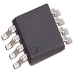
| 产品图片 |
|
| rohs | 符合RoHS无铅 / 符合限制有害物质指令(RoHS)规范要求 |
| 产品系列 | 电源管理 IC,线性稳压器,Analog Devices ADP3333ARMZ-2.5-R7anyCAP® |
| 数据手册 | |
| 产品型号 | ADP3333ARMZ-2.5-R7 |
| 产品种类 | |
| 供应商器件封装 | 8-MSOP |
| 其它名称 | ADP3333ARMZ-2.5-R7CT |
| 包装 | 剪切带 (CT) |
| 商标 | Analog Devices |
| 安装类型 | 表面贴装 |
| 安装风格 | SMD/SMT |
| 封装 | Reel |
| 封装/外壳 | 8-TSSOP,8-MSOP(0.118",3.00mm 宽) |
| 封装/箱体 | MSOP-8 |
| 工作温度 | -40°C ~ 85°C |
| 工厂包装数量 | 1000 |
| 最大输入电压 | 12 V |
| 最小输入电压 | 2.6 V |
| 标准包装 | 1 |
| 电压-跌落(典型值) | 0.14V @ 300mA |
| 电压-输入 | 最高 12V |
| 电压-输出 | 2.5V |
| 电流-输出 | 300mA |
| 电流-限制(最小值) | - |
| 稳压器拓扑 | 正,固定式 |
| 稳压器数 | 1 |
| 系列 | ADP3333 |
| 视频文件 | http://www.digikey.cn/classic/video.aspx?PlayerID=1364138032001&width=640&height=505&videoID=2245193149001 |
| 负载调节 | 0.04 mV |
| 输出电流 | 300 mA |


- 商务部:美国ITC正式对集成电路等产品启动337调查
- 曝三星4nm工艺存在良率问题 高通将骁龙8 Gen1或转产台积电
- 太阳诱电将投资9.5亿元在常州建新厂生产MLCC 预计2023年完工
- 英特尔发布欧洲新工厂建设计划 深化IDM 2.0 战略
- 台积电先进制程称霸业界 有大客户加持明年业绩稳了
- 达到5530亿美元!SIA预计今年全球半导体销售额将创下新高
- 英特尔拟将自动驾驶子公司Mobileye上市 估值或超500亿美元
- 三星加码芯片和SET,合并消费电子和移动部门,撤换高东真等 CEO
- 三星电子宣布重大人事变动 还合并消费电子和移动部门
- 海关总署:前11个月进口集成电路产品价值2.52万亿元 增长14.8%


.jpg)

PDF Datasheet 数据手册内容提取
High Accuracy Ultralow I , 300 mA, Q anyCAP Low Dropout Regulator ADP3333 FEATURES FUNCTIONAL BLOCK DIAGRAM High accuracy over line and load: ±0.8% @ 25°C, ±1.8% over temperature IN Q1 OUT Ultralow dropout voltage: 230 mV (maximum) @ 300 mA THERMAL ADP3333 R1 Requires only C = 1.0 µF for stability PROTECTION CC OUT anyCAP is stable with any type of capacitor (including MLCC) DRIVER gm Current and thermal limiting Low noise SD BAND GAP R2 Low shutdown current: < 1 µA REF 2−.460 V°C t oto 1 +28 V5 s°uCp apmlyb ireanntg tee mperature range GND 02615-001 Ultrasmall 8-lead MSOP package Figure 1. APPLICATIONS Cellular phones PCMCIA cards Personal digital assistants (PDAs) DSP/ASIC supplies GENERAL DESCRIPTION The ADP3333 is a member of the ADP333x family of precision ADP3333 low dropout (LDO) anyCAP® voltage regulators. Pin compatible NC 4 with the MAX8860, the ADP3333 operates with a wider input VIN 2 IN voltage range of 2.6 V to 12 V and delivers a load current up to OUT 1 VOUT 300 mA. ADP3333 stands out from other conventional LDOs 1CµIFN + +COUT 1µF with a novel architecture and an enhanced process that enables SD GND ipta ttoe notfefedr d peesrifgonr mreaqnuciree asd ovnalnyt aa g1e.s0 oμvFe ro uittsp cuotm cappeatcitiitoonr .f Iotrs OFFON 7 3 NC = NO CONNECT 02615-002 Figure 2. Typical Application Circuit stability. This device is insensitive to output capacitor equivalent series resistance (ESR) and is stable with any good quality capacitor, including ceramic (MLCC) types for space-restricted applications. The ADP3333 achieves exceptional accuracy of ±0.8% at room temperature and ±1.8% over temperature, line, and load variations. The dropout voltage of the ADP3333 is only 140 mV (typical) at 300 mA. This device also includes a safety current limit, thermal overload protection, and a shutdown feature. In shutdown mode, the ground current is reduced to less than 1 μA. The ADP3333 has ultralow quiescent current, 70 μA (typical) in light load situations. Rev. B Information furnished by Analog Devices is believed to be accurate and reliable. However, no responsibility is assumed by Analog Devices for its use, nor for any infringements of patents or other One Technology Way, P.O. Box 9106, Norwood, MA 02062-9106, U.S.A. rights of third parties that may result from its use. Specifications subject to change without notice. No license is granted by implication or otherwise under any patent or patent rights of Analog Devices. Tel: 781.329.4700 www.analog.com Trademarks and registered trademarks are the property of their respective owners. Fax: 781.461.3113 ©2001–2009 Analog Devices, Inc. All rights reserved.
ADP3333 TABLE OF CONTENTS Features .............................................................................................. 1 Theory of Operation .........................................................................9 Applications ....................................................................................... 1 Applications Information .............................................................. 10 Functional Block Diagram .............................................................. 1 Capacitor Selection .................................................................... 10 General Description ......................................................................... 1 Output Current Limit ................................................................ 10 Revision History ............................................................................... 2 Thermal Overload Protection .................................................. 10 Specifications ..................................................................................... 3 Calculating Junction Temperature ........................................... 10 Absolute Maximum Ratings ............................................................ 4 Shutdown Mode ......................................................................... 10 Thermal Resistance ...................................................................... 4 PCB Layout Considerations ...................................................... 10 ESD Caution .................................................................................. 4 Outline Dimensions ....................................................................... 11 Pin Configuration and Function Descriptions ............................. 5 Ordering Guide .......................................................................... 11 Typical Performance Characteristics ............................................. 6 REVISION HISTORY 4/09—Rev. A to Rev. B 8/03—Data Sheet Changed from Rev. 0 to Rev. A Changes to Voltage Accuracy, Line Regulation, Load Changes to Figure 1 ........................................................................... 1 Regulation, and Dropout Voltage Parameters, Table 1 ................ 3 Updated Output Capacitor Section.............................................. 10 Changes to Table 2 ............................................................................ 4 Updated Calculating Junction Temperature Section ................. 10 Added Thermal Resistance Section and Table 3; Renumbered Updated Outline Dimensions ....................................................... 11 Sequentially ....................................................................................... 4 Updated Ordering Guide .............................................................. 11 Changes to Table 4 ............................................................................ 5 Changes to Figure 5 and Figure 7 ................................................... 6 Changes to Figure 10, Figure 11, Figure 13, and Figure 15 ......... 7 Changes to Figure 16 and Figure 17 ............................................... 8 Changes to Output Capacitor Section and Calculating Junction Temperature Section ...................................................................... 10 Updated Outline Dimensions ....................................................... 11 Changes to Ordering Guide .......................................................... 11 Rev. B | Page 2 of 12
ADP3333 SPECIFICATIONS V = 6.0 V, C = C = 1.0 µF, T = −40°C to +125°C, unless otherwise noted. IN IN OUT J Table 1. Parameter1 Symbol Condition Min Typ Max Unit OUTPUT Voltage Accuracy2 V V = V + 0.3 V to 12 V, I = 0.1 mA to 300 mA, T = 25°C −0.8 +0.8 % OUT IN OUTNOM L J V = V + 0.3 V to 12 V, I = 0.1 mA to 300 mA −1.8 +1.8 % IN OUTNOM L Line Regulation2 ΔV /ΔV V = V + 0.3 V to 12 V, T = 25°C 0.04 mV/V IN OUT IN OUTNOM J Load Regulation ΔV /ΔI I = 0.1 mA to 300 mA, T = 25°C 0.04 mV/mA OUT OUT L J Dropout Voltage V V = 98% of V DROPOUT OUT OUTNOM I = 300 mA 140 230 mV L I = 200 mA 105 185 mV L I = 0.1 mA 30 mV L Peak Load Current I V = V + 1 V 600 mA LDPK IN OUTNOM Output Noise V f = 10 Hz to 100 kHz, C = 10 μF, I = 300 mA 45 μV rms NOISE L L GROUND CURRENT In Regulation I I = 300 mA 2.0 5.5 mA GND L I = 300 mA, T = 25°C 2.0 4.3 mA L J I = 300 mA, T = 85°C 1.5 3.3 mA L J I = 200 mA 1.4 mA L I = 10 mA 200 275 μA L I = 0.1 mA 70 100 μA L In Dropout I V = V − 100 mV, I = 0.1 mA 70 190 μA GND IN OUTNOM L V = V − 100 mV, I = 0.1 mA, T = 0°C to 125°C 70 160 μA IN OUTNOM L J In Shutdown I SD = 0 V, V = 12 V 0.01 1 μA GNDSD IN SHUTDOWN Threshold Voltage V Regulator on 2.0 V THSD Regulator off 0.4 V SD Input Current I 0 ≤ SD ≤ 12 V 0.85 7 μA SD 0 ≤ SD ≤ 5 V 0.8 4.5 μA Output Current in Shutdown I T = 25°C, V = 12 V 0.01 1 μA OSD J IN T = 125°C, V = 12 V 0.01 1 μA J IN 1 Application stable with no load. 2 V = 2.6 V for models with V ≤ 2.3 V. IN OUTNOM Rev. B | Page 3 of 12
ADP3333 ABSOLUTE MAXIMUM RATINGS Table 2. THERMAL RESISTANCE Parameter Rating Input Supply Voltage −0.3 V to +16 V θ is specified for the worst-case conditions, that is, a device JA Shutdown Input Voltage −0.3 V to +16 V soldered in a circuit board for surface-mount packages. Power Dissipation Internally Limited Table 3. Thermal Resistance Operating Ambient Temperature Range −40°C to +85°C Package Type θ Unit Operating Junction Temperature Range −40°C to +125°C JA 8-Lead MSOP (4-Layer) 158 °C/W Soldering Conditions JEDEC J-STD-020 8-Lead MSOP (2-Layer) 220 °C/W Stresses above those listed under Absolute Maximum Ratings ESD CAUTION may cause permanent damage to the device. This is a stress rating only; functional operation of the device at these or any other conditions above those indicated in the operational section of this specification is not implied. Exposure to absolute maximum rating conditions for extended periods may affect device reliability. Rev. B | Page 4 of 12
ADP3333 PIN CONFIGURATION AND FUNCTION DESCRIPTIONS OUT 1 8 NC ADP3333 IN 2 7 SD TOP VIEW GND 3 (Not to Scale) 6 NC NC1 4 5 NC NC = NO CONNECT 1CTOAN A BNEY COOTHNENRE CPTINE.D 02615-003 Figure 3. Pin Configuration Table 4. Pin Function Descriptions Pin No. Mnemonic Description 1 OUT Output of the Regulator. Bypass to ground with a 1.0 μF or larger capacitor. 2 IN Input Pin. Bypass to ground with a 1.0 μF or larger capacitor. 3 GND Ground Pin. 4 to 6, 8 NC No Connect. Best thermal performance is achieved when the NC pins are connected to the GND plane. 7 SD Active Low Shutdown Pin. Connect to ground to disable the regulator output. When shutdown is not used, connect this pin to the IN pin. Rev. B | Page 5 of 12
ADP3333 TYPICAL PERFORMANCE CHARACTERISTICS 2.502 2.5 VOUT = 2.5V VIN = 6V 0mA 2.500 2.0 GE (V) 2.498 100mA T (mA) LTA 2.496 REN 1.5 O R V U UT 2.494 D C TP 200mA UN 1.0 U O O 2.492 R G 300mA 0.5 2.490 2.488 02615-004 0 02615-007 3 4 5 6 7 8 9 10 11 12 0 50 100 150 200 250 300 INPUT VOLTAGE (V) OUTPUT CURRENT (mA) Figure 4. Line Regulation Output Voltage vs. Input Voltage Figure 7. Ground Current vs. Output Current 2.502 1.0 VVIONU =T 6=V 2.5V 0.9 0mA 2.500 0.8 0.7 200mA GE (V) 2.498 E (%) 00..56 TA 2.496 NG 0.4 L A VO CH 0.3 UT 2.494 UT 0.2 TP TP 0.1 300mA U U O 2.492 O 0 –0.1 22..449808 02615-005 –––000...234 0mA 02615-008 0 50 100 150 200 250 300 –50 –25 0 25 50 75 100 125 OUTPUT CURRENT (mA) JUNCTION TEMPERATURE (°C) Figure 5. Output Voltage vs. Output Current Figure 8. Output Voltage Variation % vs. Junction Temperature 140 3.5 IL = 100µA VOUT = 2.5V VIN = 6V 120 3.0 GROUND CURRENT (µA) 104860000 IL = 0µA GROUND CURRENT (mA) 1122....0505 IL = 300ILm =A 200mILA = 100mA 200 02615-006 0.50 IL = 0mA 02615-009 0 2 4 6 8 10 12 –50 –25 0 25 50 75 100 125 INPUT VOLTAGE (V) JUNCTION TEMPERATURE (°C) Figure 6. Ground Current vs. Input Voltage Figure 9. Ground Current vs. Junction Temperature Rev. B | Page 6 of 12
ADP3333 0.16 VOUT = 2.5V 0.14 2.52 RCLL == 81.µ3FΩ V) GE (m 0.12 (V)UT 2.51 TA 0.10 VO 2.50 L O V T 0.08 2.49 U P T U 0.06 O T/ U NP 0.04 V) 3.50 I (N 0.020 02615-010 VI 3.00 02615-013 0 50 100 150 200 250 300 40 80 140 180 OUTPUT CURRENT (mA) TIME (µs) Figure 10. Dropout Voltage vs. Output Current Figure 13. Line Transient Response, C = 1 µF L VOUT = 2.5V VOUT = 2.5V 3.0 SRDL == 8V.I3NΩ 2.52 RCLL == 81.03µΩF OLTAGE (V) 22..50 VIN V (V)OUT 22..5501 V UT 1.5 2.49 P T U O 1.0 UT/ VOUT INP 0.5 (V)N 3.50 0 02615-011 VI 3.00 02615-014 1 2 3 4 40 80 140 180 TIME (Seconds) TIME (µs) Figure 11. V During Power-Up/Power-Down Figure 14. Line Transient Response, C = 10 µF OUT L 3 COUT = 1µF V) 2.7 CVVIOLN U ==T 1 4=µV F2.5V (V)UT 2 V (OUT 2.6 O V 1 2.5 COUT = 10µF 0 2.4 V (V)IN 42 (mA)UT 300 O 0 VSRODL U ==T 8 V=.I3 N2Ω.5V 02615-012 I 10 02615-015 200 400 600 800 200 400 600 800 TIME (µs) TIME (µs) Figure 12. Power-Up Response Figure 15. Load Transient Response, C = 1 µF L Rev. B | Page 7 of 12
ADP3333 –20 V (V)OUT 22..76 VCVIOLN U ==T 1 4=0V µ2F.5V N (dB) ––3400 VOUT = 2.2V CILL = = 5 10µ0FmA CILL = = 5 1000µmFA 2.5 ECTIO –50 CILL = = 5 10µµFA 2.4 EJ R –60 E L P mA) 300 RIP –70 I (OUT 10 02615-016 ––890010 100 1k 10k 100kCILL = = 5 100µµA1FM 10M02615-019 200 400 600 800 TIME (µs) FREQUENCY (Hz) Figure 19. Power Supply Ripple Rejection Figure 16. Load Transient Response, C = 10 µF L 120 100 V) ( UT 2.5 VO V) 80 µ 0 E ( S OI 60 3 N MS 300mA 2 VIN = 6V R 40 A) 0mA (UT 1 O 20 I 0 VIN = 3.6V 02615-017 00 10 20 30 40 5002615-020 200 400 600 800 CL (µF) TIME (µs) Figure 20. RMS Noise vs. C (10 Hz to 100 kHz) Figure 17. Short-Circuit Current L 100 VOUT = 2.5V IL = 1mA 3 1µF L 10 A VOUT 12 10µF E SPECTRµV/Hz) 1 CL = 10µF CL = 1µF 0 10µF 1µF VIN = 6V AGE NOISDENSITY ( 0.1 VOUT = 2.5V LT 2 RL = 8.3Ω VO 0.01 DD SS V 0 02615-018 0.00110 100 1k 10k 100k 1M02615-021 200 400 600 800 FREQUENCY (Hz) TIME (µs) Figure 21. Output Noise Density Figure 18. Turn-On/Turn-Off Response Rev. B | Page 8 of 12
ADP3333 THEORY OF OPERATION The ADP3333 anyCAP LDO uses a single control loop for temperature stable output. This unique arrangement specifically regulation and reference functions (see Figure 22). The output corrects for the loading of the divider so that the error resulting voltage is sensed by a resistive voltage divider consisting of R1 from base current loading in conventional circuits is avoided. and R2 that is varied to provide the available output voltage The patented amplifier controls a new and unique noninverting option. Feedback is taken from this network by way of a series driver that drives the pass transistor, Q1. The use of this special diode (D1) and a second resistor divider (R3 and R4) to the noninverting driver enables the frequency compensation to input of an amplifier. include the load capacitor in a pole splitting arrangement to INPUT OUTPUT achieve reduced sensitivity to the value, type, and ESR of the ATTENUATION load capacitance. Q1 COMPENSATION (VBAND GAP/VOUT) R1 NOWNIIDNEVBEARNTDING CAPAgmCITORPVTOAST R3 D1 FB (a) CL Mvaoluset sL fDorO tsh pe loaucetp vuetr cya sptraiccitt orre qbueicraeumsee nthtse oy na rteh ed irfafincguel to tfo E SR DRIVER R4 PCTUARTRENT RL stabilize due to the uncertainty of load capacitance and resistance. R2 Moreover, the ESR value required to keep conventional LDOs ADP3333 stable changes depending on load and temperature. These ESR GND 02615-022 loifm thiteaitrio unnsc mleaark es pdeecsiifgicnaitnigo nwsi tahn dL DexOtrse mmoe rvea driiafftiicounlst obveecra use Figure 22. Functional Block Diagram temperature. A very high gain error amplifier is used to control this loop. With the ADP3333 anyCAP LDO, this is no longer true. This The amplifier is constructed in such a way that at equilibrium it device can be used with virtually any good quality capacitor, produces a large, temperature-proportional input offset voltage with no constraint on the minimum ESR. Its innovative design that is repeatable and very well controlled. The temperature allows the circuit to be stable with just a small 1.0 μF capacitor proportional offset voltage is combined with the complementary on the output. Additional advantages of the pole splitting diode voltage to form a virtual band gap voltage, implicit in the scheme include superior line noise rejection and very high network, although it never appears explicitly in the circuit. regulator gain, which leads to excellent line and load regulation. Ultimately, this patented design makes it possible to control the An impressive ±1.8% accuracy is guaranteed over line, load, and loop with only one amplifier. This technique also improves the temperature. noise characteristics of the amplifier by providing more flexibility Additional features of the circuit include current limit and on the trade-off of noise sources and leads to a low noise design. thermal shutdown. The R1, R2 divider is chosen in the same ratio as the band gap voltage to the output voltage. Although the R1/R2 resistor divider is loaded by the diode, D1, and a second divider consisting of R3 and R4, the values can be chosen to produce a Rev. B | Page 9 of 12
ADP3333 APPLICATIONS INFORMATION CAPACITOR SELECTION CALCULATING JUNCTION TEMPERATURE Output Capacitor Device power dissipation is calculated as follows: The stability and transient response of the LDO is a function of P = (V − V ) I + (V ) I D IN OUT L IN GND the output capacitor. The ADP3333 is stable with a wide range where I and I are the load current and ground current, and of capacitor values, types, and ESR (anyCAP). A capacitor as L GND V and V are the input and output voltages, respectively. low as 1.0 μF is all that is needed for stability. Larger capacitors IN OUT can be used if high current surges on the output are anticipated. Assuming the worst-case operating conditions are IL = 300 mA, The ADP3333 is stable with extremely low ESR capacitors (ESR IGND = 2.0 mA, VIN = 4.0 V, and VOUT = 3.0 V, the device power ≈ 0), such as multilayer ceramic capacitors (MLCC) or OSCON. dissipation is Note that the effective capacitance of some capacitor types falls P = (4.0 V − 3.0 V) 300 mA + (4.0 V) 2.0 mA = 308 mW D below the minimum rated value over temperature or with dc The package used on the ADP3333 has a thermal resistance of voltage. Ensure that the capacitor provides at least 1.0 μF of 158°C/W for 4-layer boards. The junction temperature rise capacitance over temperature and dc bias. above ambient is approximately equal to Input Bypass Capacitor T = 0.308 W × 158°C/W = 48.7°C JA An input bypass capacitor is not strictly required but is recom- Therefore, to limit the junction temperature to 125°C, the mended in any application involving long input wires or high maximum allowable ambient temperature is source impedance. Connecting a 1.0 μF capacitor from the input to ground reduces the circuit’s sensitivity to printed circuit board TA(MAX) = 125°C − 48.7°C = 76.3°C (PCB) layout and input transients. If a larger output capacitor is SHUTDOWN MODE necessary, then a larger value input capacitor is also recommended. Applying a high signal to the shutdown pin, SD, or connecting OUTPUT CURRENT LIMIT it to the input pin, IN, turns the output on. Pulling the shutdown The ADP3333 is short-circuit protected by limiting the pass pin to 0.3 V or below, or connecting it to ground, turns the transistor’s base drive current. The maximum output current is output off. In shutdown mode, the quiescent current is reduced limited to about 1 A (see Figure 17). to less than 1 μA. THERMAL OVERLOAD PROTECTION PCB LAYOUT CONSIDERATIONS The ADP3333 is protected against damage due to excessive power Use the following general guidelines when designing printed dissipation by its thermal overload protection circuit. Thermal circuit boards: protection limits the die temperature to a maximum of 165°C. Keep the output capacitor as close as possible to the output Under extreme conditions (that is, high ambient temperature and and ground pins. power dissipation) where the die temperature starts to rise above Keep the input capacitor as close as possible to the input 165°C, the output current is reduced until the die temperature and ground pins. drops to a safe level. PCB traces with larger cross sectional areas remove more Current and thermal limit protections are intended to protect heat from the ADP3333. For optimum heat transfer, use the device against accidental overload conditions. For normal thick copper with wide traces. operation, the device’s power dissipation should be externally Connect the NC pins (Pin 4, Pin 5, Pin 6, and Pin 8) to limited so that the junction temperature does not exceed 125°C. ground for better thermal performance. The thermal resistance can be decreased by approximately 10% by adding a few square centimeters of copper area to the lands connected to the pins of the LDO. Use additional copper layers or planes to reduce the thermal resistance. Again, connecting the other layers to the GND and NC pins of the ADP3333 is best, but not necessary. When connecting the ground pad to other layers, use multiple vias. Rev. B | Page 10 of 12
ADP3333 OUTLINE DIMENSIONS 3.20 3.00 2.80 8 5 5.15 3.20 4.90 3.00 4.65 2.80 1 4 PIN 1 0.65 BSC 0.95 0.85 1.10 MAX 0.75 0.80 0.15 0.38 0.23 8° 0.60 0.00 0.22 0.08 0° 0.40 COPLANARITY SEATING 0.10 PLANE COMPLIANT TO JEDEC STANDARDS MO-187-AA Figure 23. 8-Lead Mini Small Outline Package [MSOP] (RM-8) Dimensions shown in millimeters ORDERING GUIDE Model Temperature Range Output Voltage (V) Package Description Package Option Branding ADP3333ARM-1.5-RL −40°C to +85°C 1.5 8-Lead MSOP RM-8 LKA ADP3333ARM-1.5-RL7 −40°C to +85°C 1.5 8-Lead MSOP RM-8 LKA ADP3333ARM-1.8-RL −40°C to +85°C 1.8 8-Lead MSOP RM-8 LKB ADP3333ARM-1.8-RL7 −40°C to +85°C 1.8 8-Lead MSOP RM-8 LKB ADP3333ARM-2.5-RL −40°C to +85°C 2.5 8-Lead MSOP RM-8 LKC ADP3333ARM-2.5-RL7 −40°C to +85°C 2.5 8-Lead MSOP RM-8 LKC ADP3333ARM-2.77-RL −40°C to +85°C 2.77 8-Lead MSOP RM-8 LKD ADP3333ARM-2.77-R7 −40°C to +85°C 2.77 8-Lead MSOP RM-8 LKD ADP3333ARM-3-REEL −40°C to +85°C 3 8-Lead MSOP RM-8 LKE ADP3333ARM-3-REEL7 −40°C to +85°C 3 8-Lead MSOP RM-8 LKE ADP3333ARM-3.15-RL −40°C to +85°C 3.15 8-Lead MSOP RM-8 LKF ADP3333ARM-3.15-R7 −40°C to +85°C 3.15 8-Lead MSOP RM-8 LKF ADP3333ARM-3.3-RL −40°C to +85°C 3.3 8-Lead MSOP RM-8 LKG ADP3333ARM-3.3-RL7 −40°C to +85°C 3.3 8-Lead MSOP RM-8 LKG ADP3333ARM-5-REEL −40°C to +85°C 5 8-Lead MSOP RM-8 LKH ADP3333ARM-5-REEL7 −40°C to +85°C 5 8-Lead MSOP RM-8 LKH ADP3333ARMZ-1.5-R71 −40°C to +85°C 1.5 8-Lead MSOP RM-8 L1X ADP3333ARMZ-1.5-RL1 −40°C to +85°C 1.5 8-Lead MSOP RM-8 L1X ADP3333ARMZ-1.8-RL1 −40°C to +85°C 1.8 8-Lead MSOP RM-8 L1U ADP3333ARMZ-1.8RL71 −40°C to +85°C 1.8 8-Lead MSOP RM-8 L1U ADP3333ARMZ-2.5-RL1 −40°C to +85°C 2.5 8-Lead MSOP RM-8 L1V ADP3333ARMZ-2.5-R71 −40°C to +85°C 2.5 8-Lead MSOP RM-8 L1V ADP3333ARMZ-2.77R71 −40°C to +85°C 2.77 8-Lead MSOP RM-8 L1Y ADP3333ARMZ-3-R71 −40°C to +85°C 3.0 8-Lead MSOP RM-8 L1W ADP3333ARMZ-3.15R71 −40°C to +85°C 3.15 8-Lead MSOP RM-8 L1Z ADP3333ARMZ-3.3-R71 −40°C to +85°C 3.3 8-Lead MSOP RM-8 L20 ADP3333ARMZ-3.3-RL1 −40°C to +85°C 3.3 8-Lead MSOP RM-8 L20 ADP3333ARMZ-5-R71 −40°C to +85°C 5.0 8-Lead MSOP RM-8 L21 ADP3333ARMZ-5-RL1 −40°C to +85°C 5.0 8-Lead MSOP RM-8 L21 1 Z = RoHS Compliant Part. Rev. B | Page 11 of 12
ADP3333 NOTES ©2001–2009 Analog Devices, Inc. All rights reserved. Trademarks and registered trademarks are the property of their respective owners. D02615-0-4/09(B) Rev. B | Page 12 of 12