ICGOO在线商城 > 集成电路(IC) > PMIC - 稳压器 - 线性 > ADP1720ARMZ-5-R7
 Datasheet下载
- 型号: ADP1720ARMZ-5-R7
- 制造商: Analog
- 库位|库存: xxxx|xxxx
- 要求:
| 数量阶梯 | 香港交货 | 国内含税 |
| +xxxx | $xxxx | ¥xxxx |
查看当月历史价格
查看今年历史价格
ADP1720ARMZ-5-R7产品简介:
ICGOO电子元器件商城为您提供ADP1720ARMZ-5-R7由Analog设计生产,在icgoo商城现货销售,并且可以通过原厂、代理商等渠道进行代购。 ADP1720ARMZ-5-R7价格参考。AnalogADP1720ARMZ-5-R7封装/规格:PMIC - 稳压器 - 线性, Linear Voltage Regulator IC Positive Fixed 1 Output 5V 50mA 8-MSOP。您可以下载ADP1720ARMZ-5-R7参考资料、Datasheet数据手册功能说明书,资料中有ADP1720ARMZ-5-R7 详细功能的应用电路图电压和使用方法及教程。
ADP1720ARMZ-5-R7 是由 Analog Devices Inc.(ADI)生产的一款线性稳压器(PMIC - Power Management IC),属于低 dropout (LDO) 稳压器系列。以下是其主要应用场景及特点:

 1. 便携式设备
   - ADP1720ARMZ-5-R7 的低静态电流和高效率特性使其非常适合用于电池供电的便携式设备,例如:
     - 手持式医疗设备(如血糖仪、脉搏血氧仪)
     - 消费类电子产品(如智能手机、平板电脑、电子书阅读器)
     - 可穿戴设备(如智能手表、健身追踪器)

 2. 通信设备
   - 在通信领域中,该稳压器可用于为以下设备提供稳定的电源:
     - 无线传感器节点
     - 蓝牙模块
     - Wi-Fi 模块
   - 其低噪声输出有助于提高射频电路的性能。

 3. 工业自动化
   - ADP1720ARMZ-5-R7 的高可靠性使其适用于工业环境中的各种应用,例如:
     - 工业控制器
     - 数据采集系统
     - 远程监控设备
   - 它能够为微控制器、传感器和其他低功耗组件提供稳定电源。

 4. 汽车电子
   - 在汽车电子领域,这款 LDO 稳压器可以为以下系统供电:
     - 车载信息娱乐系统
     - 仪表盘模块
     - 传感器接口
   - 其宽输入电压范围和良好的瞬态响应能力适合汽车电气环境。

 5. 消费类音频设备
   - ADP1720ARMZ-5-R7 的低噪声特性使其成为音频设备的理想选择,例如:
     - 便携式音响
     - 耳机放大器
     - 音频解码器
   - 它能有效减少电源噪声对音质的影响。

 6. 物联网 (IoT) 设备
   - 对于需要长时间运行且功耗敏感的 IoT 设备,这款 LDO 稳压器非常适用,例如:
     - 智能家居设备(如温控器、烟雾报警器)
     - 环境监测传感器
     - 智能锁

 特点总结:
- 输出电压:固定为 5V。
- 输入电压范围:2.3V 至 20V。
- 最大输出电流:200mA。
- 低 dropout 电压(典型值为 300mV)。
- 低静态电流(典型值为 25μA)。
- 高纹波抑制比(PSRR),适合对噪声敏感的应用。
- 小型封装(SOT-23),节省空间。

综上所述,ADP1720ARMZ-5-R7 广泛应用于需要高效、低噪声和小尺寸电源解决方案的各种场景中。
| 参数 | 数值 |
| 产品目录 | 集成电路 (IC)半导体 |
| 描述 | IC REG LDO 5V 50MA 8MSOP线性稳压器 50mA Hi VTG Micropwr |
| 产品分类 | |
| 品牌 | Analog Devices Inc |
| 产品手册 | |
| 产品图片 |
|
| rohs | 符合RoHS无铅 / 符合限制有害物质指令(RoHS)规范要求 |
| 产品系列 | 电源管理 IC,线性稳压器,Analog Devices ADP1720ARMZ-5-R7- |
| 数据手册 | |
| 产品型号 | ADP1720ARMZ-5-R7 |
| 产品培训模块 | http://www.digikey.cn/PTM/IndividualPTM.page?site=cn&lang=zhs&ptm=19143 |
| 产品目录页面 | |
| 产品种类 | 线性稳压器 |
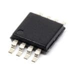
| 供应商器件封装 | 8-MSOP |
| 其它名称 | ADP1720ARMZ-5-R7TR |
| 包装 | 带卷 (TR) |
| 商标 | Analog Devices |
| 安装类型 | 表面贴装 |
| 安装风格 | SMD/SMT |
| 封装 | Reel |
| 封装/外壳 | 8-TSSOP,8-MSOP(0.118",3.00mm 宽) |
| 封装/箱体 | MSOP-8 |
| 工作温度 | -40°C ~ 125°C |
| 工厂包装数量 | 1000 |
| 最大工作温度 | + 125 C |
| 最大输入电压 | 28 V |
| 最小工作温度 | - 40 C |
| 最小输入电压 | 4 V |
| 标准包装 | 1,000 |
| 电压-跌落(典型值) | 0.275V @ 50mA |
| 电压-输入 | 最高 28V |
| 电压-输出 | 5V |
| 电流-输出 | 50mA |
| 电流-限制(最小值) | 55mA |
| 稳压器拓扑 | 正,固定式 |
| 稳压器数 | 1 |
| 系列 | ADP1720 |
| 视频文件 | http://www.digikey.cn/classic/video.aspx?PlayerID=1364138032001&width=640&height=505&videoID=2245193149001 |
| 设计资源 | |
| 输出电流 | 50 mA |
| 配用 | /product-detail/zh/ADP1720-3.3-EVALZ/ADP1720-3.3-EVALZ-ND/1680439/product-detail/zh/ADP1720-EVALZ/ADP1720-EVALZ-ND/1680440/product-detail/zh/ADP1720-5-EVALZ/ADP1720-5-EVALZ-ND/1805676 |


PDF Datasheet 数据手册内容提取
50 mA, High Voltage, Micropower Linear Regulator ADP1720 FEATURES TYPICAL APPLICATION CIRCUITS Wide input voltage range: 4 V to 28 V ADP1720 FIXED Maximum output current: 50 mA Low light load current: 1 GND GND 8 28 μA at 0 μA load VIN = 28V 2 IN GND 7 1µF 3 OUT GND 6 35 μA at 100 μA load 4 EN GND 5 LLooww dshrouptdoouwt vno clutarrgeen: t2: 705.7 m μVA @ 50 mA load VOUT = 5V 1µF 06111-001 Initial accuracy: ±0.5% Figure 1. ADP1720 with Fixed Output Voltage, 5.0 V Accuracy over line, load, and temperature: ±2% Stable with small 1μF ceramic output capacitor ADP1720 R2 ADJUSTABLE Fixed 3.3 V and 5.0 V output voltage options Adjustable output voltage option: 1.225 V to 5.0 V R1 1 ADJ GND 8 Current limit and thermal overload protection VIN = 12V 2 IN GND 7 1µF 3 OUT GND 6 Logic controlled enable SApPaPceL-IsCaAviTnIgO thNeSrm ally enhanced MSOP package 1.225V(1 +V RO1U/RT 2=) 1µF 4 EN GND 5 06111-002 Figure 2. ADP1720 with Adjustable Output Voltage, 1.225 V to 5.0 V DC-to-DC post regulation PCMCIA regulation Keep-alive power in portable equipment Industrial applications GENERAL DESCRIPTION The ADP1720 is a high voltage, micropower, low dropout linear The ADP1720 is optimized for stable operation with small 1 μF regulator. Operating over a very wide input voltage range of 4 V ceramic output capacitors, allowing for good transient perform- to 28 V, the ADP1720 can provide up to 50 mA of output current. ance while occupying minimal board space. With just 28 μA of quiescent supply current and a micropower The ADP1720 operates from –40°C to +125°C and uses current shutdown mode, this device is ideal for applications that require limit protection and thermal overload protection circuits to low quiescent current. prevent damage to the device in adverse conditions. The ADP1720 is available in fixed output voltages of 3.3 V and Available in a small thermally enhanced MSOP package, the 5.0 V. An adjustable version is also available, which allows the ADP1720 provides a compact solution with low thermal resistance. output to be set anywhere between 1.225 V and 5.0 V. An enable function that allows external circuits to turn on and turn off the ADP1720 output is available. For automatic startup, the enable (EN) pin can be connected directly to the input rail. Rev. A Information furnished by Analog Devices is believed to be accurate and reliable. However, no responsibility is assumed by Analog Devices for its use, nor for any infringements of patents or other One Technology Way, P.O. Box 9106, Norwood, MA 02062-9106, U.S.A. rights of third parties that may result from its use. Specifications subject to change without notice. No license is granted by implication or otherwise under any patent or patent rights of Analog Devices. Tel: 781.329.4700 www.analog.com Trademarks and registered trademarks are the property of their respective owners. Fax: 781.461.3113 ©2007 Analog Devices, Inc. All rights reserved.
ADP1720 TABLE OF CONTENTS Features .............................................................................................. 1 Typical Performance Characteristics ..............................................7 Applications ....................................................................................... 1 Theory of Operation ...................................................................... 10 Typical Application Circuits ............................................................ 1 Adjustable Output Voltage (ADP1720 Adjustable) ............... 10 General Description ......................................................................... 1 Applications Information .............................................................. 11 Revision History ............................................................................... 2 Capacitor Selection .................................................................... 11 Specifications ..................................................................................... 3 Current Limit and Thermal Overload Protection ................. 11 Absolute Maximum Ratings ............................................................ 5 Thermal Considerations ............................................................ 12 Thermal Resistance ...................................................................... 5 Printed Circuit Board Layout Considerations ....................... 14 ESD Caution .................................................................................. 5 Outline Dimensions ....................................................................... 15 Pin Configurations and Function Descriptions ........................... 6 Ordering Guide .......................................................................... 15 REVISION HISTORY 7/07—Rev. 0 to Rev. A Change to Figure 1 ........................................................................... 1 Changes to Table 1 ............................................................................ 3 Changes to Ordering Guide .......................................................... 15 2/07—Revision 0: Initial Version Rev. A | Page 2 of 16
ADP1720 SPECIFICATIONS V = 12 V, I = 100 μA, C = C = 1 μF, T = 25°C, unless otherwise noted. IN OUT IN OUT A Table 1. Parameter Symbol Conditions Min Typ Max Unit INPUT VOLTAGE RANGE V T = –40°C to +125°C 4 28 V IN J OPERATING SUPPLY CURRENT I I = 0 μA 28 μA GND OUT I = 0 μA, V = V + 0.5 Vor 4V(whichever is 80 μA OUT IN OUT greater), T = –40°C to +125°C J I = 100 μA 35 μA OUT I = 100 μA, V = V + 0.5 V or 4 V (whichever is 120 μA OUT IN OUT greater), T = –40°C to +125°C J I = 1 mA 74 μA OUT I = 1 mA, V = V + 0.5 V or 4 V (whichever is 340 μA OUT IN OUT greater), T = –40°C to +125°C J I = 10 mA 300 μA OUT I = 10 mA, V = V + 0.5 V or 4 V (whichever is 900 μA OUT IN OUT greater), T = –40°C to +125°C J 100 μA < I < 50 mA, V = V + 0.5 V or 4 V 1185 2115 μA OUT IN OUT (whichever is greater), T = –40°C to +125°C J SHUTDOWN CURRENT I EN = GND 0.7 μA GND-SD EN = GND, T = –40°C to +125°C 1.5 μA J OUTPUT Fixed Output V I = 100 μA –0.5 +0.5 % OUT OUT Voltage Accuracy 100 μA < I < 50 mA –1 +1 % OUT 100 μA < I < 50 mA, T = –40°C to +125°C –2 +2 % OUT J Adjustable Output1 V I = 100 μA 1.2188 1.2250 1.2311 V OUT OUT Voltage Accuracy 100 μA < I < 50 mA 1.2127 1.2372 V OUT 100 μA < I < 50 mA, T = –40°C to +125°C 1.2005 1.2495 V OUT J Noise (10 Hz to 100 kHz) OUT V = 1.6 V, C = 1 μF 146 μV rms NOISE OUT OUT V = 1.6 V, C = 10 μF 124 μV rms OUT OUT VOUT = 5 V, COUT = 1 μF 340 μV rms VOUT = 5 V, COUT = 10 μF 266 μV rms REGULATION Line Regulation ∆V /∆V V = (V + 0.5 V) to 28 V, T = –40°C to +125°C –0.02 +0.02 %/V OUT IN IN OUT J Load Regulation2 ∆V /∆I 1 mA < I < 50 mA 0.001 %/mA OUT OUT OUT 1 mA < I < 50 mA, T = –40°C to +125°C 0.005 %/mA OUT J DROPOUT VOLTAGE3 V I = 10 mA 55 mV DROPOUT OUT I = 10 mA, T = –40°C to +125°C 105 mV OUT J I = 50 mA 275 mV OUT I = 50 mA, T = –40°C to +125°C 480 mV OUT J START-UP TIME4 T 200 μs START-UP CURRENT LIMIT THRESHOLD5 I 55 90 140 mA LIMIT THERMAL CHARACTERISTICS Thermal Shutdown TSSD T J rising 150 °C Threshold Thermal Shutdown TSSD-HYS 15 °C Hysteresis EN CHARACTERISTICS EN Input Logic High V 4 V ≤ V ≤ 28 V 1.8 V IH IN Logic Low V 4 V ≤ V ≤ 28 V 0.4 V IL IN Leakage Current V EN = GND 0.1 1 μA I-LEAKAGE EN = IN 0.5 1 μA ADJ INPUT BIAS CURRENT ADJ 30 100 nA I-BIAS (ADP1720 ADJUSTABLE) Rev. A | Page 3 of 16
ADP1720 Parameter Symbol Conditions Min Typ Max Unit POWER SUPPLY REJECTION RATIO PSRR f = 120 Hz, V = 8 V, V = 1.6 V –90 dB IN OUT f = 1 kHz, V = 8 V, V = 1.6 V –80 dB IN OUT f = 10 kHz, V = 8 V, V = 1.6 V –60 dB IN OUT f = 120 Hz, V = 8 V, V = 5 V –83 dB IN OUT f = 1 kHz, V = 8 V, V = 5 V –70 dB IN OUT f = 10 kHz, V = 8 V, V = 5 V –50 dB IN OUT 1 Accuracy when OUT is connected directly to ADJ. When OUT voltage is set by external feedback resistors, absolute accuracy in adjust mode depends on the tolerances of resistors used. 2 Based on an end-point calculation using 1 mA and 50 mA loads. See Figure 6 for typical load regulation performance for loads less than 1 mA. 3 Dropout voltage is defined as the input to output voltage differential when the input voltage is set to the nominal output voltage. This applies only for output voltages above 4 V. 4 Start-up time is defined as the time between the rising edge of EN to OUT being at 95% of its nominal value. 5 Current limit threshold is defined as the current at which the output voltage drops to 90% of the specified typical value. For example, the current limit for a 5.0 V output voltage is defined as the current that causes the output voltage to drop to 90% of 5.0 V, or 4.5 V. Rev. A | Page 4 of 16
ADP1720 ABSOLUTE MAXIMUM RATINGS Table 2. THERMAL RESISTANCE Parameter Rating θ is specified for the worst-case conditions, that is, a device JA IN to GND –0.3 V to +30 V soldered in a circuit board for surface-mount packages. OUT to GND –0.3 V to IN or +6 V (whichever is less) Table 3. Thermal Resistance EN to GND –0.3 V to +30 V Package Type θ θ Unit JA JC ADJ to GND –0.3 V to +6 V 8-Lead MSOP 118 57 °C/W Storage Temperature Range –65°C to +150°C Operating Junction –40°C to +125°C Temperature Range ESD CAUTION Soldering Conditions JEDEC J-STD-020 Stresses above those listed under Absolute Maximum Ratings may cause permanent damage to the device. This is a stress rating only; functional operation of the device at these or any other conditions above those indicated in the operational section of this specification is not implied. Exposure to absolute maximum rating conditions for extended periods may affect device reliability. Rev. A | Page 5 of 16
ADP1720 PIN CONFIGURATIONS AND FUNCTION DESCRIPTIONS GND 1 8 GND ADJ 1 8 GND ADP1720 ADP1720 IN 2 FIXED 7 GND IN 2 ADJUSTABLE 7 GND OEUNT 34 (NToOt Pto V SIEcaWle) 65 GGNNDD 06111-003 OEUNT 34 (NToOt Pto V SIEcaWle) 65 GGNNDD 06111-004 Figure 3. 8-Lead MSOP Figure 4. 8-Lead MSOP Table 4. Pin Function Descriptions ADP1720 ADP1720 Fixed Adjustable Pin No. Pin No. Mnemonic Description 1 N/A GND This pin is internally connected to ground. N/A 1 ADJ Adjust. A resistor divider from OUT to ADJ sets the output voltage. 2 2 IN Regulator Input Supply. Bypass IN to GND with a 1 μF or greater capacitor. 3 3 OUT Regulated Output Voltage. Bypass OUT to GND with a 1 μF or greater capacitor. 4 4 EN Enable Input. Drive EN high to turn on the regulator; drive it low to turn off the regulator. For automatic startup, connect EN to IN. 5 5 GND Ground. 6 6 GND Ground. 7 7 GND Ground. 8 8 GND Ground. Rev. A | Page 6 of 16
ADP1720 TYPICAL PERFORMANCE CHARACTERISTICS V = 12 V, V = 5 V, I = 100 μA, C = C = 1 μF, T = 25°C, unless otherwise noted. IN OUT OUT IN OUT A 5.03 1200 5.02 1000 5.01 ILOAD = 50mA ILOAD = 1mA 800 ILOAD = 25mA ILOAD = 100µA ILOAD = 10mA ILOAD = 10µA V) 5.00 A) (UT (µD 600 O N V 4.99 G I 400 4.98 ILOAD = 10µA ILOAD = 100µA ILOAD = 1mA 4.97 ILOAD = 10mA 200 4.96 IILLOOAADD == 2550mmAA 06111-005 0 06111-008 –40 –5 25 85 125 –40 –5 25 85 125 TJ (°C) TJ (°C) Figure 5. Output Voltage vs. Junction Temperature Figure 8. Ground Current vs. Junction Temperature 5.0015 1200 5.0010 1000 5.0005 5.0000 800 4.9995 V) A) (UT4.9990 (µD 600 O N V G 4.9985 I 400 4.9980 4.9975 200 44..99996750 06111-006 0 06111-009 0.01 0.1 1 10 100 0.01 0.1 1 10 100 ILOAD (mA) ILOAD (mA) Figure 6. Output Voltage vs. Load Current Figure 9. Ground Current vs. Load Current 5.010 1400 ILOAD = 10µA ILOAD = 50mA ILOAD = 1mA 5.008 ILOAD = 100µA ILOAD = 25mA ILOAD = 100µA ILOAD = 1mA 1200 ILOAD = 10mA ILOAD = 10µA 5.006 ILOAD = 10mA ILOAD = 25mA 5.004 ILOAD = 50mA 1000 5.002 V) A) 800 (UT5.000 (µD O N V G 600 4.998 I 4.996 400 4.994 200 44..999902 06111-007 0 06111-010 0 5 10 15 20 25 30 0 5 10 15 20 25 30 VIN (V) VIN (V) Figure 7. Output Voltage vs. Input Voltage Figure 10. Ground Current vs. Input Voltage Rev. A | Page 7 of 16
ADP1720 300 3.5 3.0 250 ILOAD = 50mA 2.5 200 V) (mDROPOUT 150 I (mA)GND 21..05 I2L5OmAAD = V 100 1.0 I1L0OmAAD = 500 06111-011 0.05 I1LmOAAD = 06111-013 1 10 100 4.9 5.0 5.1 5.2 5.3 5.4 ILOAD (mA) VIN (V) Figure 11. Dropout Voltage vs. Load Current Figure 13. Ground Current vs. Input Voltage (in Dropout) 5.05 0 ILOAD = 1mA VIN = 8V 5.00 –10 VOUT = 1.6V COUT = 1µF 4.95 –20 VRIPPLE = 50mV 4.90 –30 1mA V) 4.85 ILOAD = 50mA B) –40 10mA (UT ILOAD = 25mA R (d –50 VO 4.80 SR ILOAD = 10mA P –60 100µA 4.75 –70 4.70 –80 44..6605 06111-012 –1–0900 06111-014 4.9 5.0 5.1 5.2 5.3 5.4 10 100 1k 10k 100k 1M 10M VIN (V) FREQUENCY (Hz) Figure 12. Output Voltage vs. Input Voltage (in Dropout) Figure 14. Power Supply Rejection Ratio vs. Frequency (1.6 V Adjustable Output) Rev. A | Page 8 of 16
ADP1720 0 VIN = 8V –10 VOUT = 5V COUT = 1µF –20 VRIPPLE = 50mV VIN STEP FROM 6V TO 7V –30 VOUT = 5V PSRR (dB) –––456000 1mA 10mA V/DIV 1 CICLIOONUA =TD 1==µ 15Fµ0FmA 100µA 2 –70 V VOUT –80 V/DI 2 m –1–090010 100 1k 10k 100k 1M 10M06111-015 10 06111-017 FREQUENCY (Hz) TIME (100µs/DIV) Figure 15. Power Supply Rejection Ratio vs. Frequency Figure 17. Line Transient Response (5.0 V Fixed Output) VIN = 12V VOUT = 1.6V CCIONU =T 1=µ 1FµF V EN LOAD STEP FROM 2.5mA TO 47.5mA V/DI 1 5 DIV VOUT V/ 1 m 0 1 VOUT VIN = 12V 06111-016 2V/DIV 2 CIVCLOIOONUUA =TTD =1==µ 515FVµ0FmA 06111-018 TIME (20µs/DIV) TIME (40µs/DIV) Figure 16. Load Transient Response Figure 18. Start-Up Time Rev. A | Page 9 of 16
ADP1720 THEORY OF OPERATION The ADP1720 is a low dropout, BiCDMOS linear regulator that ADJUSTABLE OUTPUT VOLTAGE operates from a 4 V to 28 V input rail and provides up to 50 mA (ADP1720 ADJUSTABLE) of output current. Ground current in shutdown mode is typically The ADP1720 adjustable version can have its output voltage 700 nA. The ADP1720 is stable and provides high power supply set over a 1.225 V to 5.0 V range. The output voltage is set by rejection ratio (PSRR) and excellent line and load transient connecting a resistive voltage divider from OUT to ADJ. The response with just a small 1 μF ceramic output capacitor. output voltage is calculated using the equation V = 1.225 V (1 + R1/R2) (1) OUT IN OUT where: R1 is the resistor from OUT to ADJ. R2 is the resistor from ADJ to GND. CURRENT LIMIT To make calculation of R1 and R2 easier, Equation 1 can be THERMAL PROTECT rearranged as follows: SHUTDOWN R1 = R2 [(V /1.225) – 1] (2) OUT GND/ADJ The maximum bias current into ADJ is 100 nA; therefore, EN REFERENCE when less than 0.5% error is due to the bias current, use values less than 60 kΩ for R2. GND 1906111-0 Figure 19. Internal Block Diagram Internally, the ADP1720 consists of a reference, an error ampli- fier, a feedback voltage divider, and a DMOS pass transistor. Output current is delivered via the DMOS pass device, which is controlled by the error amplifier. The error amplifier compares the reference voltage with the feedback voltage from the output and amplifies the difference. If the feedback voltage is lower than the reference voltage, the gate of the DMOS device is pulled lower, allowing more current to pass and increasing the output voltage. If the feedback voltage is higher than the reference voltage, the gate of the PNP device is pulled higher, allowing less current to pass and decreasing the output voltage. The ADP1720 is available in two versions, one with fixed output voltage options (see Figure 1) and one with an adjustable output voltage (see Figure 2). The fixed output voltage options are set internally to either 5.0 V or 3.3 V, using an internal feedback network. The adjustable output voltage can be set to between 1.225 V and 5.0 V by an external voltage divider connected from OUT to ADJ. The ADP1720 uses the EN pin to enable and disable the OUT pin under normal operating conditions. When EN is high, OUT turns on; when EN is low, OUT turns off. For automatic startup, EN can be tied to IN. Rev. A | Page 10 of 16
ADP1720 APPLICATIONS INFORMATION CAPACITOR SELECTION Input and Output Capacitor Properties Output Capacitor Any good quality ceramic capacitors can be used with the ADP1720, as long as they meet the minimum capacitance and The ADP1720 is designed for operation with small, space-saving maximum ESR requirements. Ceramic capacitors are manufac- ceramic capacitors, but it functionswith most commonly used tured with a variety of dielectrics, each with different behavior capacitors as long as care is taken about the effective series over temperature and applied voltage. Capacitors must have a resistance (ESR) value. The ESR of the output capacitor affects dielectric adequate to ensure the minimum capacitance over stability of the LDO control loop. A minimum of 1 μF capacitance the necessary temperature range and dc bias conditions. X5R with an ESR of 500 mΩ or less is recommended to ensure sta- or X7R dielectrics with a voltage rating of 6.3 V or 10 V are bility of the ADP1720. Transient response to changes in load recommended for the output capacitor. X5R or X7R dielectrics current is also affected by output capacitance. Using a larger with a voltage rating of 50 V or higher are recommended for the value of output capacitance improves the transient response of input capacitor. the ADP1720 to large changes in load current. Figure 20 and Figure 21 show the transient responses for output capacitance Y5V and Z5U dielectrics are not recommended, due to their values of 1 μF and 10 μF, respectively. poor temperature and dc bias characteristics. CURRENT LIMIT AND THERMAL OVERLOAD VIN = 12V PROTECTION VOUT = 1.6V CIN = 1µF COUT = 1µF Current limit and thermal overload protection circuits on the LOAD STEP FROM 2.5mA TO 47.5mA ADP1720 protect the part from damage caused by excessive power dissipation. The ADP1720 is designed to current limit when V DI the output load reaches 90 mA (typical). When the output V/ 1 m load exceeds 90 mA, the output voltage is reduced to maintain 0 1 a constant current limit. Thermal overload protection is included, which limits the junction temperature to a maximum of 150°C (typical). Under extreme 06111-020 ctioonnd)i, twiohnesn ( tthhaet jius,n hcitgiohn a mtembiepnetr atetumrpe esrtaatrutsre t oa nrdis ep oawboevr ed 1is5s0ip°aC-, TIME (2µs/DIV) the output is turned off, reducing the output current to zero. Figure 20. Output Transient Response, 1 μF When the junction temperature drops below 135°C, the output is turned on again, and output current is restored to its nominal value. VIN = 12V VOUT = 1.6V Consider the case where a hard short from OUT to GND occurs. CIN = 10µF COUT = 10µF At first, the ADP1720 current limits so that only 90 mA is LOAD STEP FROM 2.5mA TO 47.5mA conducted into the short. If self-heating of the junction is great enough to cause its temperature to rise above 150°C, DIV thermal shutdown activates, turning off the output and mV/ 1 reducing the output current to zero. As the junction 0 1 temperature cools and drops below 135°C, the output turns on and conducts 90 mA into the short, again causing the junction temperature to rise above 150°C. This thermal oscillation between 135°C and 150°C causes a current oscillation between TIME (2µs/DIV) 1-0210611 9re0m maAin sa natd t 0h em oAu,t pwuhti. ch continues as long as the short Figure 21. Output Transient Response, 10 μF Current and thermal limit protections are intended to protect the device against accidental overload conditions. For reliable Input Bypass Capacitor operation, device power dissipation must be externally limited Connecting a 1 μF capacitor from IN to GND reduces the cir- so that junction temperatures do not exceed 125°C. cuit sensitivity to printed circuit board (PCB) layout, especially when encountering long input traces or high source impedance. If greater than 1 μF of output capacitance is required, it is recommended that the input capacitor be increased to match it. Rev. A | Page 11 of 16
ADP1720 THERMAL CONSIDERATIONS 140 MAX T (DO NOT OPERATE ABOVE THIS POINT) J To guarantee reliable operation, the junction temperature of the 120 ADP1720 must not exceed 125°C. To ensure the junction tem- perature stays below this maximum value, the user needs to be 100 aware of the parameters that contribute to junction temperature changes. These parameters include ambient temperature, power C) 80 dissipation in the power device, and thermal resistances between T (°J 60 the junction and ambient air (θ ). The θ number is dependent JA JA on the package assembly compounds used and the amount of 40 copper to which the GND pins of the package are soldered on the PCB. Table 5 shows typical θ values of the 8-lead MSOP package 20 for various PCB copper sizes.JA 0 15mmAA 1200mmAA 3400mmAA (LOA5D0m CAURRENT) 06111-022 0 4 8 12 16 20 24 28 Table 5. VIN – VOUT (V) Copper Size (mm2) θJA (°C/W) Figure 22. 300 mm2 of PCB Copper, TA = 25°C 01 118 140 50 99 MAX T (DO NOT OPERATE ABOVE THIS POINT) J 100 77 120 300 75 500 74 100 1 Device soldered to minimum size pin traces. 80 C) The junction temperature of the ADP1720 can be calculated T (°J 60 from the following equation: TJ = TA + (PD × θJA) (3) 40 where: 20 TPDA iiss tthhee pamowbeiern dti tsesmippateiroantu inre t. he die, given by 0 15mmAA 1200mmAA 3400mmAA (LOA5D0m CAURRENT) 06111-023 0 4 8 12 16 20 24 28 PD = [(VIN – VOUT) × ILOAD] + (VIN × IGND) (4) VIN – VOUT (V) where: Figure 23. 100 mm2 of PCB Copper, TA = 25°C I is the load current. LOAD 140 IGND is the ground current. MAX TJ (DO NOT OPERATE ABOVE THIS POINT) V and V are input and output voltages, respectively. 120 IN OUT Power dissipation due to ground current is quite small and 100 can be ignored. Therefore, the junction temperature equation simplifies to the following: 80 C) TJ = TA + {[(VIN – VOUT) × ILOAD] × θJA} (5) (°TJ 60 As shown in Equation 5, for a given ambient temperature, 40 input-to-output voltage differential, and continuous load current, there exists a minimum copper size requirement for 20 tahbeo vPeC 1B2 5to°C e.n Fsuigrue rteh 2at2 tthoe F juignucrtei o2n7 tsehmowpe jruantucrteio dno teesm npoetr raitsuer e 0 15mmAA 1200mmAA 3400mmAA (LOA5D0m CAURRENT) 1-0240611 0 4 8 12 16 20 24 28 calculations for different ambient temperatures, load currents, VIN – VOUT (V) V to V differentials, and areas of PCB copper. IN OUT Figure 24. 0 mm2 of PCB Copper, TA = 25°C Rev. A | Page 12 of 16
ADP1720 140 140 MAX T (DO NOT OPERATE ABOVE THIS POINT) MAX T (DO NOT OPERATE ABOVE THIS POINT) J J 120 120 100 100 80 80 C) C) T (°J 60 T (°J 60 40 40 20 20 0 15mmAA 1200mmAA 3400mmAA (LOA5D0m CAURRENT) 111-02506 0 15mmAA 1200mmAA 3400mmAA (LOA5D0m CAURRENT) 06111-027 0 4 8 12 16 20 24 28 0 4 8 12 16 20 24 28 VIN – VOUT (V) VIN – VOUT (V) Figure 25. 300 mm2 of PCB Copper, TA = 50°C Figure 27. 0 mm2 of PCB Copper, TA = 50°C 140 MAX T (DO NOT OPERATE ABOVE THIS POINT) J 120 100 80 C) T (°J 60 40 20 0 15mmAA 1200mmAA 3400mmAA (LOA5D0m CAURRENT) 06111-026 0 4 8 12 16 20 24 28 VIN – VOUT (V) Figure 26. 100 mm2 of PCB Copper, TA = 50°C Rev. A | Page 13 of 16
ADP1720 PRINTED CIRCUIT BOARD LAYOUT GND (TOP) CONSIDERATIONS Heat dissipation from the package can be improved by increasing the amount of copper attached to the pins of the ADP1720. How- ADP1720 C1 C2 ever, as can be seen from Table 5, a point of diminishing returns eventually is reached, beyond which an increase in the copper size does not yield significant heat dissipation benefits. IN OUT Place the input capacitor as close as possible to the IN and GND pins. Place the output capacitor as close as possible to the OUT R1 and GND pins. Use of 0402 or 0603 size capacitors and resistors R2 awchheireev easr etha eis s lmimalilteesdt. possible footprint solution on boards GND (BOTTOM) EN 06111-028 Figure 28. Example PCB Layout Rev. A | Page 14 of 16
ADP1720 OUTLINE DIMENSIONS 3.20 3.00 2.80 8 5 5.15 3.20 4.90 3.00 4.65 2.80 1 4 PIN 1 0.65 BSC 0.95 0.85 1.10 MAX 0.75 0.80 0.15 0.38 0.23 8° 0.60 0.00 0.22 0.08 0° 0.40 COPLANARITY SEATING 0.10 PLANE COMPLIANT TO JEDEC STANDARDS MO-187-AA Figure 29. 8-Lead Mini Small Outline Package [MSOP] (RM-8) Dimensions shown in millimeters ORDERING GUIDE Output Model Temperature Range Voltage (V) Package Description Package Option Branding ADP1720ARMZ-5-R71 –40°C to +125°C 5 8-Lead MSOP RM-8 L30 ADP1720ARMZ-3.3-R71 –40°C to +125°C 3.3 8-Lead MSOP RM-8 L2Z ADP1720ARMZ-R71 –40°C to +125°C 1.225 to 5 8-Lead MSOP RM-8 L2M ADP1720-5-EVALZ1 5 Evaluation Board ADP1720-3.3-EVALZ1 3.3 Evaluation Board ADP1720-EVALZ1 1.225 to 5 Evaluation Board 1 Z = RoHS Compliant Part. Rev. A | Page 15 of 16
ADP1720 NOTES ©2007 Analog Devices, Inc. All rights reserved. Trademarks and registered trademarks are the property of their respective owners. D06111-0-7/07(A) Rev. A | Page 16 of 16
Mouser Electronics Authorized Distributor Click to View Pricing, Inventory, Delivery & Lifecycle Information: A nalog Devices Inc.: ADP1720-5-EVALZ ADP1720ARMZ-3.3-R7 ADP1720-EVALZ ADP1720TRMZ-EP ADP1720TRMZ3.3-EP ADP1720TRMZ5-EP ADP1720-3.3-EVALZ ADP1720ARMZ-R7 ADP1720ARMZ-5-R7 ADP1720TRMZ-EP-R7 ADP1720TRMZ5-EP-R7 ADP1720TRMZ3.3EPR7