ICGOO在线商城 > 集成电路(IC) > PMIC - 稳压器 - 线性 > ADP170AUJZ-2.8-R7
 Datasheet下载
- 型号: ADP170AUJZ-2.8-R7
- 制造商: Analog
- 库位|库存: xxxx|xxxx
- 要求:
| 数量阶梯 | 香港交货 | 国内含税 |
| +xxxx | $xxxx | ¥xxxx |
查看当月历史价格
查看今年历史价格
ADP170AUJZ-2.8-R7产品简介:
ICGOO电子元器件商城为您提供ADP170AUJZ-2.8-R7由Analog设计生产,在icgoo商城现货销售,并且可以通过原厂、代理商等渠道进行代购。 ADP170AUJZ-2.8-R7价格参考。AnalogADP170AUJZ-2.8-R7封装/规格:PMIC - 稳压器 - 线性, Linear Voltage Regulator IC Positive Fixed 1 Output 2.8V 300mA TSOT-5。您可以下载ADP170AUJZ-2.8-R7参考资料、Datasheet数据手册功能说明书,资料中有ADP170AUJZ-2.8-R7 详细功能的应用电路图电压和使用方法及教程。
ADP170AUJZ-2.8-R7是Analog Devices Inc.(现为ADI公司)生产的一款PMIC(电源管理集成电路),具体分类为线性稳压器。该型号的稳压器主要应用于需要高效、低噪声和高精度电压调节的场景中,特别适用于对电源稳定性要求较高的电子设备。

 主要应用场景:
1. 便携式电子产品:
   - ADP170AUJZ-2.8-R7广泛应用于便携式电子产品,如智能手机、平板电脑、可穿戴设备等。这些设备通常依赖电池供电,且对电源效率和稳定性有较高要求。该稳压器能够提供稳定的2.8V输出电压,确保设备在不同工作状态下都能获得一致的电源供应。

2. 通信设备:
   - 在无线通信模块、蓝牙模块、Wi-Fi模块等通信设备中,ADP170AUJZ-2.8-R7可以为射频(RF)电路提供低噪声的电源。由于其出色的噪声抑制性能,能够有效减少电源波动对通信信号的干扰,提升通信质量。

3. 工业自动化与控制:
   - 在工业自动化领域,如传感器、控制器、数据采集系统等设备中,ADP170AUJZ-2.8-R7可用于为敏感的模拟电路或微控制器提供稳定的电源。它能够确保在复杂的工业环境中,即使输入电压波动较大,输出电压也能保持稳定,从而保证系统的可靠性和准确性。

4. 医疗设备:
   - 医疗设备如心率监测仪、血糖仪、便携式医疗仪器等对电源的稳定性和安全性要求极高。ADP170AUJZ-2.8-R7凭借其低功耗、高精度和可靠性,能够为这些设备提供稳定的电源支持,确保测量结果的准确性和设备的安全运行。

5. 消费类电子产品:
   - 在一些消费类电子产品中,如数码相机、音频播放器等,ADP170AUJZ-2.8-R7可以为音频放大器、传感器等组件提供低噪声电源,确保音频质量不受电源波动的影响,提升用户体验。

总之,ADP170AUJZ-2.8-R7以其高效、低噪声、高精度的特点,适用于多种对电源稳定性要求较高的应用场景,特别是在便携式电子设备、通信设备、工业自动化以及医疗设备等领域表现出色。
| 参数 | 数值 |
| 产品目录 | 集成电路 (IC) |
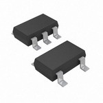
| 描述 | IC REG LDO 2.8V 0.3A TSOT23-5 |
| 产品分类 | |
| 品牌 | Analog Devices Inc |
| 数据手册 | |
| 产品图片 |
|
| 产品型号 | ADP170AUJZ-2.8-R7 |
| rohs | 无铅 / 符合限制有害物质指令(RoHS)规范要求 |
| 产品系列 | - |
| 供应商器件封装 | TSOT-5 |
| 其它名称 | ADP170AUJZ-2.8-R7DKR |
| 包装 | Digi-Reel® |
| 安装类型 | 表面贴装 |
| 封装/外壳 | SOT-23-5 细型,TSOT-23-5 |
| 工作温度 | -40°C ~ 85°C |
| 标准包装 | 1 |
| 电压-跌落(典型值) | 0.066V @ 300mA |
| 电压-输入 | 最高 3.6V |
| 电压-输出 | 2.8V |
| 电流-输出 | 300mA |
| 电流-限制(最小值) | 400mA |
| 稳压器拓扑 | 正,固定式 |
| 稳压器数 | 1 |
| 视频文件 | http://www.digikey.cn/classic/video.aspx?PlayerID=1364138032001&width=640&height=505&videoID=2245193149001 |


- 商务部:美国ITC正式对集成电路等产品启动337调查
- 曝三星4nm工艺存在良率问题 高通将骁龙8 Gen1或转产台积电
- 太阳诱电将投资9.5亿元在常州建新厂生产MLCC 预计2023年完工
- 英特尔发布欧洲新工厂建设计划 深化IDM 2.0 战略
- 台积电先进制程称霸业界 有大客户加持明年业绩稳了
- 达到5530亿美元!SIA预计今年全球半导体销售额将创下新高
- 英特尔拟将自动驾驶子公司Mobileye上市 估值或超500亿美元
- 三星加码芯片和SET,合并消费电子和移动部门,撤换高东真等 CEO
- 三星电子宣布重大人事变动 还合并消费电子和移动部门
- 海关总署:前11个月进口集成电路产品价值2.52万亿元 增长14.8%


PDF Datasheet 数据手册内容提取
300 mA, Low Quiescent Current, CMOS Linear Regulators Data Sheet ADP170/ADP171 FEATURES TYPICAL APPLICATION CIRCUITS Maximum output current: 300 mA VIN VOUT Input voltage range: 1.6 V to 3.6 V 1 VIN VOUT 5 Low quiescent current C1 ADP170 C2 I = 23 µA with 0 mA load 2 GND GND IGND = 170 µA with 300 mA load ON Low shutdown current: <1 µA OFF 3 EN NC 4 LOouwtp durto vpoolutatg veo altcacguer:a 6c6y :m ±V1% at 300 mA load 07716-001 Figure 1. ADP170 with Fixed Output Voltage, 1.8 V Up to 31 fixed-output voltage options available from 0.8 V to 3.0 V Adjustable-output voltage range VIN = 2.3V VOUT = 1.8V 1 VIN VOUT 5 0.8 V to 3.0 V (ADP171) CIN ADP171 COUT Accuracy over line, load, and temperature: ±3% 1µF 1µF Stable with small 1 µF ceramic output capacitor 2 GND R1 PSRR performance of 70 dB at 10 kHz and 73 dB at 1 kHz ON Low noise: 30 µV rms at V = 0.8 V OFF 3 EN ADJ 4 OUT CLougrriec-ncto lnimtriot lalendd e tnhaebrmlea l overload protection R2 07716-002 Compact 5-lead TSOT package Figure 2. ADP171 with Adjustable Output Voltage APPLICATIONS Mobile phones Digital camera and audio devices Portable and battery-powered equipment DSP/FPGA/microprocessor supplies Post dc-dc regulation GENERAL DESCRIPTION The ADP170/ADP171 are low voltage input, low quiescent performance and occupy minimal board space. Compared with current, low-dropout (LDO) linear regulators that operate from commodity types of LDOs, the ADP170/ADP171 provide 20 dB 1.6 V to 3.6 V and provide up to 300 mA of output current. The to 40 dB better power supply rejection ratio (PSRR) at 100 kHz, low 66 mV dropout voltage at 300 mA load improves efficiency making the ADP170/ADP171 an ideal power source for analog- and allows operation over a wide input voltage range. The low to-digital converter (ADC) mixed-signal processor systems and 23 µA of quiescent current at a 0 mA load makes the ADP170/ allowing use of smaller size bypass capacitors. In addition, low ADP171 ideal for battery-operated portable equipment. output noise performance without the need for an additional bypass capacitor further reduces printed circuit board (PCB) The ADP170 is capable of 31 fixed-output voltage options, ranging component count. from 0.8 V to 3.0 V. ADP171 is an adjustable version, which allows output voltages that range from 0.8 V to 3.0 V via an external Short-circuit protection and thermal overload protection circuits divider. The ADP170/ADP171 are optimized for stable operation prevent damage in adverse conditions. The ADP170/ADP171 with small 1 µF ceramic output capacitors. Ideal for powering are available in tiny 5-lead TSOT for the smallest footprint digital processors, the ADP170/ADP171 exhibit good transient solution to meet a variety of portable power applications. Rev. C Document Feedback Information furnished by Analog Devices is believed to be accurate and reliable. However, no responsibility is assumed by Analog Devices for its use, nor for any infringements of patents or other One Technology Way, P.O. Box 9106, Norwood, MA 02062-9106, U.S.A. rights of third parties that may result from its use. Specifications subject to change without notice. No license is granted by implication or otherwise under any patent or patent rights of Analog Devices. Tel: 781.329.4700 ©2009–2014 Analog Devices, Inc. All rights reserved. Trademarks and registered trademarks are the property of their respective owners. Technical Support www.analog.com
ADP170/ADP171 Data Sheet TABLE OF CONTENTS Features .............................................................................................. 1 Typical Performance Characteristics ..............................................7 Applications ....................................................................................... 1 Theory of Operation ...................................................................... 11 Typical Application Circuits ............................................................ 1 Applications Information .............................................................. 12 General Description ......................................................................... 1 Capacitor Selection .................................................................... 12 Revision History ............................................................................... 2 Undervoltage Lockout ............................................................... 13 Specifications ..................................................................................... 3 Enable Feature ............................................................................ 13 Input and Output Capacitor, Recommended Specifications ........ 4 Current Limit and Thermal Overload Protection ................. 14 Absolute Maximum Ratings ............................................................ 5 Thermal Considerations ............................................................ 14 Thermal Data ................................................................................ 5 Printed Circuit Board Layout Considerations ....................... 16 Thermal Resistance ...................................................................... 5 Outline Dimensions ....................................................................... 17 ESD Caution .................................................................................. 5 Ordering Guide .......................................................................... 17 Pin Configurations and Function Descriptions ........................... 6 REVISION HISTORY 1/14—Rev. B to Rev. C Changes to Ordering Guide .......................................................... 17 5/10—Rev. A to Rev. B Changes to Figure 1 and Figure 2 ................................................... 1 Updated Outline Dimensions ....................................................... 17 Changes to Ordering Guide .......................................................... 17 6/09—Rev. 0 to Rev. A Changes to Features Section............................................................ 1 Updated Outline Dimensions ....................................................... 17 1/09—Revision 0: Initial Version Rev. C | Page 2 of 20
Data Sheet ADP170/ADP171 SPECIFICATIONS V = (V + 0.4 V) or 1.6 V (whichever is greater), EN = V , I = 10 mA, C = C = 1 µF, T = 25°C, unless otherwise noted. IN OUT IN OUT IN OUT A Table 1. Parameter Symbol Conditions Min Typ Max Unit INPUT VOLTAGE RANGE V T = −40°C to +125°C 1.6 3.6 V IN J OPERATING SUPPLY CURRENT1 I I = 0 µA 23 µA GND OUT I = 0 µA, T = −40°C to +125°C 60 µA OUT J I = 1 mA 50 µA OUT I = 1 mA, T = −40°C to +125°C 100 µA OUT J I = 150 mA 130 µA OUT I = 150 mA, T = −40°C to +125°C 210 µA OUT J I = 300 mA 170 µA OUT I = 300 mA, T = −40°C to +125°C 260 µA OUT J SHUTDOWN CURRENT I EN = GND 0.1 µA GND-SD EN = GND, V = 3.6 V, T = −40°C to +85°C 2 µA IN J EN = GND, V = 3.6 V, T = 85°C to 125°C 25 µA IN J FIXED-OUTPUT VOLTAGE ACCURACY V I = 10 mA −1 +1 % OUT OUT 1 mA < I < 300 mA, V = (V + 0.5 V) to 3.6 V −2 +2 % OUT IN OUT 1 mA < I < 300 mA, V = (V + 0.5 V) to 3.6 V, −3 +3 % OUT IN OUT T = −40°C to +125°C J ADJUSTABLE-OUTPUT VOLTAGE ACCURACY (ADP171)2 V I = 10 mA 0.495 0.5 0.505 V ADJ OUT 1 mA < I < 300 mA, V = (V + 0.5 V) to 3.6 V 0.490 0.510 V OUT IN OUT 1 mA < I < 300 mA, V = (V + 0.5 V) to 3.6 V, 0.485 0.515 V OUT IN OUT T = −40°C to +125°C J ADJ INPUT BIAS CURRENT (ADP171) ADJ 1.6 V ≤ V ≤ 3.6 V, ADJ connected to VOUT 15 nA I-BIAS IN LINE REGULATION ∆V /∆V V = (V + 0.5 V) to 3.6 V, T = −40°C to +125°C −0.25 +0.25 %/V OUT IN IN OUT J LOAD REGULATION3 ∆V /∆I I = 1 mA to 300 mA 0.001 %/mA OUT OUT OUT I = 1 mA to 300 mA, T = −40°C to +125°C 0.007 %/mA OUT J DROPOUT VOLTAGE4 V I = 10 mA, V ≥ 1.8 V 2 mV DROPOUT OUT OUT I = 10 mA, V ≥ 1.8 V, T = −40°C to +125°C 7 mV OUT OUT J I = 150 mA, V ≥ 1.8 V 33 mV OUT OUT I = 150 mA, V ≥ 1.8 V, T = −40°C to +125°C 70 mV OUT OUT J I = 300 mA, V ≥ 1.8 V 66 mV OUT OUT I = 300 mA, V ≥ 1.8 V, T = −40°C to +125°C 135 mV OUT OUT J START-UP TIME5 t V = 1.8 V 120 µs START-UP OUT CURRENT-LIMIT THRESHOLD6 I 400 450 800 mA LIMIT THERMAL SHUTDOWN Thermal Shutdown Threshold TSSD TJ rising 150 °C Thermal Shutdown Hysteresis TSSD-HYS 15 °C EN INPUT Logic High Voltage V 1.6 V ≤ V ≤ 3.6 V 1.2 V IH IN Logic Low Voltage V 1.6 V ≤ V ≤ 3.6 V 0.4 V IL IN Leakage Current Voltage V EN = VIN or GND 0.1 µA I-LEAKAGE EN = VIN or GND, T = −40°C to +125°C 1 µA J UNDERVOLTAGE LOCKOUT UVLO Input Voltage Rising UVLO T = −40°C to +125°C 1.5 V RISE J Input Voltage Falling UVLO T = −40°C to +125°C 0.7 V FALL J Hysteresis UVLO 80 mV HYS Rev. C | Page 3 of 20
ADP170/ADP171 Data Sheet Parameter Symbol Conditions Min Typ Max Unit OUTPUT NOISE OUT 10 Hz to 100 kHz, V = 3.6 V, V = 3.0 V 72 µV rms NOISE IN OUT 10 Hz to 100 kHz, V = 3.6 V, V = 1.8 V 50 µV rms IN OUT 10 Hz to 100 kHz, V = 3.6 V, V = 1.2 V 40 µV rms IN OUT 10 Hz to 100 kHz, V = 3.6 V, V = 0.8 V 30 µV rms IN OUT POWER SUPPLY REJECTION RATIO PSRR 1 kHz, V = 3.6 V, I = 10 mA, V = 0.8 V 73 dB IN OUT OUT 10 kHz, V = 3.6 V, I = 10 mA, V = 0.8 V 70 dB IN OUT OUT 10 kHz, V = (V + 1 V), I = 10 mA to 300 mA 50 dB IN OUT OUT 100 kHz, V = (V + 1 V), I = 10 mA to 300 mA 47 dB IN OUT OUT 1 The current from the external resistor divider network in the case of adjustable voltage output (as with the ADP171) should be subtracted from the ground current measured. 2 Accuracy when VOUT is connected directly to ADJ. When the VOUT voltage is set by external feedback resistors, the absolute accuracy in adjust mode depends on the tolerances of resistors used. 3 Based on an end-point calculation using 1 mA and 300 mA loads. See Figure 6 for typical load regulation performance for loads less than 1 mA. 4 Applies only for output voltages above 1.6 V. Dropout voltage is defined as the input-to-output voltage differential when the input voltage is set to the nominal output voltage. 5 Start-up time is defined as the time between the rising edge of EN and VOUT being at 90% of its nominal value. 6 Current-limit threshold is defined as the current at which the output voltage drops to 90% of the specified typical value. For example, the current limit for a 3.0 V output voltage is defined as the current that causes the output voltage to drop to 90% of 3.0 V, or 2.7 V. INPUT AND OUTPUT CAPACITOR, RECOMMENDED SPECIFICATIONS Table 2. Parameter Symbol Conditions Min Typ Max Unit MINIMUM INPUT AND OUTPUT C T = −40°C to +125°C 0.45 µF MIN J CAPACITANCE1 CAPACITOR ESR R T = −40°C to +125°C 0.001 1 Ω ESR J 1 The minimum input and output capacitance should be greater than 0.45 µF over the full range of operating conditions. The full range of operating conditions in the application must be considered during device selection to ensure that the minimum capacitance specification is met. X7R and X5R type capacitors are recommended; Y5V and Z5U capacitors are not recommended for use with any LDO. Rev. C | Page 4 of 20
Data Sheet ADP170/ADP171 ABSOLUTE MAXIMUM RATINGS maximum power dissipation exists, close attention to thermal Table 3. board design is required. The value of θ may vary, depending Parameter Rating JA on PCB material, layout, and environmental conditions. The VIN to GND −0.3 V to +3.6 V specified values of θ are based on a 4-layer, 4 in. × 3 in. PCB. VOUT to GND −0.3 V to VIN JA Refer to JESD 51-7 for detailed information regarding board EN to GND −0.3 V to +3.6 V construction. Storage Temperature Range −65°C to +150°C Operating Junction Temperature Range −40°C to +125°C ΨJB is the junction-to-board thermal characterization parameter Operating Ambient Temperature Range −40°C to +85°C with units of °C/W. The ΨJB of the package is based on modeling Soldering Conditions JEDEC J-STD-020 and calculation using a 4-layer board. The Guidelines for Reporting and Using Electronic Package Thermal Information: JESD51-12 states that thermal characterization parameters are not the same Stresses above those listed under absolute maximum ratings as thermal resistances. Ψ measures the component power flowing may cause permanent damage to the device. This is a stress JB through multiple thermal paths rather than a single path as in rating only and functional operation of the device at these or thermal resistance, θ . Therefore, Ψ thermal paths include any other conditions above those indicated in the operational JB JB convection from the top of the package as well as radiation from section of this specification is not implied. Exposure to absolute the package—factors that make Ψ more useful in real-world maximum rating conditions for extended periods may affect JB applications. Maximum junction temperature (T) is calculated device reliability. J from the board temperature (T ) and power dissipation (P ) B D THERMAL DATA using the formula Absolute maximum ratings apply only individually, not in T = T + (P × Ψ ) J B D JB combination. The ADP170/ADP171 can be damaged when the Refer to JESD51-8 and JESD51-12 for more detailed information junction temperature limits are exceeded. Monitoring ambient about Ψ . temperature does not guarantee that T is within the specified JB J temperature limits. In applications with high power dissipation THERMAL RESISTANCE and poor thermal resistance, the maximum ambient temperature θ and Ψ are specified for the worst-case conditions, that is, a JA JB may have to be derated. device soldered in a circuit board for surface-mount packages. In applications with moderate power dissipation and low PCB Table 4. Thermal Resistance thermal resistance, the maximum ambient temperature can Package Type θ Ψ Unit exceed the maximum limit as long as the junction temperature JA JB 5-Lead TSOT 170 43 °C/W is within specification limits. The junction temperature (T) of J the device is dependent on the ambient temperature (T ), the A power dissipation of the device (P ), and the junction-to- ESD CAUTION D ambient thermal resistance of the package (θ ). JA Maximum junction temperature (T) is calculated from the J ambient temperature (T ) and power dissipation (P ) using the A D following formula: T = T + (P × θ ) J A D JA Junction-to-ambient thermal resistance (θJA) of the package is based on modeling and calculation using a 4-layer board. The junction-to-ambient thermal resistance is highly dependent on the application and board layout. In applications where high Rev. C | Page 5 of 20
ADP170/ADP171 Data Sheet PIN CONFIGURATIONS AND FUNCTION DESCRIPTIONS VIN 1 5 VOUT VIN 1 5 VOUT ADP170 ADP171 GND 2 TOP VIEW GND 2 TOP VIEW (Not to Scale) (Not to Scale) NECN = N3O CONNECT 4 NC 07716-003 EN 3 4 ADJ 07716-004 Figure 3. ADP170 5-Lead TSOT Figure 4. ADP171 5-Lead TSOT Table 5. Pin Function Descriptions Pin No. ADP170 ADP171 Mnemonic Description 1 1 VIN Regulator Input Supply. Bypass VIN to GND with a 1 μF or greater capacitor. 2 2 GND Ground. 3 3 EN Enable Input. Drive EN high to turn on the regulator; drive EN low to turn off the regulator. For automatic startup, connect EN to VIN. 4 NC No Connect. Not connected internally. 4 ADJ Adjust. A resistor divider from VOUT to ADJ sets the output voltage. 5 5 VOUT Regulated Output Voltage. Bypass VOUT to GND with a 1 μF or greater capacitor. Rev. C | Page 6 of 20
Data Sheet ADP170/ADP171 TYPICAL PERFORMANCE CHARACTERISTICS V = 3.6 V, V = 1.8 V, I = 10 mA, C = C = 1 μF, T = 25°C, unless otherwise noted. IN OUT OUT IN OUT A 1.810 200 180 1.805 160 ILOAD = 300mA 1.800 µA) 140 V) 1.795 RENT ( 120 ILOAD = 100mA (OUT1.790 CUR 100 V D 1.785 UN 80 ILOAD = 10mA 1.780 IILLOOAADD == 110m0AµA GRO 60 ILOAD = 1mA 11..777705 IIIILLLLOOOOAAAADDDD ==== 11230000m000mmmAAAA 07716-005 24000 IILLOOAADD == 1100µ0µAA 07716-008 –40 –5 25 85 125 –40 –5 25 85 125 JUNCTION TEMPERATURE (°C) JUNCTION TEMPERATURE (°C) Figure 5. Output Voltage vs. Junction Temperature Figure 8. Ground Current vs. Junction Temperature 1.804 180 160 1.803 140 A) µ 1.802 T ( 120 N V) RE 100 V (OUT1.801 D CUR 80 N U 1.800 O 60 R G 40 1.799 1.798 07716-006 200 07716-009 0.01 0.1 1 10 100 1k 0.01 0.1 1 10 100 1k LOAD CURRENT (mA) LOAD CURRENT (mA) Figure 6. Output Voltage vs. Load Current Figure 9. Ground Current vs. Load Current 1.805 180 1.804 160 ILOAD = 300mA 140 1.803 A) ILOAD = 100mA µ T (120 N V (V)OUT11..880012 D CURRE10800 ILOAD = 10mA N U O 60 1.800 GR ILOAD = 1mA 40 ILOAD = 100µA 1.799 1.798 IILLOOAADD == 110m0AµA IILLOOAADD == 1100m0mAA IILLOOAADD == 230000mmAA 07716-007 200 ILOAD = 10µA 07716-010 2.1 2.3 2.5 2.7 2.9 3.1 3.3 3.5 2.1 2.3 2.5 2.7 2.9 3.1 3.3 3.5 VIN (V) VIN (V) Figure 7. Output Voltage vs. Input Voltage Figure 10. Ground Current vs. Input Voltage Rev. C | Page 7 of 20
ADP170/ADP171 Data Sheet 5.0 400 4.5 VIN =2.1V VIN =2.3V 350 4.0 VIN =2.7V RENT (µA) 33..50 VVVVIIIINNNN ==== 3323....9245VVVV ENT (µA) 320500 CUR 2.5 VIN =3.6V URR 200 SHUTDOWN 21..05 GROUND C 115000 IILLOOAADD == 11m0mAA 1.0 ILOAD = 100mA 0.05 07716-011 500 IILLOOAADD == 230000mmAA 07716-014 –50 –25 0 25 50 75 100 125 1.5 1.6 1.7 1.8 1.9 2.0 TEMPERATURE (°C) VIN (V) Figure 11. Shutdown Current vs. Temperature at Various Input Voltages Figure 14. Ground Current vs. Input Voltage (In Dropout) 70 –30 300mA 60 TA = 25°C –40 210000mmAA V) 10mA m50 1mA E ( –50 G TA40 dB) OL R ( –60 V S UT 30 PS O OP –70 R20 D –80 100 07716-012 –90 07716-015 0.1 1 10 100 1k 10 100 1k 10k 100k 1M 10M LOAD CURRENT (mA) FREQUENCY (Hz) Figure 12. Dropout Voltage vs. Load Current Figure 15. Power Supply Rejection Ratio vs. Frequency, VOUT = 0.8 V 1.85 –30 300mA 1.80 200mA –40 100mA 10mA 1.75 1mA –50 V (V)OUT 11..7605 IIILLLOOOAAADDD === 1110m0m0AmAA PSSR (dB) –60 ILOAD = 200mA 1.60 ILOAD = 300mA –70 1.55 –80 1.50 07716-013 –90 07716-016 1.55 1.60 1.65 1.70 1.75 1.80 1.85 1.90 10 100 1k 10k 100k 1M 10M VIN (V) FREQUENCY (Hz) Figure 13. Output Voltage vs. Input Voltage (in Dropout) Figure 16. Power Supply Rejection Ratio vs. Frequency, VOUT = 1.8 V Rev. C | Page 8 of 20
Data Sheet ADP170/ADP171 –30 70 3V –40 60 50 –50 V) dB) E (µ 40 1.8V PSSR ( –60 320000mmAA S NOIS 30 100mA M –70 10mA R 0.8V 1mA 20 –80 10 –90 07716-017 0 07716-020 10 100 1k 10k 100k 1M 10M 0.001 0.01 0.1 1 10 100 1000 FREQUENCY (Hz) LOAD CURRENT (mA) Figure 17. Power Supply Rejection Ratio vs. Frequency, VOUT = 3.0 V Figure 20. RMS Noise vs. Load Current and Output Voltage –30 3V, 1mA 1.8V, 1mA ILOAD 0.8V, 1mA –40 3V, 300mA 1mA TO 300mA LOAD STEP, 1.8V, 300mA 2.5A/µs 0.8V, 300mA 1 –50 B) d R ( –60 SS VOUT P 2 –70 –80 –90 07716-118 VVIONU =T 3=. 61V.8V 07716-121 10 100 1k 10k 100k 1M 10M CH1 200mA Ω CH2 50.0mV BW M40.00µs A CH1 124mA FREQUENCY (Hz) T 160.680µs Figure 18. Power Supply Rejection Ratio vs. Frequency, Various Output Figure 21. Load Transient Response, CIN and COUT = 1 μF Voltages and Load Currents 10 ILOAD 1mA TO 300mA LOAD STEP, 2.5A/µs 1 1 0.8V Hz) 1.8V V/rt ( 3.0V VOUT µ 2 0.1 0.0110 VCILIOONUA =TD 3==. 6 11Vµ01Fm00A 1k 10k 10007716-019k CH1 200mA Ω CH2 50.0mV BW M40.0µs A VV CIONHU 1=T 3= . 612V.084VmA07716-122 FREQUENCY (Hz) T 159.800µs Figure 19. Output Noise Spectrum Figure 22. Load Transient Response, CIN and COUT = 4.7 μF Rev. C | Page 9 of 20
ADP170/ADP171 Data Sheet VIN VIN 2.6V TO 3.6V INPUT VOLTAGE STEP, 2V/µs 2.6V TO 3.6V INPUT VOLTAGE STEP 2V/µs 1 1 2 VOUT 2 VOUT CVOINU =T =C O1U.8TV = 1µF 07716-123 CVOINU =T =C O1U.8TV = 1µF 07716-124 CH1 1.00V CH2 10.0mV M10.0µs A CH1 2.94V CH1 1.00V CH2 10.0mV BW M10.0µs A CH1 2.94V T 39.3000% T 39.3000µs Figure 23. Line Transient Response, Load Current = 1 mA Figure 24. Line Transient Response, Load Current = 300 mA Rev. C | Page 10 of 20
Data Sheet ADP170/ADP171 THEORY OF OPERATION The ADP170/ADP171 are low quiescent current, low-dropout Internally, the ADP170/ADP171 consist of a reference, an error linear regulators that operate from 1.6 V to 3.6 V and can provide amplifier, a feedback voltage divider, and a PMOS pass transistor. up to 300 mA of output current. Drawing a low 170 µA of quies- Output current is delivered via the PMOS pass device, which is cent current (typical) at full load makes the ADP170/ADP171 controlled by the error amplifier. The error amplifier compares ideal for battery-operated portable equipment. Shutdown current the reference voltage with the feedback voltage from the output consumption is typically 100 nA. and amplifies the difference. If the feedback voltage is lower than the reference voltage, the gate of the PMOS device is pulled lower, Optimized for use with small 1 µF ceramic capacitors, the allowing more current to pass and increasing the output voltage. ADP170/ADP171 provide excellent transient performance. If the feedback voltage is higher than the reference voltage, the ADP170 gate of the PMOS device is pulled higher, allowing less current VIN VOUT to pass and decreasing the output voltage. The adjustable ADP171 has an output voltage range of 0.8 V to 3.0 V. The output voltage is set by the ratio of two external resistors, SHORT CIRCUIT, R1 GND UVLOAND as shown in Figure 2. The device servos the output to maintain THERMAL PROTECT the voltage at the ADJ pin at 0.5 V referenced to ground. The current in R1 is then equal to 0.5 V/R2 and the current in R1 is the current in R2 plus the ADJ pin bias current. The ADJ pin EN SHUTDOWN 0.5V REFERENCE R2 bias current, 15 nA at 25°C, flows through R1 into the ADJ pin. 07716-021 The output voltage can be calculated using the equation: NOTES V = 0.5 V(1 + R1/R2) + (ADJ )(R1) OUT I-BIAS 1. R1AND R2ARE INTERNAL RESISTORS,AVAILABLE ON THEADP170 ONLY. The value of R1 should be less than 200 kΩ to minimize errors Figure 25. ADP170 Internal Block Diagram in the output voltage caused by the ADJ pin bias current. For ADP171 example, when R1 and R2 each equal 200 kΩ, the output voltage VIN VOUT is 1.0 V. The output voltage error introduced by the ADJ pin bias current is 3 mV or 0.3%, assuming a typical ADJ pin bias current of 15 nA at 25°C. SHORT CIRCUIT, Note that in shutdown, the output is turned off and the divider GND UVLOAND THERMAL current is zero. PROTECT The ADP170/ADP171 use the EN pin to enable and disable the ADJ VOUT pin under normal operating conditions. When EN is high, EN SHUTDOWN 0.5V REFERENCE VOUT turns on; when EN is low, VOUT turns off. For automatic 07716-022 startup, EN can be tied to VIN. Figure 26. ADP171 Internal Block Diagram Rev. C | Page 11 of 20
ADP170/ADP171 Data Sheet APPLICATIONS INFORMATION CAPACITOR SELECTION Input Bypass Capacitor Output Capacitor Connecting a 1 μF capacitor from VIN to GND reduces the circuit sensitivity to the printed circuit board (PCB) layout, The ADP170/ADP171 are designed for operation with small, especially when long input traces or high source impedance space-saving ceramic capacitors but will function with most are encountered. If greater than 1 μF of output capacitance is commonly used capacitors as long as care is taken with regard required, the input capacitor should be increased to match it. to the effective series resistance (ESR) value. The ESR of the output capacitor affects the stability of the LDO control loop. Input and Output Capacitor Properties A minimum of 1 μF capacitance with an ESR of 1 Ω or less is Any good quality ceramic capacitor can be used with the recommended to ensure stability of the ADP170/ADP171. The ADP170/ADP171, as long as it meets the minimum capacitance transient response to changes in load current is also affected by and maximum ESR requirements. Ceramic capacitors are manu- output capacitance. Using a larger value of output capacitance factured with a variety of dielectrics, each with different behavior improves the transient response of the ADP170/ADP171 to over temperature and applied voltage. Capacitors must have a large changes in load current. Figure 27 and Figure 28 show the dielectric adequate to ensure the minimum capacitance over the transient responses for output capacitance values of 1 μF and necessary temperature range and dc bias conditions. A X5R or X7R 4.7 μF, respectively. dielectric with a voltage rating of 6.3 V or 10 V is recommended. ILOAD The Y5V and Z5U dielectrics are not recommended, due to their 1mA TO 300mA LOAD STEP, poor temperature and dc bias characteristics. 2.5A/µs Figure 29 depicts the capacitance vs. bias voltage characteristics 1 of a 0402, 1 μF, 10 V X5R capacitor. The variance of a capacitor is strongly influenced by the capacitor size and voltage rating. In general, a capacitor in a larger package or higher voltage rating will exhibit less capacitance variance over bias voltage. The 2 temperature variation of the X5R dielectric is about ±15% over the −40°C to +85°C temperature range and is not a function of VOUT package or voltage rating. CVOINU =T =C O1U.8TV = 1µF 07716-125 1.2 CH1 200mA Ω CH2 50.0mV BW M200ns A CH1 112mA T 500.000ns 1.0 Figure 27. Output Transient Response, COUT = 1 μF F) 0.8 µ E ( ILOAD NC 1mA TO 300mA LOAD STEP, TA 0.6 2.5A/µs CI 1 A P CA 0.4 0.2 2 0 07716-025 VOUT 0 2 4 6 8 10 BIAS VOLTAGE (V) Figure 29. Capacitance vs. Bias Voltage Characteristics CVOINU =T =C O1U.8TV = 4.7µF 07716-126 Use Equation 1 to determine the worst-case capacitance CH1 200mA Ω CH2 50.0mV BW M200ns A CH1 108mA accounting for capacitor variation over temperature, T 500.000ns component tolerance, and voltage. Figure 28. Output Transient Response, COUT = 4.7 μF C = C × (1 − TEMPCO) × (1 − TOL) (1) EFF BIAS where: C is the effective capacitance at the operating voltage. BIAS TEMPCO is the worst-case capacitor temperature coefficient. TOL is the worst-case component tolerance. Rev. C | Page 12 of 20
Data Sheet ADP170/ADP171 In this example, the worst-case temperature coefficient The EN pin active/inactive thresholds are derived from the VIN (TEMPCO) over −40°C to +85°C is assumed to be 15% for an voltage. Therefore, these thresholds vary with changing input X5R dielectric. The tolerance of the capacitor (TOL) is assumed voltage. Figure 31 shows typical EN active/inactive thresholds to be 10%, and C is 0.94 μF at 1.8 V, as shown in Figure 29. when the input voltage varies from 1.6 V to 3.6 V. BIAS Substituting these values in Equation 1 yields 1.2 CEFF = 0.94 μF × (1 − 0.15) × (1 − 0.1) = 0.719 μF 1.1 Therefore, the capacitor chosen in this example meets the V) S (1.0 EN ACTIVE minimum capacitance requirement of the LDO over temper- D L ature and tolerance at the chosen output voltage. HO0.9 S E To guarantee the performance of the ADP170/ADP171, it is TR0.8 N imperative that the effects of dc bias, temperature, and toler- AL E0.7 EN INACTIVE ances on the behavior of the capacitors are evaluated for each C PI application. TY0.6 UThNe DAEDRPV17O0/LATDAPG17E1 L hOavCeK anO iUntTe rnal undervoltage lockout 00..45 07716-129 0 5 0 5 0 5 0 5 0 5 0 5 0 5 0 circuit that disables all inputs and the output when the input 1.5 1.6 1.8 1.9 2.1 2.2 2.4 2.5 2.7 2.8 3.0 3.1 3.3 3.4 3.6 voltage is less than approximately 1.2 V. This ensures that the VIN(V) ADP170/ADP171 inputs and the output behave in a predictable Figure 31. Typical EN Pin Thresholds vs. Input Voltage manner during power-up. The ADP170/ADP171 utilize an internal soft start to limit the ENABLE FEATURE inrush current when the output is enabled. The start-up time for the 1.8 V option is approximately 120 μs from the time the The ADP170/ADP171 use the EN pin to enable and disable the EN active threshold is crossed to when the output reaches 90% VOUT pin under normal operating conditions. As shown in of its final value. As shown in Figure 32, the start-up time is Figure 30, when a rising voltage on EN crosses the active dependent on the output voltage setting. threshold, VOUT turns on. When a falling voltage on EN crosses the inactive threshold, VOUT turns off. 3.5 EN VOUT= 3.0V 3.0 2.5 VOUT= 1.8V 2.0 VOUT= 0.8V OUT 12 V 1.5 1.0 0.5 07716-130 0 07716-230 CH1 1.00V FigCuHre2 31.20.0 TVypicBaWl StaMTr 2t 0 - U.709pµ.s8 T0i0m0Aµe s CH1 2.72V 0 0.2 0.4 0.6 0.8 1.0 1.2 1.4 1.6 VEN Figure 30. ADP170/ADP171 Typical EN Pin Operation As shown in Figure 30, the EN pin has hysteresis built in. This prevents on/off oscillations that can occur due to noise on the EN pin as it passes through the threshold points. Rev. C | Page 13 of 20
ADP170/ADP171 Data Sheet CURRENT LIMIT AND THERMAL OVERLOAD The junction temperature of the ADP170/ADP171 can be PROTECTION calculated from the following equation: The ADP170/ADP171 are protected against damage due to T = T + (P × θ ) (2) J A D JA excessive power dissipation by current and thermal overload where: protection circuits. The ADP170/ADP171 are designed to limit T is the ambient temperature. A the current when the output load reaches 450 mA (typical). P is the power dissipation in the die, given by D When the output load exceeds 450 mA, the output voltage is reduced to maintain a constant current limit. PD = [(VIN − VOUT) × ILOAD] + (VIN × IGND) (3) Thermal overload protection is included, which limits the junction where: temperature to a maximum of 150°C (typical). Under extreme ILOAD is the load current. conditions (that is, high ambient temperature and power dissip- IGND is the ground current. ation), when the junction temperature starts to rise above 150°C, VIN and VOUT are input and output voltages, respectively. the output is turned off, reducing the output current to 0. When Power dissipation due to ground current is quite small and can the junction temperature drops below 135°C, the output is turned be ignored. Therefore, the junction temperature equation on again and output current is restored to its nominal value. simplifies to the following: Consider the case where a hard short from VOUT to GND occurs. T = T + {[(V − V ) × I ] × θ } (4) J A IN OUT LOAD JA At first, the ADP170/ADP171 will limit the current so that only As shown in Equation 4, for a given ambient temperature, input 450 mA is conducted into the short. If self-heating of the junction to output voltage differential, and continuous load current, is great enough to cause its temperature to rise above 150°C, there exists a minimum copper size requirement for the PCB to thermal shutdown will activate, turning off the output and ensure that the junction temperature does not rise above 125°C. reducing the output current to 0. As the junction temperature Figure 33 to Figure 38 show junction temperature calculations cools and drops below 135°C, the output turns on and conducts for different ambient temperatures, load currents, V to V 450 mA into the short, again causing the junction temperature IN OUT differentials, and areas of PCB copper. to rise above 150°C. This thermal oscillation between 135°C 140 and 150°C causes a current oscillation between 450 mA and 0 mA, TJ MAX which continues as long as the short remains at the output. 120 Current and thermal limit protections are intended to protect E (°C) 100 ILOAD = 300mA the device against accidental overload conditions. R U T A THERMAL CONSIDERATIONS ER 80 ILOAD = 150mA P M To guarantee reliable operation, the junction temperature of the E T 60 ADP170/ADP171 must not exceed 125°C. To ensure the junction ON ILOAD = 100mA TI temperature stays below this maximum value, the user needs to NC 40 ILOAD = 25mA U be aware of the parameters that contribute to junction temperature J cdhisasnipgaetsi.o Tn hines teh pe aproawmeert edresv iincec,l uadned athmebrmienalt rteesmisptaenracteus rbee, tpwoewener 200 ILOAD = 1mA ILOAD = 10mA 07716-028 the junction and ambient air (θ ). The θ number is dependent 0.5 1.0 1.5 2.0 2.5 3.0 JA JA on the package assembly compounds used and the amount of VOUT – VIN (V) copper to which the GND pin of the package is soldered on the Figure 33. 500 mm2 of PCB Copper, TA = 25°C PCB. Table 6 shows typical θ values of the 5-lead TSOT package 140 JA for various PCB copper sizes. TJ MAX 120 Table 6. Typical θJA Values E (°C) 100 ILOAD = 300mA Copper Size (mm2) θJA (°C/W) UR T 01 170 RA 80 ILOAD = 150mA E 50 152 MP E 100 146 ON T 60 ILOAD = 100mA 300 134 TI 500 131 UNC 40 ILOAD = 25mA J 1 Device soldered to minimum size pin traces. 200 ILOAD = 1mA ILOAD = 10mA 07716-029 0.5 1.0 1.5 2.0 2.5 3.0 VOUT – VIN (V) Figure 34. 100 mm2 of PCB Copper, TA = 25°C Rev. C | Page 14 of 20
Data Sheet ADP170/ADP171 140 140 TJ MAX TJ MAX 120 120 E (°C) 100 ILOAD = 300mA E (°C) 100 ILOAD = 300mA ILOAD = 150mA R R U U T T ERA 80 ILOAD = 150mA ERA 80 ILOAD = 100mA P P EM EM ILOAD = 25mA N T 60 ILOAD = 100mA N T 60 O O CTI 40 ILOAD = 25mA CTI 40 UN UN ILOAD = 1mA ILOAD = 10mA J J 200 ILOAD = 1mA ILOAD = 10mA 07716-030 200 07716-033 0.5 1.0 1.5 2.0 2.5 3.0 0.5 1.0 1.5 2.0 2.5 3.0 VIN – VOUT (V) VOUT – VIN (V) Figure 35. 0 mm2 of PCB Copper, TA = 25°C Figure 38. 0 mm2 of PCB Copper, TA = 50°C 140 In cases where board temperature is known, use the thermal TJ MAX characterization parameter, Ψ , to estimate the junction tem- JB 120 C) ILOAD = 300mA perature rise (see Figure 39). Maximum junction temperature RE (° 100 ILOAD = 150mA (TJ) is calculated from the board temperature (TB) and power ATU dissipation (PD) using the following formula: PER 80 ILOAD = 100mA TJ = TB + (PD × ΨJB) (5) M N TE 60 ILOAD = 25mA The typical value of ΨJB is 42.8°C/W for the 5-lead TSOT package. O TI 140 C 40 UN ILOAD = 1mA ILOAD = 10mA J 120 2000.5 1.0 1.5 2.0 2.5 3.007716-031 TURE (°C) 100 A VOUT – VIN (V) ER 80 P 140 Figure 36. 500 mm2 of PCB Copper, TA = 50°C ON TEM 60 IILLOOAADD == 110mmAA IILLOOAADD == 215500mmAA 120 TJ MAX UNCTI 40 IILLOOAADD == 5100m0mAA ITLJO MADA X= 300mA C) ILOAD = 300mA J ATURE (° 100 ILOAD = 150mA 200 07716-034 ER 80 ILOAD = 100mA 0.4 0.8 1.2 1.6 2.0 2.4 2.8 MP VIN – VOUT (V) N TE 60 ILOAD = 25mA Figure 39. TSOT, TA = 85°C O TI C 40 UN ILOAD = 1mA ILOAD = 10mA J 200 07716-032 0.5 1.0 1.5 2.0 2.5 3.0 VOUT – VIN (V) Figure 37. 100 mm2 of PCB Copper, TA = 50°C Rev. C | Page 15 of 20
ADP170/ADP171 Data Sheet PRINTED CIRCUIT BOARD LAYOUT GND GND CONSIDERATIONS ANALOG DEVICES ADP171-x.x-EVALZ Heat dissipation from the package can be improved by increasing the amount of copper attached to the pins of the ADP170/ADP171. However, as can be seen from Table 6, a C1 C2 U1 point of diminishing returns is eventually reached, beyond which an increase in the copper size does not yield significant heat dissipation benefits. Place the input capacitor as close as possible to the VIN and GND pins. Place the output capacitor as close as possible to the J1 VOUT and GND pins. Use of 0402 or 0603 size capacitors and R1 resistors achieves the smallest possible footprint solution on VIN VOUT boards where area is limited. R2 GND GND ANALOG DEVICES ADP170-x.x-EVALZ GND EN GND 07716-036 Figure 41. Example ADP171 PCB Layout C1 C2 U1 J1 VIN VOUT GND EN GND 07716-035 Figure 40. Example ADP170 PCB Layout Rev. C | Page 16 of 20
Data Sheet ADP170/ADP171 OUTLINE DIMENSIONS 2.90 BSC 5 4 1.60 BSC 2.80 BSC 1 2 3 0.95 BSC 1.90 *0.90 MAX BSC 0.70 MIN *1.00 MAX 0.20 0.08 8° 0.10 MAX 0.50 SEATING 4° 0.60 0.30 PLANE 0° 0.45 0.30 *CTHOEM PELXICAENPTT TIOON J OEDF EPCA CSTKAANGDEA HREDIGS HMTO A-1N9D3 -TAHBICWKINTHESS. 100708-A Figure 42. 5-Lead Thin Small Outline Transistor Package [TSOT] (UJ-5) Dimensions show in millimeters ORDERING GUIDE Package Model1 Temperature Range Output Voltage (V)2 Package Description Option Branding ADP170AUJZ-1.2-R7 –40°C to +125°C 1.2 5-Lead TSOT UJ-5 L8E ADP170AUJZ-1.25-R7 –40°C to +125°C 1.25 5-Lead TSOT UJ-5 LQD ADP170AUJZ-1.5-R7 –40°C to +125°C 1.5 5-Lead TSOT UJ-5 L8F ADP170AUJZ-1.8-R7 –40°C to +125°C 1.8 5-Lead TSOT UJ-5 L8G ADP170AUJZ-2.5-R7 –40°C to +125°C 2.5 5-Lead TSOT UJ-5 L8H ADP170AUJZ-2.8-R7 –40°C to +125°C 2.8 5-Lead TSOT UJ-5 L8P ADP171AUJZ-R7 –40°C to +125°C 0.8 to 3.0 (Adjustable) 5-Lead TSOT UJ-5 L9A ADP170-1.8-EVALZ Evaluation Board ADP171-EVALZ Evaluation Board 1 Z = RoHS Compliant Part. 2 For additional voltage options, contact your local Analog Devices, Inc., sales or distribution representative. Rev. C | Page 17 of 20
ADP170/ADP171 Data Sheet NOTES Rev. C | Page 18 of 20
Data Sheet ADP170/ADP171 NOTES Rev. C | Page 19 of 20
ADP170/ADP171 Data Sheet NOTES ©2009–2014 Analog Devices, Inc. All rights reserved. Trademarks and registered trademarks are the property of their respective owners. D07716-0-1/14(C) Rev. C | Page 20 of 20