ICGOO在线商城 > 集成电路(IC) > PMIC - 稳压器 - DC DC 开关稳压器 > ADP1613ARMZ-R7
 Datasheet下载
- 型号: ADP1613ARMZ-R7
- 制造商: Analog
- 库位|库存: xxxx|xxxx
- 要求:
| 数量阶梯 | 香港交货 | 国内含税 |
| +xxxx | $xxxx | ¥xxxx |
查看当月历史价格
查看今年历史价格
ADP1613ARMZ-R7产品简介:
ICGOO电子元器件商城为您提供ADP1613ARMZ-R7由Analog设计生产,在icgoo商城现货销售,并且可以通过原厂、代理商等渠道进行代购。 ADP1613ARMZ-R7价格参考。AnalogADP1613ARMZ-R7封装/规格:PMIC - 稳压器 - DC DC 开关稳压器, 可调式 升压,SEPIC 开关稳压器 IC 正 2.5V 1 输出 2A(开关) 8-TSSOP,8-MSOP(0.118",3.00mm 宽)。您可以下载ADP1613ARMZ-R7参考资料、Datasheet数据手册功能说明书,资料中有ADP1613ARMZ-R7 详细功能的应用电路图电压和使用方法及教程。
ADP1613ARMZ-R7 是由 Analog Devices Inc. 生产的一款高性能 DC-DC 开关稳压器,属于 PMIC(电源管理集成电路)类别。它主要应用于需要高效、紧凑且稳定电源解决方案的场景中。以下是其典型应用场景:

 1. 通信设备
   ADP1613ARMZ-R7 可用于通信基站、路由器和交换机等设备中,提供稳定的电源输出。这些设备通常需要在较宽的工作电压范围内保持高效率,并且对电源的瞬态响应要求较高。ADP1613ARMZ-R7 的宽输入电压范围(2.9V 至 20V)和快速瞬态响应特性使其非常适合此类应用。

 2. 工业自动化
   在工业控制系统中,如 PLC(可编程逻辑控制器)、传感器和执行器等,ADP1613ARMZ-R7 可以为这些设备提供可靠的电源支持。它能够在恶劣的工业环境中工作,具备良好的抗干扰能力和稳定性,确保系统的可靠运行。

 3. 消费电子
   对于便携式消费电子产品,如平板电脑、智能手表和可穿戴设备,ADP1613ARMZ-R7 提供了高效的小型化电源解决方案。其高集成度和低静态电流特性有助于延长电池寿命,同时保持较小的电路板占用面积。

 4. 汽车电子
   在汽车电子系统中,ADP1613ARMZ-R7 可以为车载信息娱乐系统、导航设备和传感器等提供稳定的电源。它能够承受汽车电气系统中的电压波动,并提供高效的电源转换,确保系统的正常运行。

 5. 医疗设备
   医疗设备如便携式监护仪、血糖仪和其他手持式医疗仪器也需要稳定的电源供应。ADP1613ARMZ-R7 的高精度输出电压调节和低噪声特性使其成为这些设备的理想选择,确保测量结果的准确性。

 6. 物联网 (IoT) 设备
   IoT 设备通常需要长时间运行且功耗较低,ADP1613ARMZ-R7 的高效能和低功耗特性使其适合为这些设备供电。它可以在较宽的工作温度范围内稳定工作,适应不同的环境条件。

总之,ADP1613ARMZ-R7 凭借其高效、紧凑和稳定的特点,广泛应用于各种需要高性能电源管理的领域,尤其适用于对电源效率和可靠性有较高要求的应用场景。
| 参数 | 数值 |
| 产品目录 | 集成电路 (IC)半导体 |
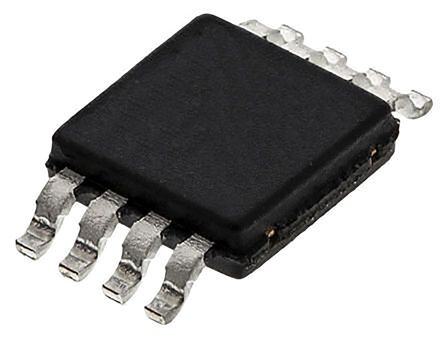
| 描述 | IC REG BOOST SEPIC ADJ 2A 8MSOP稳压器—开关式稳压器 650kHz /1.3MHz Step-Up PWM |
| 产品分类 | |
| 品牌 | Analog Devices Inc |
| 产品手册 | |
| 产品图片 |
|
| rohs | 符合RoHS无铅 / 符合限制有害物质指令(RoHS)规范要求 |
| 产品系列 | 电源管理 IC,稳压器—开关式稳压器,Analog Devices ADP1613ARMZ-R7- |
| 数据手册 | |
| 产品型号 | ADP1613ARMZ-R7 |
| PWM类型 | 电流模式 |
| 产品目录页面 | |
| 产品种类 | 稳压器—开关式稳压器 |
| 供应商器件封装 | 8-MSOP |
| 其它名称 | ADP1613ARMZ-R7CT |
| 包装 | 剪切带 (CT) |
| 同步整流器 | 无 |
| 商标 | Analog Devices |
| 安装类型 | 表面贴装 |
| 安装风格 | SMD/SMT |
| 宽度 | 3 mm |
| 封装 | Reel |
| 封装/外壳 | 8-TSSOP,8-MSOP(0.118",3.00mm 宽) |
| 封装/箱体 | MSOP-8 |
| 工作温度 | -40°C ~ 125°C |
| 工厂包装数量 | 1000 |
| 开关频率 | 650 kHz |
| 最大工作温度 | + 85 C |
| 最大输入电压 | 5.5 V |
| 最小工作温度 | - 40 C |
| 最小输入电压 | 2.5 V |
| 标准包装 | 1 |
| 电压-输入 | 2.5 V ~ 5.5 V |
| 电压-输出 | 2.5 V ~ 20 V |
| 电流-输出 | 2A |
| 类型 | 升压(升压),Sepic |
| 系列 | ADP1613 |
| 视频文件 | http://www.digikey.cn/classic/video.aspx?PlayerID=1364138032001&width=640&height=505&videoID=2245193149001 |
| 设计资源 | |
| 负载调节 | 0.1 mV/mA |
| 输出数 | 1 |
| 输出电压 | 20 V |
| 输出电流 | 2 A |
| 输出端数量 | 1 Output |
| 输出类型 | 可调式 |
| 配用 | /product-detail/zh/ADP1613-12-EVALZ/ADP1613-12-EVALZ-ND/2077083 |
| 频率-开关 | 650kHz,1.3MHz |


- 商务部:美国ITC正式对集成电路等产品启动337调查
- 曝三星4nm工艺存在良率问题 高通将骁龙8 Gen1或转产台积电
- 太阳诱电将投资9.5亿元在常州建新厂生产MLCC 预计2023年完工
- 英特尔发布欧洲新工厂建设计划 深化IDM 2.0 战略
- 台积电先进制程称霸业界 有大客户加持明年业绩稳了
- 达到5530亿美元!SIA预计今年全球半导体销售额将创下新高
- 英特尔拟将自动驾驶子公司Mobileye上市 估值或超500亿美元
- 三星加码芯片和SET,合并消费电子和移动部门,撤换高东真等 CEO
- 三星电子宣布重大人事变动 还合并消费电子和移动部门
- 海关总署:前11个月进口集成电路产品价值2.52万亿元 增长14.8%


PDF Datasheet 数据手册内容提取
650 kHz /1.3 MHz Step-Up PWM DC-to-DC Switching Converters Data Sheet ADP1612/ADP1613 FEATURES TYPICAL APPLICATION CIRCUIT Current limit L1 1.4 A for the ADP1612 2.0 A for the ADP 1613 ADP1612/ Minimum input voltage VIN ADP1613 D1 VOUT 6 VIN SW 5 1.8 V for the ADP1612 ON R1 2.5 V for the ADP1613 OFF 3 EN Pin-selectable 650 kHz or 1.3 MHz PWM frequency CIN 1.3MHz FB 2 650kHz 7 FREQ Adjustable output voltage up to 20 V (DEFAULT) R2 Adjustable soft start 8 SS COMP 1 Undervoltage lockout CSS GND RCOMP COUT T8h-leeramd aMl SshOuPt down 4 CCOMP 06772-001 Figure 1. Step-Up Regulator Configuration Supported by ADIsimPower™ design tool ADIsimPower downloadable design tools for boost, coupled- SEPIC, and SEPIC Cuk configurations APPLICATIONS TFT LCD bias supplies Portable applications Industrial/instrumentation equipment GENERAL DESCRIPTION 100 VIN = 5V The ADP1612/ADP1613 are step-up dc-to-dc switching con- 90 TfSAW = = 2 15.°3CMHz verters with an integrated power switch capable of providing an output voltage as high as 20 V. With a package height of less 80 than 1.1 mm, the ADP1612/ADP1613 are optimal for space- %) Y ( 70 constrained applications such as portable devices or thin film C N E transistor (TFT) liquid crystal displays (LCDs). FICI 60 F The ADP1612/ADP1613 operate in current mode pulse-width E 50 modulation (PWM) with up to 94% efficiency. Adjustable ADP1612, VOUT = 12V soft start prevents inrush currents when the part is enabled. 40 ADP1612, VOUT = 15V The pin-selectable switching frequency and PWM current-mode ADP1613, VOUT = 12V ADP1613, VOUT = 15V afirlctehritiencgt,u arne dal ltohwe ufoser eoxf csemllaelnl,t ctroasnt-ssiaevnitn rge sepxotenrsnea, le iansdyu ncotoisres 301 1L0OAD CURRENT (mA10)0 1k 06772-009 and capacitors. Other key features include undervoltage lockout Figure 2. ADP1612/ADP1613 Efficiency for Various Output Voltages (UVLO), thermal shutdown (TSD), and logic controlled enable. The ADP1612/ADP1613 are available in the lead-free 8-lead MSOP. Rev. D Information furnished by Analog Devices is believed to be accurate and reliable. However, no responsibility is assumed by Analog Devices for its use, nor for any infringements of patents or other One Technology Way, P.O. Box 9106, Norwood, MA 02062-9106, U.S.A. rights of third parties that may result from its use. Specifications subject to change without notice. No license is granted by implication or otherwise under any patent or patent rights of Analog Devices. Tel: 781.329.4700 www.analog.com Trademarks and registered trademarks are the property of their respective owners. Fax: 781.461.3113 ©2009–2012 Analog Devices, Inc. All rights reserved.
ADP1612/ADP1613 Data Sheet TABLE OF CONTENTS Features .............................................................................................. 1 Enable/Shutdown Control ........................................................ 12 Applications ....................................................................................... 1 Applications Information .............................................................. 13 Typical Application Circuit ............................................................. 1 ADIsimPower Design Tool ....................................................... 13 General Description ......................................................................... 1 Setting the Output Voltage ........................................................ 13 Revision History ............................................................................... 2 Inductor Selection ...................................................................... 13 Specifications ..................................................................................... 3 Choosing the Input and Output Capacitors ........................... 14 Absolute Maximum Ratings ............................................................ 4 Diode Selection ........................................................................... 14 Thermal Resistance ...................................................................... 4 Loop Compensation .................................................................. 14 Boundary Condition .................................................................... 4 Soft Start Capacitor .................................................................... 15 ESD Caution .................................................................................. 4 Typical Application Circuits ......................................................... 16 Pin Configuration and Function Descriptions ............................. 5 Step-Up Regulator ...................................................................... 16 Typical Performance Characteristics ............................................. 6 Step-Up Regulator Circuit Examples ....................................... 16 Theory of Operation ...................................................................... 11 SEPIC Converter ........................................................................ 22 Current-Mode PWM Operation .............................................. 11 TFT LCD Bias Supply ................................................................ 22 Frequency Selection ................................................................... 11 PCB Layout Guidelines .................................................................. 24 Soft Start ...................................................................................... 11 Outline Dimensions ....................................................................... 25 Thermal Shutdown (TSD) ......................................................... 12 Ordering Guide .......................................................................... 25 UnderVoltage Lockout (UVLO) ............................................... 12 REVISION HISTORY 11/12—Rev. C to Rev. D 9/09—Rev. 0 to Rev. A Changes to Choosing the Input and Output Capacitors Section Changes to Figure 45 ...................................................................... 17 and Loop Compensation Section .................................................. 14 Changes to Figure 48 and Figure 51 ............................................ 18 Changes to Figure 54 and Figure 57 ............................................ 19 7/12—Rev. B to Rev. C Changes to Figure 60 and Figure 63 ............................................ 20 Changes to Features Section............................................................. 1 Changes to Figure 66 and Figure 69 ............................................ 21 Added ADIsimPower Design Tool Section .................................. 13 Changes to Figure 72 ...................................................................... 22 Changes to Ordering Guide ........................................................... 25 Changes to Ordering Guide .......................................................... 25 4/11—Rev. A to Rev. B 4/09—Revision 0: Initial Version Changes to Features Section............................................................ 1 Changes to Reference Feedback Voltage Parameter .................... 3 Changes to Ordering Guide .......................................................... 25 Rev. D | Page 2 of 28
Data Sheet ADP1612/ADP1613 SPECIFICATIONS V = 3.6 V, unless otherwise noted. Minimum and maximum values are guaranteed for T = −40°C to +125°C. Typical values specified IN J are at T = 25°C. All limits at temperature extremes are guaranteed by correlation and characterization using standard statistical quality J control (SQC), unless otherwise noted. Table 1. Parameter Symbol Conditions Min Typ Max Unit SUPPLY Input Voltage V ADP1612 1.8 5.5 V IN ADP1613 2.5 5.5 V Quiescent Current Nonswitching State I V = 1.5 V, FREQ = V 900 1350 µA Q FB IN V = 1.5 V, FREQ = GND 700 1300 µA FB Shutdown I V = 0 V 0.01 2 µA QSHDN EN Switching State1 I FREQ = V , no load 4 5.8 mA QSW IN FREQ = GND, no load 2.2 4 mA Enable Pin Bias Current I V = 3.6 V 3.3 7 µA EN EN OUTPUT Output Voltage V V 20 V OUT IN Load Regulation I = 10 mA to 150 mA, V = 3.3 V, V = 12 V 0.1 mV/mA LOAD IN OUT REFERENCE Feedback Voltage V 1.215 1.235 1.255 V FB Line Regulation ADP1612, V = 1.8 V to 5.5 V; ADP1613, V = 2.5 V to 5.5 V 0.07 0.24 %/V IN IN ERROR AMPLIFIER Transconductance G ΔI = 4 µA 80 µA/V MEA Voltage Gain A 60 dB V FB Pin Bias Current V = 1.3 V 1 50 nA FB SWITCH SW On Resistance R I = 1.0 A 130 300 mΩ DSON SW SW Leakage Current V = 20 V 0.01 10 µA SW Peak Current Limit2 I ADP1612, duty cycle = 70% 0.9 1.4 1.9 A CL ADP1613, duty cycle = 70% 1.3 2.0 2.5 A OSCILLATOR Oscillator Frequency f FREQ = GND 500 650 720 kHz SW FREQ = V 1.1 1.3 1.4 MHz IN Maximum Duty Cycle D COMP = open, V = 1 V, FREQ = V 88 90 % MAX FB IN FREQ Pin Current I FREQ = 3.6 V 5 8 μA FREQ EN/FREQ LOGIC THRESHOLD ADP1612, V = 1.8 V to 5.5 V; ADP1613, V = 2.5 V to 5.5 V IN IN Input Voltage Low V 0.3 V IL Input Voltage High V 1.6 V IH SOFT START SS Charging Current I V = 0 V 3.4 5 6.2 µA SS SS SS Voltage V V = 1.3 V 1.2 V SS FB UNDERVOLTAGE LOCKOUT (UVLO) Undervoltage Lockout Threshold ADP1612, V rising 1.70 V IN ADP1612, V falling 1.62 V IN ADP1613, V rising 2.25 V IN ADP1613, V falling 2.16 V IN THERMAL SHUTDOWN Thermal Shutdown Threshold 150 °C Thermal Shutdown Hysteresis 20 °C 1 This parameter specifies the average current while switching internally and with SW (Pin 5) floating. 2 Current limit is a function of duty cycle. See the Typical Performance Characteristics section for typical values over operating ranges. Rev. D | Page 3 of 28
ADP1612/ADP1613 Data Sheet ABSOLUTE MAXIMUM RATINGS THERMAL RESISTANCE Table 2. Junction-to-ambient thermal resistance (θ ) of the package is Parameter Rating JA specified for the worst-case conditions, that is, a device soldered VIN, EN, FB to GND −0.3 V to +6 V in a circuit board for surface-mount packages. The junction-to- FREQ to GND −0.3 V to V + 0.3 V IN ambient thermal resistance is highly dependent on the application COMP to GND 1.0 V to 1.6 V and board layout. In applications where high maximum power SS to GND −0.3 V to +1.3 V dissipation exists, attention to thermal board design is required. SW to GND 21 V The value of θ may vary, depending on PCB material, layout, Operating Junction Temperature Range −40°C to +125°C JA and environmental conditions. Storage Temperature Range −65°C to +150°C Soldering Conditions JEDEC J-STD-020 Table 3. ESD (Electrostatic Discharge) Package Type θ θ Unit JA JC Human Body Model ±5 kV 8-Lead MSOP 2-Layer Board1 206.9 44.22 °C/W Stresses above those listed under Absolute Maximum Ratings 4-Layer Board1 162.2 44.22 °C/W may cause permanent damage to the device. This is a stress rating only; functional operation of the device at these or any 1 Thermal numbers per JEDEC standard JESD 51-7. other conditions above those indicated in the operational section of this specification is not implied. Exposure to absolute BOUNDARY CONDITION maximum rating conditions for extended periods may affect Modeled under natural convection cooling at 25°C ambient device reliability. temperature, JESD 51-7, and 1 W power input with 2- and 4-layer boards. Absolute maximum ratings apply individually only, not in combination. ESD CAUTION Rev. D | Page 4 of 28
Data Sheet ADP1612/ADP1613 PIN CONFIGURATION AND FUNCTION DESCRIPTIONS COMP 1 8 SS ADP1612/ FB 2 ADP1613 7 FREQ GNEND 34 (NToOt Pto V SIEcWale) 56 VSIWN 06772-002 Figure 3. Pin Configuration Table 4. Pin Function Descriptions Pin No. Mnemonic Description 1 COMP Compensation Input. Connect a series resistor-capacitor network from COMP to GND to compensate the regulator. 2 FB Output Voltage Feedback Input. Connect a resistive voltage divider from the output voltage to FB to set the regulator output voltage. 3 EN Enable Input. Drive EN low to shut down the regulator; drive EN high to turn on the regulator. 4 GND Ground. 5 SW Switching Output. Connect the power inductor from the input voltage to SW and connect the external rectifier from SW to the output voltage to complete the step-up converter. 6 VIN Main Power Supply Input. VIN powers the ADP1612/ADP1613 internal circuitry. Connect VIN to the input source voltage. Bypass VIN to GND with a 10 µF or greater capacitor as close to the ADP1612/ADP1613 as possible. 7 FREQ Frequency Setting Input. FREQ controls the switching frequency. Connect FREQ to GND to program the oscillator to 650 kHz, or connect FREQ to VIN to program it to 1.3 MHz. If FREQ is left floating, the part defaults to 650 kHz. 8 SS Soft Start Timing Capacitor Input. A capacitor connected from SS to GND brings up the output slowly at power- up and reduces inrush current. Rev. D | Page 5 of 28
ADP1612/ADP1613 Data Sheet TYPICAL PERFORMANCE CHARACTERISTICS V = V and T = 25°C, unless otherwise noted. EN IN A 100 100 VIN = 3.3V ADP1612 VIN = 5V ADP1612 fSW = 650kHz fSW = 1.3MHz 90 TA = 25°C 90 TA = 25°C 80 80 %) %) Y ( 70 Y ( 70 C C N N E E FICI 60 FICI 60 F F E E 50 50 VOUT = 5V 40 VOUT = 12V 40 VOUT = 12V VOUT = 15V VOUT = 15V 301 1L0OAD CURRENT (mA10)0 1k 06772-012 301 1L0OAD CURRENT (mA10)0 1k 06772-028 Figure 4. ADP1612 Efficiency vs. Load Current, VIN = 3.3 V, fSW = 650 kHz Figure 7. ADP1612 Efficiency vs. Load Current, VIN = 5 V, fSW = 1.3 MHz 100 100 VIN = 3.3V ADP1612 VIN = 5V ADP1613 fSW = 1.3MHz fSW = 650kHz 90 TA = 25°C 90 TA = 25°C 80 80 %) %) Y ( 70 Y ( 70 C C N N E E FICI 60 FICI 60 F F E E 50 50 VOUT = 5V VOUT = 12V 40 VOUT = 12V 40 VOUT = 15V VOUT = 15V VOUT = 20V 301 1L0OAD CURRENT (mA10)0 1k 06772-026 301 1L0OAD CURRENT (mA10)0 1k 06772-029 Figure 5. ADP1612 Efficiency vs. Load Current, VIN = 3.3 V, fSW = 1.3 MHz Figure 8. ADP1613 Efficiency vs. Load Current, VIN = 5 V, fSW = 650 kHz 100 100 VIN = 5V ADP1612 VIN = 5V ADP1613 fSW = 650kHz fSW = 1.3MHz 90 TA = 25°C 90 TA = 25°C 80 80 %) %) Y ( 70 Y ( 70 C C N N E E FICI 60 FICI 60 F F E E 50 50 VOUT = 12V 40 VOUT = 12V 40 VOUT = 15V VOUT = 15V VOUT = 20V 301 1L0OAD CURRENT (mA10)0 1k 06772-027 301 1L0OAD CURRENT (mA10)0 1k 06772-030 Figure 6. ADP1612 Efficiency vs. Load Current, VIN = 5 V, fSW = 650 kHz Figure 9. ADP1613 Efficiency vs. Load Current, VIN = 5 V, fSW = 1.3 MHz Rev. D | Page 6 of 28
Data Sheet ADP1612/ADP1613 2.4 3.4 ADP1612 ADP1613 2.2 3.2 3.0 MIT (A)2.0 TA = +25°C MIT (A)2.8 TA = +25°C T LI1.8 T LI N N RE RE2.6 R R CU1.6 TA = –40°C CU 2.4 TA = –40°C 1.4 TA = +85°C 2.2 TA = +85°C 1.21.8 2.3 2.I8NPUT VO3L.3TAGE (V3).8 4.3 4.8 06772-010 2.02.5 3.0 INPU3T.5 VOLTAGE (4V.)0 4.5 06772-031 Figure 10. ADP1612 Switch Current Limit vs. Input Voltage, VOUT = 5 V Figure 13. ADP1613 Switch Current Limit vs. Input Voltage, VOUT = 5 V 2.0 2.6 ADP1612 ADP1613 1.8 2.4 MIT (A)1.6 TA = +25°C MIT (A) TA = +25°C NT LI NT LI2.2 RRE1.4 RRE U U C C TA = –40°C 1.2 TA = –40°C 2.0 TA = +85°C TA = +85°C 1.01.8 2.3 2.8 INP3U.3T VOLT3A.8GE (V)4.3 4.8 5.3 06772-013 1.82.5 3.0 3.I5NPUT VO4.L0TAGE (V4).5 5.0 5.5 06772-032 Figure 11. ADP1612 Switch Current Limit vs. Input Voltage, VOUT = 8 V Figure 14. ADP1613 Switch Current Limit vs. Input Voltage, VOUT = 8 V 1.6 2.6 ADP1612 ADP1613 2.4 A)1.4 TA = –40°C TA = +25°C A)2.2 TA = –40°C T ( T ( MI MI LI LI T 1.2 T 2.0 N N E E R R R R CU CU1.8 TA = +85°C 1.0 TA = +25°C 1.6 TA = +85°C 0.81.8 2.3 2.8 INP3U.3T VOLT3A.8GE (V)4.3 4.8 5.3 06772-011 1.42.5 3.0 3.I5NPUT VO4.L0TAGE (V4).5 5.0 5.5 06772-033 Figure 12. ADP1612 Switch Current Limit vs. Input Voltage, VOUT = 15 V Figure 15. ADP1613 Switch Current Limit vs. Input Voltage, VOUT = 15 V Rev. D | Page 7 of 28
ADP1612/ADP1613 Data Sheet 800 6 ADP1612/ADP1613 ADP1612/ADP1613 750 5 TA = +25°C A) 700 A) µ m RENT ( 650 TA = +125°C RENT ( 4 TA = +125°C R R NT CU 600 NT CU TA = –40°C SCE 550 TA = –40°C SCE 3 E E QUI 500 TA = +25°C QUI 2 450 4001.8 2.3 2.8 INP3U.3T VOLT3A.8GE (V)4.3 4.8 5.3 06772-014 11.8 2.3 2.8 INP3U.3T VOLT3A.8GE (V)4.3 4.8 5.3 06772-018 Figure 16. ADP1612/ADP1613 Quiescent Current vs. Input Voltage, Figure 19. ADP1612/ADP1613 Quiescent Current vs. Input Voltage, Nonswitching, fSW = 650 kHz Switching, fSW = 1.3 MHz 800 250 ADP1612/ADP1613 ISW = 1A ADP1612/ADP1613 230 750 210 A) RENT (µ 700 TA = +125°C Ω)190 TA = +30°C TA = +85°C R m170 CU 650 (N NT DSO150 E R C S 600 130 E QUI TA = –40°C 110 550 TA = +25°C 90 TA = –40°C 5001.8 2.3 2.8 INP3U.3T VOLT3A.8GE (V)4.3 4.8 5.3 06772-017 701.8 2.3 2.8 INP3U.3T VOLT3A.8GE (V)4.3 4.8 5.3 06772-016 Figure 17. ADP1612/ADP1613 Quiescent Current vs. Input Voltage, Figure 20. ADP1612/ADP1613 On Resistance vs. Input Voltage Nonswitching, fSW = 1.3 MHz 3.5 250 ADP1612/ADP1613 ADP1612/ADP1613 ISW = 1A 230 VIN = 1.8V mA)3.0 TA = +25°C 210 T ( 190 N T CURRE2.5 TA = +125°C (mΩ)SON117500 VIN = 2.5V N D CE2.0 TA = –40°C R S 130 E UI Q 110 1.5 VIN = 3.6V 90 VIN = 5.5V 1.01.8 2.3 2.8 INP3U.3T VOLT3A.8GE (V)4.3 4.8 5.3 06772-015 70–40 –15 TEM10PERATURE3 (5°C) 60 85 06772-019 Figure 18. ADP1612/ADP1613 Quiescent Current vs. Input Voltage, Figure 21. ADP1612/ADP1613 On Resistance vs. Temperature Switching, fSW = 650 kHz Rev. D | Page 8 of 28
Data Sheet ADP1612/ADP1613 660 5.1 ADP1612/ADP1613 ADP1612/ADP1613 650 5.0 TA = +25°C VIN = 1.8V 640 A) Y (kHz)630 ENT (µ4.9 VIN = 5.5V C R N620 R4.8 FREQUE610 TA = +125°C S PIN CU4.7 VIN = 3.6V S 600 4.6 590 TA = –40°C 5801.8 2.3 2.8 INP3U.3T VOLT3A.8GE (V)4.3 4.8 5.3 06772-020 4.5–40 –10 T2E0MPERATU50RE (°C) 80 110 06772-024 Figure 22. ADP1612/ADP1613 Frequency vs. Input Voltage, fSW = 650 kHz Figure 25. ADP1612/ADP1613 SS Pin Current vs. Temperature 1.32 92.8 ADP1612/ADP1613 ADP1612/ADP1613 1.30 TA = +25°C 92.6 1.28 %)92.4 TA = +125°C TA = +25°C MHz)1.26 YCLE (92.2 QUENCY (11..2242 TA = –40°C M DUTY C92.0 FRE1.20 XIMU91.8 TA = –40°C 1.18 TA = +125°C MA91.6 1.16 91.4 1.141.8 2.3 2.8 INP3U.3T VOLT3A.8GE (V)4.3 4.8 5.3 06772-023 91.21.8 2.3 2.8 INP3U.3T VOLT3A.8GE (V)4.3 4.8 5.3 06772-022 Figure 23. ADP1612/ADP1613 Frequency vs. Input Voltage, fSW = 1.3 MHz Figure 26. ADP1612/ADP1613 Maximum Duty Cycle vs. Input Voltage, fSW = 650 kHz 7 93.4 ADP1612/ADP1613 ADP1612/ADP1613 TA = +125°C 93.2 6 TA = +25°C A) 5 TA = +125°C E (%)93.0 N CURRENT (µ 43 M DUTY CYCL999222...864 TA = –40°C EN PI 2 TA = +25°C MAXIMU9922..20 1 TA = –40°C 91.8 00 0.5 1.0 1.5 E2N.0 PIN2 .V5OLT3.A0GE3 (.V5) 4.0 4.5 5.0 5.5 06772-021 91.61.8 2.3 2.8 INP3U.3T VOLT3A.8GE (V)4.3 4.8 5.3 06772-025 Figure 24. ADP1612/ADP1613 EN Pin Current vs. EN Pin Voltage Figure 27. ADP1612/ADP1613 Maximum Duty Cycle vs. Input Voltage, fSW = 1.3 MHz Rev. D | Page 9 of 28
ADP1612/ADP1613 Data Sheet T T OUTPUT VOLTAGE (5V/DIV) OUTPUT VOLTAGE (5V/DIV) VIN = 5V VOUT = 12V VIN = 5V ILOAD = 250mA VOUT = 12V L = 6.8µH LIL O=A 6D.8 =µ H20mA SWITCH VOLTAGE (10V/DIV) fSW = 1.3MHz INDUCTOR CURRENT fSW = 1.3MHz (200mA/DIV) COUT = 10µF INDUCTOR CURRENT (2A/DIV) SWITCH VOLTAGE (10V/DIV) EN PIN VOLTAGE (5V/DIV) TIME (400ns/DIV) 06772-034 TIME (20ms/DIV) 06772-037 Figure 28. ADP1612/ADP1613 Switching Waveform in Discontinuous Figure 31. ADP1612/ADP1613 Start-Up from VIN, CSS =100 nF Conduction Mode T T OUTPUT VOLTAGE (5V/DIV) OUTPUT VOLTAGE (5V/DIV) VIN = 5V VOUT = 12V ILOAD = 200mA L = 6.8µH SWITCH VOLTAGE (10V/DIV) fSW = 1.3MHz INDUCTOR CURRENT COUT = 10µF (500mA/DIV) VIN = 5V VOUT = 12V ILOAD = 250mA L = 6.8µH SWITCH VOLTAGE (10V/DIV) fSW = 1.3MHz INDUCTOR CURRENT (500mA/DIV) TIME (400ns/DIV) 06772-035 EN PTINIM VEO (L4T0A0µGsE/D (5IVV)/DIV) 06772-038 Figure 29. ADP1612/ADP1613 Switching Waveform in Continuous Figure 32. ADP1612/ADP1613 Start-Up from Shutdown, CSS = 33 nF Conduction Mode T T OUTPUT VOLTAGE (5V/DIV) VIN = 5V VOUT = 12V OUTPUT VOLTAGE (5V/DIV) ILOAD = 250mA L = 6.8µH fSW = 1.3MHz SWITCH VOLTAGE (10V/DIV) VIN = 5V SWITCH VOLTAGE (10V/DIV) VOUT = 12V ILOAD = 250mA L = 6.8µH fSW = 1.3MHz INDUCTOR CURRENT (2A/DIV) INDUCTOR CURRENT (500mA/DIV) EN PTINIM VEO (L2T0AmGsE/D (I5VV)/DIV) 06772-036 EN PTINIM VEO (L4T0A0GµsE/D (5IVV)/DIV) 06772-039 Figure 30. ADP1612/ADP1613 Start-Up from VIN, CSS =33 nF Figure 33. ADP1612/ADP1613 Start-Up from Shutdown, CSS = 100 nF Rev. D | Page 10 of 28
Data Sheet ADP1612/ADP1613 THEORY OF OPERATION VIN L1 CIN >1.6V <0.3V VIN FREQ 6 7 D1 + SW VIN A 5 VOUT D + COUT COMPARATOR CURRENT SENSING VOUT PWM ERROR COMPARATOR DREF R1 FB AMPLIFIER 2 OSCILLATOR R2 VBG UVLO 5µA COMPARATOR COMP 1 VIN S DRIVER Q N1 RCOMP UVLOREF R CCOMP VSS TSD COMPARATOR 5µA TSENSE SS BG BAND GAP 8 SSTOAFRTT TREF RESET CSS AGND 1.1MΩ ADP1612/AD1613 AGND 3 4 <0E.3NV >1.6V GND 06772-003 Figure 34. Block Diagram with Step-Up Regulator Application Circuit The ADP1612/ADP1613 current-mode step-up switching FREQUENCY SELECTION converters boost a 1.8 V to 5.5 V input voltage to an output The frequency of the ADP1612/ADP1613 is pin-selectable voltage as high as 20 V. The internal switch allows a high to operate at either 650 kHz to optimize the regulator for high output current, and the high 650 kHz/1.3 MHz switching efficiency or at 1.3 MHz for use with small external components. frequency allows for the use of tiny external components. If FREQ is left floating, the part defaults to 650 kHz. Connect The switch current is monitored on a pulse-by-pulse basis to FREQ to GND for 650 kHz operation or connect FREQ to VIN limit it to 1.4 A typical (ADP1612) or 2.0 A typical (ADP1613). for 1.3 MHz operation. When connected to VIN for 1.3 MHz CURRENT-MODE PWM OPERATION operation, an additional 5 μA, typical, of quiescent current is active. This current is turned off when the part is shutdown. The ADP1612/ADP1613 utilize a current-mode PWM control scheme to regulate the output voltage over all load conditions. SOFT START The output voltage is monitored at FB through a resistive voltage To prevent input inrush current to the converter when the part is divider. The voltage at FB is compared to the internal 1.235 V enabled, connect a capacitor from SS to GND to set the soft start reference by the internal transconductance error amplifier to period. Once the ADP1612/ADP1613 are turned on, SS sources create an error voltage at COMP. The switch current is internally 5 µA, typical, to the soft start capacitor (C ) until it reaches SS measured and added to the stabilizing ramp. The resulting sum 1.2 V at startup. As the soft start capacitor charges, it limits the is compared to the error voltage at COMP to control the PWM peak current allowed by the part. By slowly charging the soft modulator. This current-mode regulation system allows fast start capacitor, the input current ramps slowly to prevent it transient response, while maintaining a stable output voltage. from overshooting excessively at startup. When the ADP1612/ By selecting the proper resistor-capacitor network from COMP ADP1613 are in shutdown mode (EN ≤ 0.3 V), a thermal shut- to GND, the regulator response is optimized for a wide range of down event occurs, or the input voltage is below the falling input voltages, output voltages, and load conditions. undervoltage lockout voltage, SS is internally shorted to GND to discharge the soft start capacitor. Rev. D | Page 11 of 28
ADP1612/ADP1613 Data Sheet THERMAL SHUTDOWN (TSD) ENABLE/SHUTDOWN CONTROL The ADP1612/ADP1613 include TSD protection. If the die The EN input turns the ADP1612/ADP1613 regulator on or temperature exceeds 150°C (typical), TSD turns off the NMOS off. Drive EN low to turn off the regulator and reduce the power device, significantly reducing power dissipation in the input current to 0.01 µA, typical. Drive EN high to turn on device and preventing output voltage regulation. The NMOS the regulator. power device remains off until the die temperature reduces to When the step-up dc-to-dc switching converter is in shutdown 130°C (typical). The soft start capacitor is discharged during mode (EN ≤ 0.3 V), there is a dc path from the input to the output TSD to ensure low output voltage overshoot and inrush through the inductor and output rectifier. This causes the output currents when regulation resumes. voltage to remain slightly below the input voltage by the forward UNDERVOLTAGE LOCKOUT (UVLO) voltage of the rectifier, preventing the output voltage from dropping to ground when the regulator is shutdown. Figure 37 provides a If the input voltage is below the UVLO threshold, the ADP1612/ circuit modification to disconnect the output voltage from the ADP1613 automatically turn off the power switch and place input voltage at shutdown. the part into a low power consumption mode. This prevents potentially erratic operation at low input voltages and prevents Regardless of the state of the EN pin, when a voltage is applied to the power device from turning on when the control circuitry VIN of the ADP1612/ADP1613, a large current spike occurs due cannot operate it. The UVLO levels have ~100 mV of hysteresis to the nonisolated path through the inductor and diode between to ensure glitch free startup. VIN and VOUT. The high current is a result of the output capacitor charging. The peak value is dependent on the inductor, output capacitor, and any load active on the output of the regulator. Rev. D | Page 12 of 28
Data Sheet ADP1612/ADP1613 APPLICATIONS INFORMATION ADIsimPower DESIGN TOOL Using the duty cycle and switching frequency, f , determine SW the on time by the following equation: The ADP1612/ADP1613 are supported by ADIsimPower design tool set. ADIsimPower is a collection of tools that produce D t = (4) complete power designs optimized for a specific design goal. ON f SW The tools enable the user to generate a full schematic, bill of The inductor ripple current (∆I ) in steady state is calculated by materials, and calculate performance in minutes. ADIsimPower L can optimize designs for cost, area, efficiency, and parts count V ×t ∆I = IN ON (5) while taking into consideration the operating conditions and L L limitations of the IC and all real external components. For more Solve for the inductance value (L) by the following equation: information about ADIsimPower design tools, refer to V × t www.analog.com/ADIsimPower. The tool set is available from L= IN ON (6) this website, and users can also request an unpopulated board ∆I L through the tool. Ensure that the peak inductor current (the maximum input SETTING THE OUTPUT VOLTAGE current plus half the inductor ripple current) is below the rated saturation current of the inductor. Likewise, make sure that the The ADP1612/ADP1613 feature an adjustable output voltage maximum rated rms current of the inductor is greater than the range of V to 20 V. The output voltage is set by the resistor IN maximum dc input current to the regulator. voltage divider, R1 and R2, (see Figure 34) from the output voltage (V ) to the 1.235 V feedback input at FB. Use the For CCM duty cycles greater than 50% that occur with input OUT following equation to determine the output voltage: voltages less than one-half the output voltage, slope compen- sation is required to maintain stability of the current-mode V = 1.235 × (1 + R1/R2) (1) OUT regulator. For stable current-mode operation, ensure that the Choose R1 based on the following equation: selected inductance is equal to or greater than the minimum V −1.235 calculated inductance, LMIN, for the application parameters in R1=R2× OUT (2) the following equation: 1.235 INDUCTOR SELECTION (V −2×V ) L>L = OUT IN (7) MIN 2.7× f The inductor is an essential part of the step-up switching SW converter. It stores energy during the on time of the power Inductors smaller than the 4.7 µH to 22 µH recommended switch, and transfers that energy to the output through the range can be used as long as Equation 7 is satisfied for the given output rectifier during the off time. To balance the tradeoffs application. For input/output combinations that approach the between small inductor current ripple and efficiency, induc- 90% maximum duty cycle, doubling the inductor is recom- tance values in the range of 4.7 µH to 22 µH are recommended. mended to ensure stable operation. Table 5 suggests a series In general, lower inductance values have higher saturation of inductors for use with the ADP1612/ADP1613. current and lower series resistance for a given physical size. However, lower inductance results in a higher peak current Table 5. Suggested Inductors that can lead to reduced efficiency and greater input and/or Dimensions output ripple and noise. A peak-to-peak inductor ripple current Manufacturer Part Series L × W × H (mm) close to 30% of the maximum dc input current typically yields Sumida CMD4D11 5.8 × 4.4 × 1.2 an optimal compromise. CDRH4D28CNP 5.1 × 5.1 × 3.0 For determining the inductor ripple current in continuous CDRH5D18NP 6.0 × 6.0 × 2.0 operation, the input (V ) and output (V ) voltages determine CDRH6D26HPNP 7.0 × 7.0 × 2.8 IN OUT the switch duty cycle (D) by the following equation: Coilcraft DO3308P 12.95 × 9.4 × 3.0 DO3316P 12.95 × 9.4 × 5.21 V −V D= OUT IN (3) Toko D52LC 5.2 × 5.2 × 2.0 V OUT D62LCB 6.2 × 6.3 × 2.0 D63LCB 6.2 × 6.3 × 3.5 Würth WE-TPC Assorted Elektronik WE-PD, PD2, PD3, PD4 Assorted Rev. D | Page 13 of 28
ADP1612/ADP1613 Data Sheet CHOOSING THE INPUT AND OUTPUT CAPACITORS Ensure that the diode is rated to handle the average output load current. Many diode manufacturers derate the current The ADP1612/ADP1613 require input and output bypass capa- capability of the diode as a function of the duty cycle. Verify citors to supply transient currents while maintaining constant that the output diode is rated to handle the average output input and output voltages. Use a low equivalent series resistance load current with the minimum duty cycle. The minimum (ESR), 10 µF or greater input capacitor to prevent noise at the duty cycle of the ADP1612/ADP1613 is ADP1612/ADP1613 input. Place the capacitor between VIN V −V and GND as close to the ADP1612/ADP1613 as possible. D = OUT IN(MAX) (12) Ceramic capacitors are preferred because of their low ESR MIN V OUT characteristics. Alternatively, use a high value, medium ESR where V is the maximum input voltage. IN(MAX) capacitor in parallel with a 0.1 µF low ESR capacitor as close to the ADP1612/ADP1613 as possible. The following are suggested Schottky diode manufacturers: The output capacitor maintains the output voltage and supplies • ON Semiconductor current to the load while the ADP1612/ADP1613 switch is on. • Diodes, Inc. The value and characteristics of the output capacitor greatly LOOP COMPENSATION affect the output voltage ripple and stability of the regulator. A low ESR ceramic dielectric capacitor is preferred. The output The ADP1612/ADP1613 use external components to voltage ripple (∆V ) is calculated as follows: compensate the regulator loop, allowing optimization of OUT the loop dynamics for a given application. ∆VOUT = QC = IOUT×tON (8) The step-up converter produces an undesirable right-half plane C C OUT OUT zero in the regulation feedback loop. This requires compensating where: the regulator such that the crossover frequency occurs well QC is the charge removed from the capacitor. below the frequency of the right-half plane zero. The right- tON is the on time of the switch. half plane zero is determined by the following equation: C is the output capacitance. IOOUUTT is the output load current. F (RHP)= VIN 2×RLOAD (13) D Z VOUT 2π×L t = (9) ON f where: SW F (RHP) is the right-half plane zero. and Z R is the equivalent load resistance or the output voltage LOAD V −V D= OUT IN (10) divided by the load current. V OUT To stabilize the regulator, ensure that the regulator crossover Choose the output capacitor based on the following equation: frequency is less than or equal to one-fifth of the right-half plane zero. C ≥ IOUT×(VOUT −VIN) (11) OUT f ×V ×∆V The regulator loop gain is SW OUT OUT Multilayer ceramic capacitors are recommended for this A = VFB × VIN ×G ×R ||Z ×G ×Z (14) VL MEA OUT COMP CS OUT application. V V OUT OUT DIODE SELECTION where: A is the loop gain. The output rectifier conducts the inductor current to the output VL V is the feedback regulation voltage, 1.235 V. capacitor and load while the switch is off. For high efficiency, FB V is the regulated output voltage. minimize the forward voltage drop of the diode. For this reason, OUT V is the input voltage. Schottky rectifiers are recommended. However, for high voltage, IN G is the error amplifier transconductance gain. high temperature applications, where the Schottky rectifier MEA R is 125 MΩ. reverse leakage current becomes significant and can degrade OUT Z is the impedance of the series RC network from COMP efficiency, use an ultrafast junction diode. COMP to GND. G is the current sense transconductance gain (the inductor CS current divided by the voltage at COMP), which is internally set by the ADP1612/ADP1613. Z is the impedance of the load in parallel with the output OUT capacitor. Rev. D | Page 14 of 28
Data Sheet ADP1612/ADP1613 To determine the crossover frequency, it is important to note The capacitor, C2, is chosen to cancel the zero introduced by that, at that frequency, the compensation impedance (Z ) output capacitance, ESR. COMP is dominated by a resistor, and the output impedance (Z ) is OUT Solve for C2 as follows: dominated by the impedance of an output capacitor. Therefore, ESR×C when solving for the crossover frequency, the equation (by C2= OUT (19) definition of the crossover frequency) is simplified to RCOMP V V For low ESR output capacitance such as with a ceramic A = FB × IN ×G ×R ×G × VL V V MEA COMP CS capacitor, C2 is optional. For optimal transient performance, OUT OUT (15) R and C might need to be adjusted by observing the 1 COMP COMP =1 load transient response of the ADP1612/ADP1613. For most 2π× f ×C C OUT applications, the compensation resistor should be within the where: range of 4.7 kΩ to 100 kΩ and the compensation capacitor fC is the crossover frequency. should be within the range of 100 pF to 3.3 nF. R is the compensation resistor. COMP SOFT START CAPACITOR Solve for R , COMP Upon startup (EN ≥ 1.6 V), the voltage at SS ramps up slowly 2π× f ×C ×(V )2 by charging the soft start capacitor (CSS) with an internal 5 µA R = C OUT OUT (16) COMP V ×V ×G ×G current source (ISS). As the soft start capacitor charges, it limits FB IN MEA CS the peak current allowed by the part to prevent excessive over- where: shoot at startup. The necessary soft start capacitor, C , for a SS VFB = 1.235 V. specific overshoot and start-up time can be calculated for the GMEA = 80 µA/V. maximum load condition when the part is at current limit by: G = 13.4 A/V. CS ∆t C =I (20) R =4746× fC×COUT ×(VOUT)2 (17) SS SSVSS COMP V IN where: Once the compensation resistor is known, set the zero formed I = 5 μA (typical). SS by the compensation capacitor and resistor to one-fourth of the V = 1.2 V. SS crossover frequency, or Δt = startup time, at current limit. 2 If the applied load does not place the part at current limit, the C = (18) COMP π×f ×R necessary CSS will be smaller. A 33 nF soft start capacitor results C COMP in negligible input current overshoot at start up, and therefore is where C is the compensation capacitor. COMP suitable for most applications. However, if an unusually large ERROR output capacitor is used, a longer soft start period is required AMPLIFIER to prevent input inrush current. FB 2 COMP VBG gm 1 Conversely, if fast startup is a requirement, the soft start RCOMP capacitor can be reduced or removed, allowing the C2 CCOMP 06772-004 ApeDakP 1s6w1i2tc/hA cDuPr1re6n1t3. to start quickly, but allowing greater Figure 35. Compensation Components Rev. D | Page 15 of 28
ADP1612/ADP1613 Data Sheet TYPICAL APPLICATION CIRCUITS Both the ADP1612 and ADP1613 can be used in the application STEP-UP REGULATOR CIRCUIT EXAMPLES circuits in this section. ADP1612 Step-Up Regulator The ADP1612 is geared toward applications requiring input L1 voltages as low as 1.8 V, where the ADP1613 is more suited for 4.7µH applications needing the output power capabilities of a 2.0 A D1 VIN= 1.8VTO 4.2V 3A, 40V VOUT= 5V switch. The primary differences are shown in Table 6. 6 VIN SW 5 ON ADP1612 R1 Table 6. ADP1612/ADP1613 Differences CIN OFF 3 EN 30kΩ Parameter ADP1612 ADP1613 10µF FB 2 COUT 7 FREQ R2 10µF Current Limit 1.4 A 2.0 A 10kΩ COMP 1 Input Voltage Range 1.8 V to 5.5 V 2.5 V to 5.5 V 8 SS RCOMP CSS GND 6.8kΩ 33nF 4 CCOMP The Step-Up Regulator Circuit Examples section recommends 3300pF component values for several common input, output, and load L1: DO3316P-472ML cseocntdioitnio cnasn. Tbeh eu seeqdu atoti osenlse cint ctohme Apopnpelinctast ifoonr sa Iltnefronramtea tion DRRR112C:::O MRCMCRPB:0CR 8RWA0C35004F8800R0T5-5301JG70R3K-000KF7LK6KE8AL CCCCOSCINSOU:: MT GE:P RGC: MJER-2CM21JV3B-B22RD1V6HRB1371C31H13E30K13602K6KEK1A51L2L 06772-040 configurations. Figure 38. ADP1612 Step-Up Regulator Configuration STEP-UP REGULATOR VOUT = 5 V, fSW = 650 kHz The circuit in Figure 36 shows the ADP1612/ADP1613 in a 100 basic step-up configuration. VOUT = 5V ADP1612 L1 90 TfSAW = = 2 655°C0kHz ADP1612/ 80 VIN ADP1613 D1 VOUT %) 6 VIN SW 5 Y ( 70 C CIN OF1F.3MOHNz 3 EN FB 2 R1 FFICIEN 60 650kHz 7 FREQ E (DEFAULT) R2 50 8 SS COMP 1 VIN = 1.8V CSS Figure 36. SGteN4pD-Up RegulatorRC CCOOMMPP COUT 06772-005 43001 10 LOAD CU1R0R0ENT (mA) 1k VVVIIINNN === 234...732VVV10k 06772-041 Figure 39. ADP1612 Efficiency vs. Load Current The modified step-up circuit in Figure 37 incorporates true VOUT = 5 V, fSW = 650 kHz shutdown capability advantageous for battery-powered applica- tions requiring low standby current. Driving the EN pin below 0.3 V shuts down the ADP1612/ADP1613 and completely T VfSOWU T= =6 550VkHz disconnects the input from the output. OUTPUT VOLTAGE (50mV/DIV) AC-COUPLED L1 NTGD1100L ADP1612/ VIN Q1A ADP1613 D1 VOUT 6 VIN SW 5 LOAD CURRENT (50mA/DIV) R3 10kΩ R1 3 EN CIN 1.3MHz FB 2 Q1 650kHz 7 FREQ B (DEFAULT) R2 8 SS COMP 1 OFFON CSS GN4D RCCCOOMMPP COUT06772-006 Figure 40. ADP1612 5V0O UmTTI M=A E5to (V1 10, 50fSµ0Ws m /=DA I6V 5L)0o akdH zT ransient (VIN = 3.06772-0423 V) Figure 37. Step-Up Regulator with True Shutdown Rev. D | Page 16 of 28
Data Sheet ADP1612/ADP1613 L1 L1 4.7µH 10µH D1 D1 VIN= 1.8VTO 4.2V 3A, 40V VOUT= 5V VIN= 2.7VTO 5V 2A, 20V VOUT= 12V 6 VIN SW 5 6 VIN SW 5 ON ADP1612 R1 ON ADP1612 R1 CIN OFF 3 EN 30kΩ CIN OFF 3 EN 86.6kΩ 10µF FB 2 COUT 10µF FB 2 COUT 7 FREQ R2 10µF 7 FREQ R2 10µF 10kΩ 10kΩ COMP 1 COMP 1 8 SS RCOMP 8 SS RCOMP 3C3nSFS G4ND 1C2CkOΩMP 3C3nSFS GN4D 2C2CkOΩMP 1200pF 1800pF L1: DO3316P-472ML L1: DO3316P-103ML D1: MBRA340T3G CCOMP: ECJ-2VB1H122K D1: DFLS220L-7 CCOMP: ECJ-2VB1H182K RRR12C::O RCMCRP:0C 8RW0C500F880R05-501J70R3K-000KF7LK12EKAL CCCIOSNSU:: T GE: RGCMJR-2M21V3BB2RD16HR137C3113E0K160K6EK1A51L2L 06772-043 RRR12C::O ECMRRP:JC -RW6CE00N880F058516J06RK2-V00F7K22EKAL CCCIOSNSU:: T GE: RGCMJR-2M21V3BB2RD16HR137C3113E0K160K6EK1A51L2L 06772-046 Figure 41. ADP1612 Step-Up Regulator Configuration Figure 44. ADP1612 Step-Up Regulator Configuration VOUT = 5 V, fSW = 1.3 MHz VOUT = 12 V, fSW = 650 kHz 100 100 VOUT = 5V ADP1612 VOUT = 12V ADP1612 fSW = 1.3MHz fSW = 650kHz 90 TA = 25°C 90 TA = 25°C 80 %) %) 80 Y ( 70 Y ( C C EN EN 70 FICI 60 FICI F F E E 60 50 VIN = 1.8V VIN = 2.7V 40 VIN = 2.7V 50 VIN = 3.3V VIN = 3.3V VIN = 4.2V VIN = 4.2V VIN = 5.0V 301 10 LOAD CUR10R0ENT (mA) 1k 10k 06772-044 401 1L0OAD CURRENT (mA10)0 1k 06772-047 Figure 42. ADP1612 Efficiency vs. Load Current Figure 45. ADP1612 Efficiency vs. Load Current VOUT = 5 V, fSW = 1.3 MHz VOUT = 12 V, fSW = 650 kHz T VOUT = 5V T VOUT = 12V fSW = 1.3MHz fSW = 650kHz OUTPUT VOLTAGE (50mV/DIV) AC-COUPLED OUTPUT VOLTAGE (100mV/DIV) AC-COUPLED LOAD CURRENT (50mA/DIV) LOAD CURRENT (50mA/DIV) TIME (100µs/DIV) 06772-045 TIME (100µs/DIV) 06772-048 Figure 43. ADP1612 50 mA to 150 mA Load Transient (VIN = 3.3 V) Figure 46. ADP1612 50 mA to 150 mA Load Transient (VIN = 3.3 V) VOUT = 5 V, fSW = 1.3 MHz VOUT = 12 V, fSW = 650 kHz Rev. D | Page 17 of 28
ADP1612/ADP1613 Data Sheet L1 L1 6.8µH 15µH D1 D1 VIN= 2.7VTO 5V 2A, 20V VOUT= 12V VIN= 2.7VTO 5V 2A, 20V VOUT= 15V 6 VIN SW 5 6 VIN SW 5 ON ADP1612 R1 ON ADP1612 R1 CIN OFF 3 EN 86.6kΩ CIN OFF 3 EN 110kΩ 10µF FB 2 COUT 10µF FB 2 COUT 7 FREQ R2 10µF 7 FREQ R2 10µF 10kΩ 10kΩ COMP 1 COMP 1 8 SS RCOMP 8 SS RCOMP CSS GND 18kΩ CSS GND 22kΩ 33nF 4 CCOMP 33nF 4 CCOMP 680pF 1800pF L1: DO3316P-682ML L1: DO3316P-153ML D1: DFLS220L-7 CCOMP: CC0805KRX7R9BB681 D1: DFLS220L-7 CCOMP: ECJ-2VB1H182K RRR12C::O ECMRRP:JC -RW6CE00N880F058516J06RK2-V00F7K18EKAL CCCIOSNSU:: T GE: RGCMJR-2M21V3BB2RD16HR137C3113E0K160K6EK1A51L2L 06772-049 RRR12C::O ECMRRP:JC -RW6CE00N880F051511J00RK3-V00F7K22EKAL CCCIOSNSU:: T GE: RGCMJR-2M21V3BB2RD16HR137C3113E0K160K6EK1A51L2L 06772-052 Figure 47. ADP1612 Step-Up Regulator Configuration Figure 50. ADP1612 Step-Up Regulator Configuration VOUT = 12 V, fSW = 1.3 MHz VOUT = 15 V, fSW = 650 kHz 100 100 VOUT = 12V ADP1612 VOUT = 15V ADP1612 fSW = 1.3MHz fSW = 650kHz 90 TA = 25°C 90 TA = 25°C 80 %) %) 80 Y ( 70 Y ( C C EN EN 70 FICI 60 FICI F F E E 60 50 VIN = 2.7V VIN = 2.7V 40 VIN = 3.3V 50 VIN = 3.3V VIN = 4.2V VIN = 4.2V VIN = 5.0V VIN = 5.0V 301 1L0OAD CURRENT (mA10)0 1k 06772-050 401 1L0OAD CURRENT (mA10)0 1k 06772-053 Figure 48. ADP1612 Efficiency vs. Load Current Figure 51. ADP1612 Efficiency vs. Load Current VOUT = 12 V, fSW = 1.3 MHz VOUT = 15 V, fSW = 650 kHz T VOUT = 12V T VOUT = 15V fSW = 1.3MHz fSW = 650kHz OUTPUT VOLTAGE (100mV/DIV) AC-COUPLED OUTPUT VOLTAGE (200mV/DIV) AC-COUPLED LOAD CURRENT (50mA/DIV) LOAD CURRENT (50mA/DIV) TIME (100µs/DIV) 06772-051 TIME (100µs/DIV) 06772-054 Figure 49. ADP1612 50 mA to 150 mA Load Transient (VIN = 3.3 V) Figure 52. ADP1612 50 mA to 150 mA Load Transient (VIN = 3.3 V) VOUT = 12 V, fSW = 1.3 MHz VOUT = 15 V, fSW = 650 kHz Rev. D | Page 18 of 28
Data Sheet ADP1612/ADP1613 ADP1613 Step-Up Regulator L1 L1 10µH 10µH D1 D1 VIN= 2.7VTO 5V 2A, 20V VOUT= 15V VIN= 2.7VTO 5V 3A, 40V VOUT= 12V 6 VIN SW 5 6 VIN SW 5 ON ADP1612 R1 ON ADP1613 R1 CIN OFF 3 EN 110kΩ CIN OFF 3 EN 86.6kΩ 10µF FB 2 COUT 10µF FB 2 COUT 7 FREQ R2 10µF 7 FREQ R2 10µF 10kΩ 10kΩ COMP 1 COMP 1 8 SS RCOMP 8 SS RCOMP 3C3nSFS GN4D 1C0CkOΩMP 3C3nSFS GN4D 1C2CkOΩMP 1800pF 2200pF L1: DO3316P-103ML L1: DO3316P-103ML D1: DFLS220L-7 CCOMP: ECJ-2VB1H182K D1: MBRA340T3G CCOMP: ECJ-2VB1H222K RRR12C::O ECMRRP:JC -RW6CE00N880F051511J00RK3-V00F7K10EKAL CCCIOSNSU:: T GE: RGCMJR-2M21V3BB2RD16HR137C3113E0K160K6EK1A51L2L 06772-055 RRR12C::O ECMRRP:JC -RW6CE00N880F058516J06RK2-V00F7K12EKAL CCCIOSNSU:: T GE: RGCMJR-2M21V3BB2RD16HR137C3113E0K160K6EK1A51L2L 06772-058 Figure 53. ADP1612 Step-Up Regulator Configuration Figure 56. ADP1613 Step-Up Regulator Configuration VOUT =15 V, fSW = 1.3 MHz VOUT = 12 V, fSW = 650 kHz 100 100 VOUT = 15V ADP1612 VOUT = 12V ADP1613 90 TfSAW = = 2 15.°3CMHz 90 TfSAW = = 2 655°C0kHz 80 80 %) %) EFFICIENCY ( 7600 EFFICIENCY ( 7600 50 50 VIN = 2.7V VIN = 2.7V 40 VVIINN == 34..32VV 40 VVIINN == 34..32VV VIN = 5.0V VIN = 5.0V 301 1L0OAD CURRENT (mA10)0 1k 06772-056 301 1L0OAD CURRENT (mA10)0 1k 06772-059 Figure 54. ADP1612 Efficiency vs. Load Current Figure 57. ADP1613 Efficiency vs. Load Current VOUT =15 V, fSW = 1.3 MHz VOUT = 12 V, fSW = 650 kHz T VOUT = 15V T VOUT = 12V fSW = 1.3MHz fSW = 650kHz OUTPUT VOLTAGE (200mV/DIV) OUTPUT VOLTAGE (200mV/DIV) AC-COUPLED AC-COUPLED LOAD CURRENT (50mA/DIV) LOAD CURRENT (50mA/DIV) TIME (100µs/DIV) 06772-057 TIME (100µs/DIV) 06772-060 Figure 55. ADP1612 50 mA to 150 mA Load Transient (VIN = 3.3 V) Figure 58. ADP1613 50 mA to 150 mA Load Transient (VIN = 5 V) VOUT =15 V, fSW = 1.3 MHz VOUT = 12 V, fSW = 650 kHz Rev. D | Page 19 of 28
ADP1612/ADP1613 Data Sheet L1 L1 6.8µH 15µH D1 D1 VIN= 2.7VTO 5V 3A, 40V VOUT= 12V VIN= 3.3VTO 5.5V 3A, 40V VOUT= 15V 6 VIN SW 5 6 VIN SW 5 ON ADP1613 R1 ON ADP1613 R1 CIN OFF 3 EN 86.6kΩ CIN OFF 3 EN 110kΩ 10µF FB 2 COUT 10µF FB 2 COUT 7 FREQ R2 10µF 7 FREQ R2 10µF 10kΩ 10kΩ COMP 1 COMP 1 8 SS RCOMP 8 SS RCOMP CSS GND 10kΩ CSS GND 10kΩ 33nF 4 CCOMP 33nF 4 CCOMP 1000pF 1800pF L1: DO3316P-682ML L1: DO3316P-153ML D1: MBRA340T3G CCOMP: ECJ-2VB1H102K D1: MBRA340T3G CCOMP: ECJ-2VB1H182K RRR12C::O ECMRRP:JC -RW6CE00N880F058516J06RK2-V00F7K10EKAL CCCIOSNSU:: T GE: RGCMJR-2M21V3BB2RD16HR137C3113E0K160K6EK1A51L2L 06772-061 RRR12C::O ECMRRP:JC -RW6CE00N880F051511J00RK3-V00F7K10EKAL CCCIOSNSU:: T GE: RGCMJR-2M21V3BB2RD16HR137C3113E0K160K6EK1A51L2L 06772-064 Figure 59. ADP1613 Step-Up Regulator Configuration Figure 62. ADP1613 Step-Up Regulator Configuration VOUT = 12 V, fSW = 1.3 MHz VOUT = 15 V, fSW = 650 kHz 100 100 VOUT = 12V ADP1613 VOUT = 15V ADP1613 fSW = 1.3MHz fSW = 650kHz 90 TA = 25°C 90 TA = 25°C 80 80 %) %) Y ( 70 Y ( 70 C C N N E E FICI 60 FICI 60 F F E E 50 50 VIN = 2.7V VIN = 3.3V 40 VIN = 3.3V 40 VIN = 4.2V VIN = 4.2V VIN = 5.0V VIN = 5.0V VIN = 5.5V 301 1L0OAD CURRENT (mA10)0 1k 06772-062 301 1L0OAD CURRENT (mA10)0 1k 06772-065 Figure 60. ADP1613 Efficiency vs. Load Current Figure 63. ADP1613 Efficiency vs. Load Current VOUT = 12 V, fSW = 1.3 MHz VOUT = 15 V, fSW = 650 kHz T VOUT = 12V T VOUT = 15V fSW = 1.3MHz fSW = 650kHz OUTPUT VOLTAGE (100mV/DIV) OUTPUT VOLTAGE (200mV/DIV) AC-COUPLED AC-COUPLED LOAD CURRENT (50mA/DIV) LOAD CURRENT (50mA/DIV) TIME (100µs/DIV) 06772-063 TIME (100µs/DIV) 06772-066 Figure 61. ADP1613 50 mA to 150 mA Load Transient (VIN = 5 V) Figure 64. ADP1613 50 mA to 150 mA Load Transient (VIN = 5 V) VOUT = 12 V, fSW = 1.3 MHz VOUT = 15 V, fSW = 650 kHz Rev. D | Page 20 of 28
Data Sheet ADP1612/ADP1613 L1 L1 10µH 15µH D1 D1 VIN= 3.3VTO 5.5V 3A, 40V VOUT= 15V VIN= 3.3VTO 5.5V 3A, 40V VOUT= 20V 6 VIN SW 5 6 VIN SW 5 ON ADP1613 R1 ON ADP1613 R1 CIN OFF 3 EN 110kΩ CIN OFF 3 EN 150kΩ 10µF FB 2 COUT 10µF FB 2 COUT 7 FREQ R2 10µF 7 FREQ R2 10µF 10kΩ 10kΩ COMP 1 COMP 1 8 SS RCOMP 8 SS RCOMP CSS GND 8.2kΩ CSS GND 18kΩ 33nF 4 CCOMP 33nF 4 CCOMP 1200pF 820pF L1: DO3316P-103ML L1: DO3316P-153ML D1: MBRA340T3G CCOMP: ECJ-2VB1H122K D1: MBRA340T3G CCOMP: CC0805KRX7R9BB821 RRR12C::O ECMRRP:JC -RW6CE00N880F051511J00RK3-V00F7K8KE2AL CCCIOSNSU:: T GE: RGCMJR-2M21V3BB2RD16HR137C3113E0K160K6EK1A51L2L 06772-067 RRR12C::O RCMCRP:0C 8RW0C500J88R005-501J70R1K5-000F7KK1L8EKAL CCCIOSNSU:: T GE: RGCMJR-2M21V3BB2RD16HR137C3113E0K160K6EK1A51L2L 06772-070 Figure 65. ADP1613 Step-Up Regulator Configuration Figure 68. ADP1613 Step-Up Regulator Configuration VOUT = 15 V, fSW = 1.3 MHz VOUT = 20 V, fSW = 650 kHz 100 100 VOUT = 15V ADP1613 VOUT = 20V ADP1613 90 TfSAW = = 2 15.°3CMHz 90 TfSAW = = 2 655°C0kHz 80 80 %) 70 %) Y ( Y ( 70 C C EN 60 EN FICI FICI 60 F 50 F E E 50 40 VIN = 3.3V VIN = 3.3V 30 VVIINN == 45..20VV 40 VVIINN == 45..20VV VIN = 5.5V VIN = 5.5V 201 1L0OAD CURRENT (mA10)0 1k 06772-068 301 1L0OAD CURRENT (mA10)0 1k 06772-071 Figure 66. ADP1613 Efficiency vs. Load Current Figure 69. ADP1613 Efficiency vs. Load Current VOUT = 15 V, fSW = 1.3 MHz VOUT = 20 V, fSW = 650 kHz T VOUT = 15V T VOUT = 20V fSW = 1.3MHz fSW = 650kHz OUTPUT VOLTAGE (200mV/DIV) OUTPUT VOLTAGE (200mV/DIV) AC-COUPLED AC-COUPLED LOAD CURRENT (50mA/DIV) LOAD CURRENT (50mA/DIV) TIME (100µs/DIV) 06772-069 TIME (100µs/DIV) 06772-072 Figure 67. ADP1613 50 mA to 150 mA Load Transient (VIN = 5 V) Figure 70. ADP1613 50 mA to 150 mA Load Transient (VIN = 5 V) VOUT = 15 V, fSW = 1.3 MHz VOUT = 20 V, fSW = 650 kHz Rev. D | Page 21 of 28
ADP1612/ADP1613 Data Sheet SEPIC CONVERTER L1 10µH The circuit in Figure 74 shows the ADP1612/ADP1613 in a D1 VIN= 3.3VTO 5.5V 3A, 40V VOUT= 20V single-ended primary inductance converter (SEPIC) topology. 6 VIN SW 5 This topology is useful for an unregulated input voltage, such as ON ADP1613 R1 CIN OFF 3 EN 150kΩ a battery-powered application in which the input voltage can vary 10µF FB 2 COUT between 2.7 V to 5 V and the regulated output voltage falls within 7 FREQ R2 10µF the input voltage range. 10kΩ COMP 1 8 SS RCOMP The input and the output are dc isolated by a coupling capacitor 3C3nSFS GN4D 8C.2CkOΩMP (C1). In steady state, the average voltage of C1 is the input voltage. 1200pF When the ADP1612/ADP1613 switch turns on and the diode L1: DO3316P-103ML turns off, the input voltage provides energy to L1 and C1 provides DRRR112C:::O MRCMCRPB:0CR 8RWA0C35004J880R00T5-5031J7G0R1K5-000F7KK8LKE2AL CCCCCIOSNSOU:: MT GE:P RGC: MJER-2CM21LV3B-B22RD1V6HRB1371C31H13E10K12602K6KEK1A51L2L 06772-073 eannedr tghye t do iLo2d.e W tuhrnens othne, tAhDe Pen1e6r1g2y/ iAnD LP1 1a6n1d3 L s2w iist crehl etausrends toof f charge the output capacitor (C ) and the coupling capacitor Figure 71. ADP1613 Step-Up Regulator Configuration OUT VOUT = 20 V, fSW = 1.3 MHz (C1) and to supply current to the load. 100 L1 DO3316P VOUT = 20V ADP1613 4.7µH 90 fSW = 1.3MHz TA = 25°C ADP1612/ C1 MBRA210LT 80 VIN= 2.0VTO 5.5V ADP1613 10µF 2A, 10V VOUT = 3.3V 6 VIN SW 5 CIENCY (%) 7600 10CµIFN OFFON 37 EFRNEQ FB 2 DO343.71µ6LHP2 16.9kRΩ1 FI EF 50 CSS 8 SS GND COMP 1 8R2CkOΩMP 10kRΩ2 C10OµUFT 40 VIN = 3.3V 4 CCOMP 30 VVIINN == 45..20VV 220pF 06772-008 VIN = 5.5V Figure 74. SEPIC Converter 201 1L0OAD CURRENT (mA10)0 1k 06772-074 TFT LCD BIAS SUPPLY Figure 72. ADP1613 Efficiency vs. Load Current Figure 75 shows a power supply circuit for TFT LCD module VOUT = 20 V, fSW = 1.3 MHz applications. This circuit has +10 V, −5 V, and +22 V outputs. The +10 V is generated in the step-up configuration. The −5 V and +22 V are generated by the charge-pump circuit. During T VOUT = 20V fSW = 1.3MHz the step-up operation, the SW node switches between +10 V OUTPUT VOLTAGE (200mV/DIV) and ground (neglecting the forward drop of the diode and on AC-COUPLED resistance of the switch). When the SW node is high, C5 charges up to +10 V. When the SW node is low, C5 holds its charge and forward-biases D8 to charge C6 to −10 V. The Zener diode (D9) LOAD CURRENT (50mA/DIV) clamps and regulates the output to −5 V. The VGH output is generated in a similar manner by the charge- pump capacitors, C1, C2, and C4. The output voltage is tripled and regulated down to 22 V by the Zener diode, D5. TIME (100µs/DIV) 06772-075 Figure 73. ADP1613 50 mA to 150 mA Load Transient (VIN = 5 V) VOUT = 20 V, fSW = 1.3 MHz Rev. D | Page 22 of 28
Data Sheet ADP1612/ADP1613 BAV99 R3 R4 BAV99 1C0n4F D5 200Ω V+2G2HV VGL 200Ω D8 1C0n5F 10CµF3 DB5ZT52C22 BZ–5TV52C5VDIS9 10CµF6 D4 BAV99 D7 C1 D3 10nF DO3316P C2 4.7µH 1µF D2 ADP1612/ VIN = 3.3V ADP1613 D1 VOUT = 10V 6 VIN SW 5 ON R1 OFF 3 EN 71.5kΩ CIN 10µF 1.3MHz FB 2 650kHz 7 FREQ R2 (DEFAULT) 10kΩ 8 SS COMP 1 COUT CSS GN4D R27CkOΩMP 10µF C12C0O0MpPF 06772-007 Figure 75. TFT LCD Bias Supply Rev. D | Page 23 of 28
ADP1612/ADP1613 Data Sheet PCB LAYOUT GUIDELINES For high efficiency, good regulation, and stability, a well-designed printed circuit board layout is required. Use the following guidelines when designing printed circuit boards (also see Figure 34 for a block diagram and Figure 3 for a pin configuration). • Keep the low ESR input capacitor, C (labeled as C7 in IN Figure 76), close to VIN and GND. This minimizes noise injected into the part from board parasitic inductance. • Keep the high current path from C (labeled as C7 in IN Figure 76) through the L1 inductor to SW and GND as short as possible. • Keep the high current path from VIN through L1, the rectifier (D1) and the output capacitor, C (labeled as OUT C4 in Figure 76) as short as possible. • Keep high current traces as short and as wide as possible. • Place the feedback resistors as close to FB as possible to 06772-076 pnreetwveonrtk n doiirseec tpliyc ktou pan. C AoGnNneDct p tlhaen eg rtohuant dm oafk tehs ea fKeeedlvbianc k Figure 76. Example Layout for ADP1612/ADP1613 Boost Application connection to the GND pin. (Top Layer) • Place the compensation components as close as possible to COMP. Connect the ground of the compensation network directly to an AGND plane that makes a Kelvin connection to the GND pin. • Connect the softstart capacitor, C (labeled as C1 in SS Figure 76) as close to the device as possible. Connect the ground of the softstart capacitor to an AGND plane that makes a Kelvin connection to the GND pin. • Avoid routing high impedance traces from the compensa- tion and feedback resistors near any node connected to SW or near the inductor to prevent radiated noise injection. 06772-077 Figure 77. Example Layout for ADP1612/ADP1613 Boost Application (Bottom Layer) Rev. D | Page 24 of 28
Data Sheet ADP1612/ADP1613 OUTLINE DIMENSIONS 3.20 3.00 2.80 8 5 5.15 3.20 4.90 3.00 4.65 2.80 1 4 PIN1 IDENTIFIER 0.65BSC 0.95 15°MAX 0.85 1.10MAX 0.75 0.80 0.15 0.40 6° 0.23 0.55 CO0P.0L50A.1N0ARICTOYMPLIANT0.T25OJEDECSTA0°NDARDS0M.0O9-187-AA 0.40 10-07-2009-B Figure 78. 8-Lead Mini Small Outline Package [MSOP] (RM-8) Dimensions shown in millimeters ORDERING GUIDE Model1 Temperature Range Package Description2 Package Option Branding ADP1612ARMZ-R7 −40°C to +125°C 8-Lead Mini Small Outline Package [MSOP] RM-8 L7Z ADP1612-5-EVALZ Evaluation Board, 5 V Output Voltage Configuration ADP1613ARMZ-R7 −40°C to +125°C 8-Lead Mini Small Outline Package [MSOP] RM-8 L96 ADP1613-12-EVALZ Evaluation Board, 12 V Output Voltage Configuration 1 Z = RoHS Compliant Part. Rev. D | Page 25 of 28
ADP1612/ADP1613 Data Sheet NOTES Rev. D | Page 26 of 28
Data Sheet ADP1612/ADP1613 NOTES Rev. D | Page 27 of 28
ADP1612/ADP1613 Data Sheet NOTES ©2009–2012 Analog Devices, Inc. All rights reserved. Trademarks and registered trademarks are the property of their respective owners. D06772-0-11/12(D) Rev. D | Page 28 of 28