ICGOO在线商城 > 集成电路(IC) > PMIC - 监控器 > ADM692AARNZ
 Datasheet下载
- 型号: ADM692AARNZ
- 制造商: Analog
- 库位|库存: xxxx|xxxx
- 要求:
| 数量阶梯 | 香港交货 | 国内含税 |
| +xxxx | $xxxx | ¥xxxx |
查看当月历史价格
查看今年历史价格
ADM692AARNZ产品简介:
ICGOO电子元器件商城为您提供ADM692AARNZ由Analog设计生产,在icgoo商城现货销售,并且可以通过原厂、代理商等渠道进行代购。 ADM692AARNZ价格参考¥4.01-¥4.06。AnalogADM692AARNZ封装/规格:PMIC - 监控器, 推挽式,图腾柱 监控器 1 通道 8-SOIC。您可以下载ADM692AARNZ参考资料、Datasheet数据手册功能说明书,资料中有ADM692AARNZ 详细功能的应用电路图电压和使用方法及教程。
Analog Devices Inc.(ADI公司)的ADM692AARNZ是一款PMIC(电源管理集成电路)监控器,主要用于监控和保护低压电源系统。以下是其应用场景的详细介绍:

1. 电源监控与保护:
   ADM692AARNZ可以用于监控多个电源轨的电压水平,确保它们在安全范围内运行。它能够检测欠压(UV)和过压(OV)情况,并在异常时触发警报或采取保护措施。这使得它非常适合用于对电源稳定性要求较高的设备,如服务器、通信设备和工业控制系统。

2. 嵌入式系统:
   在嵌入式系统中,ADM692AARNZ可以作为电源监控模块,确保系统的各个部分得到稳定的电源供应。它可以实时监测电源状态,并在出现异常时通知主控芯片进行相应的处理,从而提高系统的可靠性和安全性。

3. 数据中心和网络设备:
   数据中心和网络设备通常需要多路电源供电,以保证系统的高可用性。ADM692AARNZ可以同时监控多路电源,确保每一路电源都在正常工作范围内。一旦发现电源故障,它可以立即发出警报,帮助维护人员及时处理问题,避免系统宕机。

4. 工业自动化:
   在工业自动化领域,电源的稳定性和可靠性至关重要。ADM692AARNZ可以用于监控PLC(可编程逻辑控制器)、传感器和其他关键设备的电源状态,确保这些设备在复杂的工作环境中正常运行。它的快速响应能力和精确的电压检测功能,使得它能够在电源出现问题时迅速采取措施,减少停机时间。

5. 消费电子:
   虽然主要应用于工业和商业领域,ADM692AARNZ也可以用于高端消费电子产品,如智能家电和便携式设备。它可以帮助这些产品实现更高效的电源管理和更高的安全性,延长设备的使用寿命。

总之,ADM692AARNZ凭借其强大的电源监控和保护功能,广泛应用于各种需要高可靠性和稳定性的电力系统中,确保设备在各种工作条件下都能保持最佳性能。
| 参数 | 数值 |
| 产品目录 | 集成电路 (IC)半导体 |
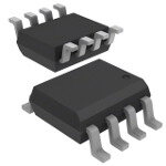
| 描述 | IC SUPERVISOR MPU 4.4V WD 8SOIC监控电路 5V CMOS MPU IC |
| 产品分类 | |
| 品牌 | Analog Devices |
| 产品手册 | |
| 产品图片 |
|
| rohs | 符合RoHS无铅 / 符合限制有害物质指令(RoHS)规范要求 |
| 产品系列 | 电源管理 IC,监控电路,Analog Devices ADM692AARNZ- |
| NumberofInputsMonitored | 1 Input |
| 数据手册 | |
| 产品型号 | ADM692AARNZ |
| 产品培训模块 | http://www.digikey.cn/PTM/IndividualPTM.page?site=cn&lang=zhs&ptm=25511 |
| 产品种类 | 监控电路 |
| 人工复位 | No Manual Reset |
| 供应商器件封装 | 8-SOIC |
| 功率失效检测 | Yes |
| 包装 | 管件 |
| 受监控电压数 | 1 |
| 商标 | Analog Devices |
| 复位 | 低有效 |
| 复位超时 | 最小为 140 ms |
| 安装类型 | 表面贴装 |
| 安装风格 | SMD/SMT |
| 封装 | Tube |
| 封装/外壳 | 8-SOIC(0.154",3.90mm 宽) |
| 封装/箱体 | SOIC-8 |
| 工作温度 | -40°C ~ 85°C |
| 工作电源电流 | 100 uA |
| 工厂包装数量 | 98 |
| 最大功率耗散 | 500 mW |
| 最大工作温度 | + 85 C |
| 最小工作温度 | - 40 C |
| 标准包装 | 98 |
| 欠电压阈值 | 4.25 V |
| 电压-阈值 | 4.4V |
| 电池备用开关 | Backup |
| 电源电压-最大 | 5.5 V |
| 电源电压-最小 | 4.5 V |
| 监视器 | Watchdog |
| 类型 | Voltage Supervisory |
| 系列 | ADM692A |
| 芯片启用信号 | No Chip Enable |
| 被监测输入数 | 1 Input |
| 输出 | 推挽式,图腾柱 |
| 输出类型 | Active High |
| 过电压阈值 | 4.5 V |
| 重置延迟时间 | 280 ms |
| 阈值电压 | 4.4 V |


- 商务部:美国ITC正式对集成电路等产品启动337调查
- 曝三星4nm工艺存在良率问题 高通将骁龙8 Gen1或转产台积电
- 太阳诱电将投资9.5亿元在常州建新厂生产MLCC 预计2023年完工
- 英特尔发布欧洲新工厂建设计划 深化IDM 2.0 战略
- 台积电先进制程称霸业界 有大客户加持明年业绩稳了
- 达到5530亿美元!SIA预计今年全球半导体销售额将创下新高
- 英特尔拟将自动驾驶子公司Mobileye上市 估值或超500亿美元
- 三星加码芯片和SET,合并消费电子和移动部门,撤换高东真等 CEO
- 三星电子宣布重大人事变动 还合并消费电子和移动部门
- 海关总署:前11个月进口集成电路产品价值2.52万亿元 增长14.8%


PDF Datasheet 数据手册内容提取
a Microprocessor Supervisory Circuits ADM690A/ADM692A/ADM802L/M/ADM805L/M FEATURES FUNCTIONAL BLOCK DIAGRAM Precision Supply Voltage Monitor 4.65 V ADM690A/ADM802L/ADM805L VBATT 4.40 V ADM692A/ADM802M/ADM805M Reset Assertion Down to 1 V VCC SWBIATTCTHEORVYER VOUT Reset Timeout—200 ms Watchdog Timer—1.6 s VCC 100 (cid:109)A Quiescent Supply Current RESET Automatic Battery Backup Power Switching 4.65V* GENERATOR RESET (RESET) Voltage Monitor for Power Fail (cid:54)2% Power Fail Accuracy on ADM802L/M ADM690A Space-Saving MicroSOIC Package (ADM690A) WINAPTUCTH (WDODGI) TRANSWITAIOTCNH DDEOTGECTOR ADM692A (1.6s) ADM802L APPLICATIONS ADM802M Microprocessor Systems ADM805L Computers POWER FAIL ADM805M INPUT (PFI) POWER FAIL Controllers 1.25V OUTPUT (PFO) Intelligent Instruments *4.4V FOR ADM692A/ADM802M/ADM805M ( ) = ADM805L/M ONLY GENERAL DESCRIPTION The ADM690A/ADM692A/ADM802L/M/ADM805L/M The ADM805L/M provides an active high reset output, RESET family of supervisory circuits offers complete single chip instead of RESET. solutions for power supply monitoring and battery control The family of products is fabricated using an advanced epitaxial functions in microprocessor systems. These functions include m P reset, backup battery switchover, watchdog timer, and power CMOS process combining low power consumption and high reliability. RESET assertion is guaranteed with V as low as 1 V. failure warning. CC They provide a pin-compatible upgrade for the MAX690A/ The ADM690A/ADM692A/ADM802L/M/ADM805L/M are MAX692A/MAX802L/MAX802M/MAX805L available in 8-pin packages and provide: 1. Power-on reset output during power-up, power-down and All parts are available in 8-pin DIP and SOIC packages. The brownout conditions. The RESET output remains opera- ADM690A is also available in a new space-saving microSOIC tional with V as low as 1 V. package. CC 2. Battery backup switching for CMOS RAM, CMOS microprocessor or other low power devices. 3. A reset pulse if the optional watchdog timer has not been toggled within 1.6 seconds. 4. A 1.25 V threshold detector for power fail warning, low battery detection, or to monitor a power supply other than +5 V. On the ADM690A/ADM802L/ADM805L the reset voltage threshold is 4.65 V. On the ADM692A/ADM802M/ ADM805M, the reset voltage threshold is 4.40 V. The ADM802L/ADM802M guarantee power fail accuracies to – 2%. REV.0 Information furnished by Analog Devices is believed to be accurate and reliable. However, no responsibility is assumed by Analog Devices for its use, nor for any infringements of patents or other rights of third parties One Technology Way, P.O. Box 9106, Norwood, MA 02062-9106, U.S.A. which may result from its use. No license is granted by implication or Tel: 617/329-4700 World Wide Web Site: http://www.analog.com otherwise under any patent or patent rights of Analog Devices. Fax: 617/326-8703 © Analog Devices, Inc., 1996
ADM690A/ADM692A/ADM802L/M/ADM805L/M–SPECIFICATIONS (V = 4.75 V to 5.5 V (ADM690A/ADM802L/ADM805L), V = 4.5 V to 5.5 V, (ADM692A/ADM802M/ADM805M), V = +2.8 V, T = T to T CC CC BATT A MIN MAX unless otherwise noted) Parameter Min Typ Max Units Test Conditions/Comments V /V OPERATION1 CC BATT V Operating Voltage Range 1.0 5.5 V CC Supply Current (Excludes I ) 70 100 m A OUT Supply Current in Battery Backup Mode 0.05 1.0 m A V = 0 V, V = 2.8 V CC BATT Battery Standby Current 5.5 V > V > V + 0.2 V CC BATT (+ = Discharge, – = Charge) –0.1 +0.02 m A V Output Voltage V – 0.02 V – 0.01 V I = 5 mA OUT CC CC OUT V – 0.5 V – 0.05 V I = 50 mA CC CC OUT V – 0.02 V I = 250 mA CC OUT V in Battery Backup Mode V – 0.05 V – 0.002 V I = 250 m A, V < V – 0.2 V OUT BATT BATT OUT CC BATT Battery Switchover Threshold 20 mV Power Up –20 mV Power Down Battery Switchover Hysteresis 40 mV RESET THRESHOLD Reset Voltage Threshold ADM690A, ADM802L, ADM805L 4.5 4.65 4.75 V ADM692A, ADM802M, ADM805M 4.25 4.4 4.5 V ADM802L 4.55 4.7 V T = 25(cid:176) C, V Falling A CC ADM802M 4.30 4.45 V T = 25(cid:176) C, V Falling A CC Reset Threshold Hysteresis 40 mV Reset Timeout Delay 140 200 280 ms RESET Output Voltage V – 1.5 V I = 800 m A CC SOURCE 0.4 V I = 3.2 mA SINK 0.3 V I = 100 m A, V = 1 V SINK CC RESET Output Voltage 0.8 V I = 4 m A, V = 1.1 V SOURCE CC V – 1.5 V ADM805L/M, I = 800 m A CC SOURCE 0.4 V ADM805L/M, I = 3.2 mA SINK WATCHDOG TIMER Watchdog Timeout Period 1.0 1.6 2.25 s WDI Input Pulse Width 50 ns V = 0.4, V = 0.8 (V ) IL IH CC WDI Input Threshold Logic Low 0.8 V Logic High 3.5 V WDI Input Current 10 m A WDI = V CC –10 m A WDI = 0 V POWER FAIL DETECTOR PFI Input Threshold 1.20 1.25 1.30 V ADM690A, ADM692A, ADM805L/M 1.225 1.25 1.275 V ADM802L/M PFI Input Current –25 0.01 +25 nA PFO Output Voltage V – 1.5 V I = 800 m A CC SOURCE 0.4 V I = 3.2 mA SINK NOTES 1Either V or V can be 0 V if the other > +2.0 V. CC BATT Specifications subject to change without notice. –2– REV. 0
ADM690A/ADM692A/ADM802L/M/ADM805L/M ABSOLUTE MAXIMUM RATINGS* ORDERING GUIDE (TA = +25(cid:176)C unless otherwise noted) Temperature Package V . . . . . . . . . . . . . . . . . . . . . . . . . . . . . . . . . –0.3 V to +6 V CC Model Range Option V . . . . . . . . . . . . . . . . . . . . . . . . . . . . . . . –0.3 V to +6 V BATT All Other Inputs . . . . . . . . . . . . . . . . . .–0.3 V to V + 0.3 V ADM690AAN –40(cid:176) C to +85(cid:176) C N-8 CC Input Current ADM690AARN –40(cid:176) C to +85(cid:176) C SO-8 V . . . . . . . . . . . . . . . . . . . . . . . . . . . . . . . . . . . . .200 mA ADM690AARM –40(cid:176) C to +85(cid:176) C RM-8 CC VBATT . . . . . . . . . . . . . . . . . . . . . . . . . . . . . . . . . . . 50 mA ADM692AAN –40(cid:176) C to +85(cid:176) C N-8 GND . . . . . . . . . . . . . . . . . . . . . . . . . . . . . . . . . . . . 20 mA ADM692AARN –40(cid:176) C to +85(cid:176) C SO-8 Digital Output Current . . . . . . . . . . . . . . . . . . . . . . . . 20 mA ADM802LAN –40(cid:176) C to +85(cid:176) C N-8 Power Dissipation, N-8 DIP . . . . . . . . . . . . . . . . . . . 400 mW ADM802LARN –40(cid:176) C to +85(cid:176) C SO-8 q Thermal Impedance . . . . . . . . . . . . . . . . . . . . 120(cid:176) C/W PowJAer Dissipation, SO-8 SOIC . . . . . . . . . . . . . . . . . 500 mW ADM802MAN –40(cid:176) C to +85(cid:176) C N-8 q Thermal Impedance . . . . . . . . . . . . . . . . . . . . 110(cid:176) C/W ADM802MARN –40(cid:176) C to +85(cid:176) C SO-8 JA Operating Temperature Range ADM805LAN –40(cid:176) C to +85(cid:176) C N-8 Industrial (A Version) . . . . . . . . . . . . . . . . –40(cid:176) C to +85(cid:176) C ADM805LARN –40(cid:176) C to +85(cid:176) C SO-8 Lead Temperature (Soldering, 10 sec) . . . . . . . . . . . .+300(cid:176) C ADM805MAN –40(cid:176) C to +85(cid:176) C N-8 Vapor Phase (60 sec) . . . . . . . . . . . . . . . . . . . . . . . .+215(cid:176) C ADM805MARN –40(cid:176) C to +85(cid:176) C SO-8 Infrared (15 sec) . . . . . . . . . . . . . . . . . . . . . . . . . . . .+220(cid:176) C Storage Temperature Range . . . . . . . . . . . . –65(cid:176) C to +150(cid:176) C PIN CONFIGURATIONS ESD Rating . . . . . . . . . . . . . . . . . . . . . . . . . . . . . . . . . .>4 kV *Spterremssaense natb odvaem tahgoes et ol itshteed duevnidceer. T“Ahibss oisl uate stMreassx imrautimng Roantliyn gasn”d mfuanyc tciaounsael VOUT 1 AADDMM669902AA 8 VBATT operation of the device at these or any other conditions above those listed in the VCC 2 AADDMM880022ML 7 RESET (RESET) operational sections of this specification is not implied. Exposure to absolute GND 3 ADM805L 6 WDI ADM805M maximum ratings for extended periods of time may affect device reliability. PFI 4 TOP VIEW 5 PFO (Not to Scale) PIN FUNCTION DESCRIPTION Mnemonic Function V Power Supply Input: +5 V Nominal. CC V Backup Battery Input. As V falls below the reset threshold and below V by 20 mV, V will be switched BATT CC BATT BATT to V . On power-up as V rises to 20 mV above V , V will be switched back to V . OUT CC BATT OUT CC V Output Voltage. When V is above the reset threshold, V is connected to V through an on chip switch. OUT CC OUT CC When V is below the reset threshold, the higher of V or V is connected to V . CC CC BATT OUT GND 0 V. Ground reference for all signals. PFI Power Fail Comparator Input. If PFI is less than 1.25 V, the power fail output PFO goes low. If unused, PFI should be connected to V or GND. CC PFO Power Fail Comparator Output. If PFI is less than 1.25 V, the power fail output PFO goes low. RESET Logic Output. RESET goes low if 1. V falls below the Reset Threshold CC 2. The watchdog timer is not serviced within its timeout period (1.6 seconds) The reset threshold is typically 4.65 V for the ADM690A/ADM802L/ADM805L and 4.4 V for the ADM692A/ ADM802M/ADM805M. RESET remains low for 200 ms after V returns above the threshold. RESET also CC goes low for 200 ms if the watchdog timer is enabled but not serviced within its timeout period. RESET Active high RESET output (ADM805L/M only). This is the inverse of RESET. The asserted (high) level is V CC or V whichever is higher. BATT WDI Watchdog Input. WDI is a three level input. If WDI remains either high or low for longer than 1.6 s, (RESET) (RESET) is activated. The timer resets with each transition on the WDI line. The watchdog timer may be disabled if WDI is left floating or is connected to a high impedance three stated logic output. REV. 0 –3–
ADM690A/ADM692A/ADM802L/M/ADM805L/M Typical Performance Curves 3 5.00 4.98 2.75 4.96 ROUT = 9.3W 4.88 ROUT = 0.53W V – VOUT 2.5 V – VOUT4.92 4.9 2.25 4.88 4.86 2 4.84 10 20 30 40 50 60 70 20 50 100 150 200 IOUT – mA IOUT – mA Figure 1.Output Voltage vs. Load Current in Battery Figure 4.Output Voltage vs. Load Current in Normal Backup Operation TA = +25(cid:56)C 5V 100 100 90 90 PFO PFO 1.3V 10 10 0V 0% 0% PFI 1.3V 1.2V 200mV 2µs PFI 200mV 2µs 1.2V Figure 2.Power Fail Comparator Response Time L (cid:221) H Figure 5.Power Fail Comparator Response Time H (cid:221) L TA = +25(cid:56)C 5V 100 100 VCC 90 4V 90 RESET 10 10 0% 0% 1V 10µs 1V 400ms Figure 3.ADM690A RESET Response Time Figure 6.RESET Output Voltage vs. VCC –4– REV. 0
ADM690A/ADM692A/ADM802L/M/ADM805L/M +5V VBATT VCC SWBIATTCTHEORVYER VOUT 0V VCC VOUT 3.0V tRS RESET 0V 4.65V* GENERATOR RESET +5V (RESET) RESET ADM690A WATCHDOG WATCHDOG ADM692A 0V INPUT (WDI) TRANSITION DETECTOR +5V (1.6s) ADM802L RESET ADM802M 3.0V ADM805L 0V POWER FAIL ADM805M INPUT (PFI) POWER FAIL +5V 1.25V OUTPUT (PFO) PFO VBATT = PFI = 3.0V 0V *4.4V FOR ADM692A/ADM802M/ADM805M ( ) = ADM805L/M ONLY Figure 7.Functional Block Diagram Figure 8.Timing Diagram POWER FAIL RESET, RESET BATTERY SWITCHOVER SECTION RESET is an active low output which provides a RESET signal During normal operation with V higher than the reset CC to the microprocessor whenever V is at an invalid level. When threshold, V is internally switched to V via an internal CC CC OUT V falls below the reset threshold, the RESET output is forced PMOS transistor switch. This switch has a typical on-resistance CC low. The nominal reset voltage threshold is 4.65 V (ADM690A/ of less than 1 W and can supply up to 100 mA at the V OUT ADM802L/ADM805L or 4.4 V ADM692A/ADM802M/ terminal. Once V falls below the reset threshold, the higher of CC ADM805M. V or V is switched to V . This means that V CC BATT OUT BATT On power-up RESET will remain low for 200 ms after V rises connects to VOUT only when VCC is below the reset threshold CC above the reset threshold. This allows time for the power supply and VBATT is greater than VCC. and microprocessor to stabilize. On power-down, the RESET V is normally used to drive a RAM memory bank which OUT output remains low with V as low as 1 V. This ensures that may require instantaneous currents of greater than 100 mA. If CC the microprocessor is held in a stable shutdown condition. this is the case, then a bypass capacitor should be connected to The guaranteed minimum and maximum thresholds are as follows: VOUT. The capacitor will provide the peak current transients to the ADM690A/ADM802L/ADM805L: 4.5 V and 4.75 V RAM. A capacitance value of 0.1m F or greater may be used. ADM692A: 4.25 V and 4.5 V. A 9 W MOSFET switch connects the V input to V BATT OUT ADM802L: 4.55 V and 4.7 V during battery backup. This MOSFET has very low input-to- output differential (dropout voltage) at the low current levels ADM802M: 4.3 V and 4.45 V required for battery backup of CMOS RAM or other low power The ADM805L and ADM805M contain an active high reset CMOS circuitry. The supply current in battery backup is output. This is the complement of RESET and is intended for typically 0.05 m A. processors requiring an active high RESET signal. Typically 3 V batteries are used as the backup supply. High The guaranteed minimum and maximum thresholds for the value capacitors, either standard electrolytic or the farad size ADM805 are: double layer capacitors, can also be used for short-term memory ADM805L: 4.5 V and 4.75 V back up. A small charging current of typically 10 nA (0.1 m A ADM805M: 4.25 V and 4.5 V. max) flows out of the V terminal. This current is useful for BATT maintaining rechargeable batteries in a fully charged condition. Watchdog Timer RESET, RESET This extends the life of the back up battery by compensating for The watchdog timer circuit monitors the activity of the micro- its self discharge current. Also note that this current poses no processor in order to check that it is not stalled in an indefinite problem when lithium batteries are used for back up since the loop. An output line on the processor is used to toggle the maximum charging current (0.1 m A) is safe for even the smallest Watchdog Input (WDI) line. If this line is not toggled within lithium cells. 1.6 seconds, a RESET pulse is generated. The watchdog timeout period restarts with each transition on the WDI pin. To If the battery-switchover section is not used, V should be BATT ensure that the watchdog timer does not time out, either a connected to GND and V should be connected to V . OUT CC high-to-low or low-to-high transition on the WDI pin must occur at or less than the minimum timeout period. If WDI remains permanently either high or low, reset pulses will be issued after each timeout period (1.6 s). The watchdog monitor can be deactivated by floating the Watchdog Input (WDI) or by connecting it to midsupply. REV. 0 –5–
ADM690A/ADM692A/ADM802L/M/ADM805L/M Table I. Input and Output Status in Battery Backup Mode INPUT POWER Signal Status TO R1 1.25V (PFO) µP NMI V V is connected to V via an internal OUT OUT BATT PFI PMOS switch. R2 RESET Logic low. R3 RESET Logic high (ADM805L, ADM805M). The open circuit output voltage is equal to V . OUT PFI The power fail comparator is disabled 5V PFO Logic low. WDI The watchdog timer is disabled PFO Power Fail Comparator The power fail comparator is an independent comparator 0V that may be used to monitor the input power supply. The 0V VL VH comparator’s inverting input is internally connected to a 1.25 VIN V reference voltage. The noninverting input is available at the PFI input. This input may be used to monitor the input power R2+R3 supply via a resistive divider network. When the voltage on the VH = 1.25 1+ R 2 · R 3 R1 PFI input drops below 1.25 V, the comparator output (PFO) goes low indicating a power failure. For early warning of power VL = 1.25+R1 1.R225 – V C CR–31.25 failure the comparator may be used to monitor the preregulator input simply by choosing an appropriate resistive divider R1+R2 network. The PFO output can be used to interrupt the VMID= 1.25 R2 processor so that a shutdown procedure is implemented before the power is lost. Figure 10. Adding Hysteresis to the Power Fail Comparator INPUT POWER TYPICAL APPLICATIONS R1 1.25V (PFO) POWER FAIL Figure 11 shows a typical power monitoring, battery backup OUTPUT application. V powers the CMOS RAM. Under normal OUT POWER operating conditions with V present, V is internally R2 FAIL CC OUT INPUT connected to V . If a power failure occurs, V will decay and CC CC V will be switched to V thereby maintaining power for OUT BATT the CMOS RAM. A RESET pulse is also generated when V CC Figure 9.Power Fail Comparator falls below the reset threshold. Adding Hysteresis to the Power Fail Comparator For increased noise immunity, hysteresis may be added to the UNREGDUCLATED +5V power fail comparator. Since the comparator circuit is non- VCC µP POWER inverting, hysteresis can be added simply by connecting a R1 resistor between the PFO output and the PFI input as shown in VOUT CPOMWOSE RRAM PFI Figure 10. When PFO is low, resistor R3 sinks current from the summing junction at the PFI pin. When PFO is high, resistor R2 µP SYSTEM R3 sources current into the PFI summing junction. This results VBATT RESET µP RESET in differing trip levels for the comparator. Further noise PFO µP NMI + immunity may be achieved by connecting a capacitor between BATTERY GND WDI I/O LINE PFI and GND. Figure 11.Typical Application Circuit The watchdog timer input (WDI) monitors an I/O line from the m P system. This line must be toggled once every 1.6 seconds to verify correct software execution. Failure to toggle the line indicates that the m P system is not correctly executing its program and may be tied up in an endless loop. If this happens, a reset pulse is generated to initialize the processor. –6– REV. 0
ADM690A/ADM692A/ADM802L/M/ADM805L/M If the watchdog timer is not needed, the WDI input should be Operation Without a Backup Supply left floating. If a backup power source is not used, V should be con- BATT nected to GND and V should be connected to V . The Power Fail Input, PFI, monitors the input power supply via OUT CC a resistive divider network. The voltage on the PFI input is Replacing the Backup Battery compared with a precision 1.25 V internal reference. If the input The backup battery may be replaced without any danger of voltage drops below 1.25 V, a power fail output (PFO) signal is spurious resetting when V is present. Since V is above the CC CC generated. This warns of an impending power failure and may reset threshold, a reset will not occur even if V is floating BATT be used to interrupt the processor so that the system may be while a replacement battery is being inserted. This differs from shut down in an orderly fashion. The resistors in the sensing older generation products where leakage currents flowing out network are ratioed to give the desired power fail threshold V could cause spurious resetting during battery replacement. BATT voltage VT. (cid:109)Ps With Bidirectional RESET V = (1.25 R1/R2) + 1.25 V In order to prevent contention for microprocessors with a T bidirectional reset line, a current limiting resistor should be R1/R2 = (V /1.25) – 1 T inserted between the ADM69xA/ADM80xx RESET output pin Alternate Watchdog Input Drive Circuits and the m P reset pin. This will limit the current to a safe level if The watchdog feature can be enabled and disabled under there are conflicting output reset levels. A suitable resistor value program control by driving WDI with a 3-state buffer. When is 4.7 kW . If the reset output is required for other uses, then it three-stated, the WDI input will float thereby disabling the should be buffered as shown in Figure 13. watchdog timer. BUFFERED High Capacity Backup Capacitors RESET High capacity (0.1 m F or greater) capacitors may be used as a +5V backup power source. A typical application is shown in Fig- ure 12. VCC ADM690A +5V ADM692A ADM802L ADM802M µP VCC VOUT TO STATIC RAM RESET RESET GND GND VBATT RREESSEETT* TO µP + 0.1F GND Figure 13.Bidirectional Reset *FOR ADM805L/ADM805M ONLY Figure 12.High Capacity Capacitor REV. 0 –7–
ADM690A/ADM692A/ADM802L/M/ADM805L/M OUTLINE DIMENSIONS Dimensions shown in inches and (mm). 8-Pin Plastic DIP (N-8) 6 9 0.430 (10.92) 0/ 0.348 (8.84) –1 2 1 8 5 – 0.280 (7.11) 7 9 0.240 (6.10) 1 1 4 0.325 (8.25) C2 PIN 1 0.060 (1.52) 0.300 (7.62) 0.210 (5.33) 0.015 (0.38) 0.195 (4.95) MAX 0.130 0.115 (2.93) 0.160 (4.06) (3.30) 0.115 (2.93) MIN 0.015 (0.381) 00..002124 ((00..535586)) (02.1.5040) 00..007405 ((11..7175)) SPELAANTIENG 0.008 (0.204) BSC 8-Lead SOIC (SO-8) 0.1968 (5.00) 0.1890 (4.80) 8 5 0.1574 (4.00) 0.2440 (6.20) 0.1497 (3.80) 1 4 0.2284 (5.80) PIN 1 0.0688 (1.75) 0.0196 (0.50)x 45(cid:176) 0.0098 (0.25) 0.0532 (1.35) 0.0099 (0.25) 0.0040 (0.10) 8(cid:176) SEPALTAINNGE 0(B1.0.S25C70)0 00..00119328 ((00..4395)) 00..00009785 ((00..2159)) 0(cid:176) 00..00510600 ((10..2471)) 8-Lead MicroSOIC (RM-8) 0.122 (3.10) 0.114 (2.90) 8 5 0.122 (3.10) 0.199 (5.05) 0.114 (2.90) 0.187 (4.75) 1 4 A. S. PIN 1 U. 0.0256 (0.65) BSC N 0.120 (3.05) 0.120 (3.05) D I 0.112 (2.84) 0.112 (2.84) TE 0.043 (1.09) N 0.006 (0.15) 0.037 (0.938) RI 0.002 (0.05) 33(cid:176) P SEATING 00..001088 ((00..4260)) 0.011 (0.28) 27(cid:176) 0.027 (0.68) PLANE 0.003 (0.08) 0.015 (0.38) –8– REV. 0