ICGOO在线商城 > 集成电路(IC) > PMIC - 监控器 > ADM691AARWZ-REEL
 Datasheet下载
- 型号: ADM691AARWZ-REEL
- 制造商: Analog
- 库位|库存: xxxx|xxxx
- 要求:
| 数量阶梯 | 香港交货 | 国内含税 |
| +xxxx | $xxxx | ¥xxxx |
查看当月历史价格
查看今年历史价格
ADM691AARWZ-REEL产品简介:
ICGOO电子元器件商城为您提供ADM691AARWZ-REEL由Analog设计生产,在icgoo商城现货销售,并且可以通过原厂、代理商等渠道进行代购。 ADM691AARWZ-REEL价格参考。AnalogADM691AARWZ-REEL封装/规格:PMIC - 监控器, 开路漏极,推挽式 监控器 1 通道 16-SOIC。您可以下载ADM691AARWZ-REEL参考资料、Datasheet数据手册功能说明书,资料中有ADM691AARWZ-REEL 详细功能的应用电路图电压和使用方法及教程。
ADM691AARWZ-REEL 是由 Analog Devices Inc. 生产的一款电源管理集成电路(PMIC),属于监控器类别。该器件主要应用于需要对电源电压进行监控、复位控制和看门狗定时器功能的电子系统中。

典型应用场景包括:

1. 嵌入式系统与工业控制:用于监控系统电源电压,当电压低于设定阈值时触发复位信号,确保微处理器或微控制器在异常情况下可靠复位,防止系统运行异常。

2. 通信设备:在通信模块或基站设备中,用于监控供电电压的稳定性,保障系统长时间运行的可靠性。

3. 消费电子产品:如机顶盒、家用智能控制器等,提供电源监控和看门狗功能,防止程序跑飞或系统死机。

4. 汽车电子系统:用于车载控制系统中,监控电源状态并提供复位功能,确保车辆电子模块在电压异常后能自动恢复正常运行。

5. 数据采集与测量设备:在高精度测量系统中,确保系统在电源异常时及时复位,避免数据丢失或误操作。

该芯片采用16引脚TSSOP封装,具备低功耗特性,适用于宽电压范围(通常支持5V系统),集成复位输出、看门狗定时器和电压监控功能,是一款高集成度、高可靠性的电源监控解决方案。
| 参数 | 数值 |
| 产品目录 | 集成电路 (IC) |
| 描述 | IC SUPERVISOR MPU 4.65V 16SOIC |
| 产品分类 | |
| 品牌 | Analog Devices Inc |
| 数据手册 | |
| 产品图片 |
|
| 产品型号 | ADM691AARWZ-REEL |
| rohs | 无铅 / 符合限制有害物质指令(RoHS)规范要求 |
| 产品系列 | - |
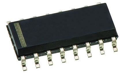
| 供应商器件封装 | 16-SOIC W |
| 其它名称 | ADM691AARWZ-REELDKR |
| 包装 | Digi-Reel® |
| 受监控电压数 | 1 |
| 复位 | 高有效/低有效 |
| 复位超时 | 最小为 140 ms |
| 安装类型 | 表面贴装 |
| 封装/外壳 | 16-SOIC(0.295",7.50mm 宽) |
| 工作温度 | -40°C ~ 85°C |
| 标准包装 | 1 |
| 电压-阈值 | 4.65V |
| 类型 | 备用电池电路 |
| 输出 | 开路漏极,推挽式 |


PDF Datasheet 数据手册内容提取
a Microprocessor Supervisory Circuits ADM691A/ADM693A/ADM800L/M FEATURES FUNCTIONAL BLOCK DIAGRAM Low Power Consumption: Precision Voltage Monitor BATT ON (cid:54)2% Tolerance on ADM800L/M 4.65V1 Reset Time Delay—200 ms, or Adjustable LOW LINE 1 (cid:109)A Standby Current VCC Automatic Battery Backup Power Switching Fast Onboard Gating of Chip Enable Signals VOUT Also Available in TSSOP Package (ADM691A) VBATT APPLICATIONS CHIP ENABLE OUTPUT Microprocessor Systems CONTROL Computers CEIN CEOUT Controllers Intelligent Instruments Automotive Systems OSOCS CS EINL WTRAIMETESCBEHTAD S&OEG GERNEESREATT &OR RESET Critical (cid:109)P Power Monitoring RESET WATCHDOG WATCHDOG WATCHDOG WATCHDOG INPUT (WDI) TRANSITION DETECTOR TIMER OUTPUT (WDO) GENERAL DESCRIPTION POWER FAIL INPUT (PFI) POWER FAIL The ADM691A/ADM693A/ADM800L/ADM800M family of 1.25V OUTPUT (PFO) ADM691A/ADM693A supervisory circuits offers complete single chip solutions for ADM800L/ADM800M power supply monitoring and battery control functions in microprocessor systems. These functions include m P reset, 1VOLTAGE DETECTOR = 4.4V (ADM693A/ADM800M) backup-battery switchover, watchdog timer, CMOS RAM write protection, and power-failure warning. The family of products provides an upgrade for the MAX691A/93A/800M family of products. INPUT POWER All parts are available in 16-pin DIP and SO packages. The 7805 +5V 0.1µF ADM691A is also available in a space-saving TSSOP package. VCC The following functionality is provided: CMOS RAM 1. Power-on reset output during power-up, power-down and VCC BAT VOUT brownout conditions. The circuitry remains operational with R1 BATTERY VBATT ON CEOUT ADDEDCROEDSES VCC as low as 1 V. AADDMM669913AA CEIN A0–A15 µP 2. Battery backup switching for CMOS RAM, CMOS micro- PFI ADM800L POWER ADM800M processor or other low power logic. GND WDI I/O LINE R2 OSC IN PFO NMI µP 3. A reset pulse if the optional watchdog timer has not been NC OSC SEL RESET RESET toggled within a specified time. LOW LINE WDO 4. A 1.25 V threshold detector for power fail warning, low bat- tery detection, or to monitor a power supply other than +5 V. SYSTEM STATUS INDICATORS Figure 1.Typical Application REV.0 Information furnished by Analog Devices is believed to be accurate and reliable. However, no responsibility is assumed by Analog Devices for its use, nor for any infringements of patents or other rights of third parties One Technology Way, P.O. Box 9106, Norwood, MA 02062-9106, U.S.A. which may result from its use. No license is granted by implication or Tel: 617/329-4700 World Wide Web Site: http://www.analog.com otherwise under any patent or patent rights of Analog Devices. Fax: 617/326-8703 © Analog Devices, Inc., 1996
ADM691A/ADM693A/ADM800L/M–SPECIFICATIONS (V = 4.75 V to 5.5 V (ADM691A, ADM800L) 4.5 V to 5.5 V (ADM693A, ADM800M) V = +2.8 V, T = T to T unless otherwise noted) CC BATT A MIN MAX Parameter Min Typ Max Unit Test Conditions/Comments BATTERY BACKUP SWITCHING V , V Operating Voltage Range 0 5.5 V CC BATT V Output Voltage V – 0.05 V – 0.02 V I = 25 mA OUT CC CC OUT V – 0.3 V – 0.2 V I = 250 mA CC CC OUT V to V Output Resistance 0.8 1.2 W V = 4.5 V CC OUT CC V in Battery Backup Mode V – 0.3 V V = 4.5 V, I = 20 mA OUT BATT BATT OUT V – 0.25 V V = 2.8 V, I = 10 mA BATT BATT OUT V – 0.15 V V = 2.0 V, I = 5 mA BATT BATT OUT V to V Output Resistance 12 W V = 4.5 V BATT OUT BATT 20 W V = 2.8 V BATT 25 W V = 2.0 V BATT Supply Current (Excludes I ) 70 100 m A V > (V – 1 V) OUT CC BATT Supply Current in B. Backup (Excludes I ) 0.04 1 m A V < (V – 1.2 V), V = 2.8 V OUT CC BATT BATT Battery Standby Current 5.5 V > V > V + 0.2 V CC BATT (+ = Discharge, – = Charge) –0.1 +0.02 m A (V +0.2 V) < V , T = +25(cid:176) C BATT CC A –1.0 +0.02 m A (V +0.2 V) < V BATT CC Battery Switchover Threshold V + 0.03 V Power Up BATT V –V V – 0.03 V Power Down CC BATT BATT Battery Switchover Hysteresis 60 mV BATT ON Output Voltage Low 0.1 0.4 V I = 3.2 mA SINK 0.7 1.5 V I = 25 mA SINK BATT ON Output Short Circuit Current 60 mA Sink Current 1 15 100 m A Source Current RESET AND WATCHDOG TIMER Reset Voltage Threshold ADM691A, ADM800L 4.5 4.65 4.75 V ADM693A, ADM800M 4.25 4.40 4.50 V ADM800L, V Falling 4.55 4.70 V T = +25(cid:176) C CC A ADM800M, V Falling 4.3 4.45 V T = +25(cid:176) C CC A Reset Threshold Hysteresis 15 mV V to RESET Delay 80 m s Power Down CC LOW LINE to RESET Delay 800 ns Reset Timeout Period Internal Oscillator 140 200 280 ms Power Up Reset Timeout Period External Clock 2048 Cycles Power Up Watchdog Timeout Period, Internal Oscillator 1.0 1.6 2.25 s Long Period 70 100 140 ms Short Period Watchdog Timeout Period, External Clock 4096 Cycles Long Period 1024 Cycles Short Period Minimum WDI Input Pulse Width 100 ns V = 0.4, V = 0.75 · V IL IH CC RESET Output Voltage 0.004 0.3 V I = 50 m A, V = 1 V, V = 0 V SINK CC BATT 0.1 0.4 V I = 3.2 mA, V = 4.25 V SINK CC 3.5 V I = 1.6 mA, V = 5 V SOURCE CC RESET Output Short Circuit Current 7 20 mA RESET Output Voltage Low 0.1 0.4 V I = 3.2 mA SINK LOW LINE Output Voltage 0.4 V I = 3.2 mA, V = 4.25 V SINK CC 3.5 V I = 1 m A, V = 5 V SOURCE CC LOW LINE Short Circuit Source Current 1 15 100 m A WDO Output Voltage 0.4 V I = 3.2 mA, V = 4.25 V SINK CC 3.5 V I = 500 m A, V = 5 V SOURCE CC WDO Short Circuit Source Current 3 10 mA WDI Input Threshold Logic Low 0.8 V Logic High 0.75 · V V CC WDI Input Current –50 –10 m A WDI = 0 V 20 50 m A WDI = V OUT POWER FAIL DETECTOR PFI Input Threshold ADM69xA 1.2 1.25 1.3 V V = 5 V CC PFI Input Threshold ADM800L/M 1.225 1.25 1.275 V V = 5 V CC PFI Input Current – 0.01 – 25 nA PFO Output Voltage 0.4 V I = 3.2 mA SINK 3.5 I = 1 m A SOURCE PFO Short Circuit Source Current 1 15 100 m A PFI to PFO Delay 25 m s V = –20 mV IN 60 m s V = 20 mV IN –2– REV. 0
ADM691A/ADM693A/ADM800L/M Parameter Min Typ Max Units Test Conditions/Comments CHIP ENABLE GATING CE Leakage Current – 0.005 – 1 m A Disable Mode IN CE to CE Resistance 40 150 W Enable Mode IN OUT CE to CE Propagation Delay 6 10 ns R = 50 W , C = 50 pF IN OUT IN LOAD CE Short-Circuit Current 0.1 0.75 2.0 mA Disable Mode, CE = 0 V OUT OUT CE Output Voltage 3.5 V V = 5 V, I = –100 m A OUT CC OUT 2.7 V V = 0 V, V = 2.8 V, I = 1 m A CC BATT OUT RESET to CE Propagation Delay 12 m s Power Down OUT OSCILLATOR OSC IN Input Current 0.1 – 5 m A OSC SEL = 0 V OSC In Input Pullup Current 10 100 m A OSC SEL = V or Floating OUT OSC SEL Input Pullup Current 10 100 m A OSC SEL = 0 V OSC IN Frequency Range 500 kHz OSC SEL = 0 V OSC IN Threshold Voltage V – 0.4 V – 0.6 V V OUT OUT IH 3.65 2.00 V V IL OSC IN Frequency with Ext Capacitor 100 kHz OSC SEL = 0 V, C = 47 pF OSC NOTES 1Either V or V can be 0 V if the other > +2.0 V. CC BATT Specifications subject to change without notice. ABSOLUTE MAXIMUM RATINGS* ORDERING GUIDE (T = 25(cid:176)C unless otherwise noted) A V . . . . . . . . . . . . . . . . . . . . . . . . . . . . . . . . . –0.3 V to +6 V Temperature Package CC V . . . . . . . . . . . . . . . . . . . . . . . . . . . . . . . –0.3 V to +6 V Model Range Option BATT All Other Inputs . . . . . . . . . . . . . . . . .–0.3 V to V + 0.5 V OUT ADM691AAN –40(cid:176) C to +85(cid:176) C N-16 Input Current ADM691AARN –40(cid:176) C to +85(cid:176) C R-16N V (Peak) . . . . . . . . . . . . . . . . . . . . . . . . . . . . . . .1000 mA CC ADM691AARW –40(cid:176) C to +85(cid:176) C R-16W V (Continuous) . . . . . . . . . . . . . . . . . . . . . . . . . . .250 mA CC ADM691AARU –40(cid:176) C to +85(cid:176) C RU-16 V (Peak) . . . . . . . . . . . . . . . . . . . . . . . . . . . . . .250 mA BATT ADM693AAN –40(cid:176) C to +85(cid:176) C N-16 V (Continuous) . . . . . . . . . . . . . . . . . . . . . . . . . .25 mA BATT ADM693AARN –40(cid:176) C to +85(cid:176) C R-16N GND, BATT ON . . . . . . . . . . . . . . . . . . . . . . . . . . . .100 mA ADM693AARW –40(cid:176) C to +85(cid:176) C R-16W Digital Output Current . . . . . . . . . . . . . . . . . . . . . . . . .25 mA Power Dissipation, N-16 DIP . . . . . . . . . . . . . . . . . . 842 mW ADM800LAN –40(cid:176) C to +85(cid:176) C N-16 q J A Thermal Impedance . . . . . . . . . . . . . . . . . . . . .135(cid:176) C/W ADM800LARN –40(cid:176) C to +85(cid:176) C R-16N Power Dissipation, R-16 Narrow SOIC . . . . . . . . . . . 700 mW ADM800LARW –40(cid:176) C to +85(cid:176) C R-16W q Thermal Impedance . . . . . . . . . . . . . . . . . . . . . . .110(cid:176) W ADM800MAN –40(cid:176) C to +85(cid:176) C N-16 JA Power Dissipation, R-16 Wide SOIC . . . . . . . . . . . . . 762 mW ADM800MARN –40(cid:176) C to +85(cid:176) C R-16N q Thermal Impedance . . . . . . . . . . . . . . . . . . . . .110(cid:176) C/W ADM800MARW –40(cid:176) C to +85(cid:176) C R-16W JA Power Dissipation, RU-16 TSSOP . . . . . . . . . . . . . . 500 mW q Thermal Impedance . . . . . . . . . . . . . . . . . . . . .158(cid:176) C/W JA Operating Temperature Range Industrial (A Version) . . . . . . . . . . . . . . . . –40(cid:176) C to +85(cid:176) C Lead Temperature (Soldering, 10 sec) . . . . . . . . . . . .+300(cid:176) C Vapor Phase (60 sec) . . . . . . . . . . . . . . . . . . . . . . . . .215(cid:176) C Infrared (15 sec) . . . . . . . . . . . . . . . . . . . . . . . . . . . .+220(cid:176) C Storage Temperature Range . . . . . . . . . . . . –65(cid:176) C to +150(cid:176) C *Stresses above those listed under “Absolute Maximum Ratings” may cause perma- nent damage to the device. This is a stress rating only and functional operation of the device at these or any other conditions above those listed in the operational sections of this specification is not implied. Exposure to absolute maximum ratings for extended periods of time may affect device reliability. Table I. Product Selection Table Power On Low V Watchdog Battery Backup Base Drive Chip Enable CC Part No. Reset Time Threshold Timeout Switching Ext PNP Signals ADM691A 200 ms or Adj. 4.65 V – 3% 100 ms, 1.6 s, Adj. Yes Yes Yes ADM693A 200 ms or Adj. 4.4 V – 3% 100 ms, 1.6 s, Adj. Yes Yes Yes ADM800M 200 ms or Adj. 4.4 V – 2% 100 ms, 1.6 s, Adj. Yes Yes Yes ADM800L 200 ms or Adj. 4.65 V – 2% 100 ms, 1.6 s, Adj. Yes Yes Yes REV. 0 –3–
ADM691A/ADM693A/ADM800L/M PIN DESCRIPTIONS Pin Mnemonic Function 1 V Backup Battery Input. Connect to external battery or capacitor. Connect to ground if a backup battery is BATT not used. 2 V Output Voltage, V or V is internally switched to V depending on which is at the highest poten- OUT CC BATT OUT tial. When V is higher than V and is also higher than the reset threshold, V is switched to V . CC BATT CC OUT When V is lower than V and below the reset threshold, V is switched to V . Connect V to CC BATT BATT OUT OUT V if a backup battery is not being used. CC 3 V Power Supply Input; +5 V. CC 4 GND 0 V. Ground reference for all signals. 5 BATT ON Logic Output. BATT ON goes high when V is internally switched to the V input. It goes low when OUT BATT V is internally switched to V . The output may also be used to drive the base (via a resistor) of an ex- OUT CC ternal PNP transistor to increase the output current above the 250 mA rating of V . OUT 6 LOW LINE Logic Output. LOW LINE goes low when V falls below the reset threshold. It returns high as soon as CC V rises above the reset threshold. CC 7 OSCIN Oscillator Logic Input. With OSC SEL high or floating, the internal oscillator is enabled and sets the reset delay and the watchdog timeout period. Connecting OSCIN low selects 100 ms while leaving it floating selects 1.6 sec. With OSC SEL low, OSC IN can be driven by an external clock signal or an external ca- pacitor can be connected between OSC IN and GND. This sets both the reset active pulse timing and the watchdog timeout period. (See Table II and Figure 4.) 8 OSC SEL Logic Oscillator Select Input. When OSC SEL is unconnected (floating) or driven high, the internal oscil- lator sets the reset active time and watchdog timeout period. When OSC SEL is low, the external oscillator input, OSCIN, is enabled. OSC SEL has a 10 m A internal pullup. 9 PFI Power Fail Input. PFI is the noninverting input to the Power Fail Comparator. When PFI is less than 1.25 V, PFO goes low. Connect PFI to GND or V when not used. OUT 10 PFO Power Fail Output. PFO is the output of the Power Fail Comparator. It goes low when PFI is less than 1.25 V. 11 WDI Watchdog Input. WDI is a three level input. If WDI remains either high or low for longer than the watch- dog timeout period, RESET pulses low and WDO goes low. The timer resets with each transition on the WDI line. The Watchdog Timer may be disabled if WDI is left floating or is driven to midsupply. 12 CE Output. CE goes low only when CE is low and V is above the reset threshold. If CE is low when OUT OUT IN CC IN reset is asserted, CE will remain low for 15 m s or until CE goes high, whichever occurs first. OUT IN 13 CE Chip Enable Input. The input to the CE gating circuit. Connect to GND or V if not used. IN OUT 14 WDO Logic Output. The Watchdog Output, WDO, goes low if WDI remains either high or low for longer than the Watchdog timeout period. WDO is set high by the next transition at WDI. WDO remains high if WDI is unconnected. 15 RESET Logic Output. RESET goes low if V falls below the Reset Threshold. It remains low for 200 ms typ after CC V goes above the reset threshold. CC 16 RESET Logic Output. RESET is an open-drain output. It is the inverse of RESET. PIN CONFIGURATIONS VBATT 1 16 RESET VOUT 2 15 RESET VCC 3 ADM691A 14 WDO ADM693A GND 4 ADM800L 13 CEIN BATT ON 5 ADM800M 12 CEOUT LOW LINE 6 11 WDI TOP VIEW OSC IN 7 (Not to Scale) 10 PFO OSC SEL 8 9 PFI –4– REV. 0
Typical Performance Curves–ADM691A/ADM693A/ADM800L/M 100 1.2 90 R1.1 – – µA 80 NCE T A1.0 REN 70 SIST R E Y CU 60 ON R0.9 UPPL 50 VOUT 0.8 V SCC 40 TO CC V0.7 30 20 0.6 –50 –25 0 25 50 75 100 125 –50 –30 –10 10 30 50 70 90 TEMPERATURE – (cid:176)C TEMPERATURE – (cid:176)C Figure 2.I vs. Temperature: Normal Operation Figure 5.V to V ON-Resistance vs. Temperature CC CC OUT 60 80 70 A 55 n Y SUPPLY CURRENT – 445500 V TO V – mVCCOUT43650000 ROUT = 0.67W R TE 20 T A B 35 10 30 0 –50 –30 –10 10 30 50 70 90 40 60 80 100 120 TEMPERATURE – (cid:176)C IOUT – mA Figure 3.IBATT vs. Temperature: Battery Backup Mode Figure 6.VCC to VOUT Voltage Drop vs. Current 80 70 60 70 ROUT = 7W 50 V WE – 60 – m NC UT 40 A O SIST50 TO V 30 REEON40 V BATT 20 C 30 10 20 0 –50 –25 0 25 50 75 100 125 4 6 8 10 TEMPERATURE – (cid:176)C IOUT – mA Figure 4.Chip Enable ON-Resistance vs. Temperature Figure 7.VBATT to VOUT Voltage Drop vs. Current REV. 0 –5–
ADM691A/ADM693A/ADM800L/M 10 16 VBATT = 2.8V 9 14 8 s 12 n 7 – Y A 10 A 6 EL I – µBATT 54 GATION D 86 A 3 OP R 4 P 2 2 1 0 0 0 0.5 1.0 1.5 2.0 2.5 3.0 3.5 4.0 4.5 5.0 0 50 100 150 200 250 300 VCC – V LOAD CAPACITANCE – pF Figure 8.Battery Current vs. Input Supply Voltage Figure 11.Chip Enable Propagation Delay vs. Load Capacitance 100 230 s – D O RI 220 PE LONG WATCHDOG TIMEOUT PERIOD T OU 10 ms210 ET TIME ELAY – 200 D RES TIMEORUETS PEETR AIOCDT I=V E> SET D AN 1 SHORT WATCHDOG RE190 G TIMEOUT PERIOD O D H 180 C T A W 0.1 170 10 100 1k –50 –30 –10 10 30 50 70 90 COSC – pF TEMPERATURE – (cid:176)C Figure 9.Watchdog and Reset Timeout Period vs. Figure 12.Reset Timeout Relay vs. Temperature OSC IN Capacitor 7.0 1200 6.5 1000 W– AY – ns6.0 STANCE 800 VSCOCU =R 5CVIN, GVB CAUTTR =R E2.N8TV TION DEL5.5 PUT RESI 600 A T AG5.0 OU 400 ROP SET VCC = 0V, VBATT = 2.8V P4.5 RE 200 SINKING CURRENT 4.0–50 –25 0 25 50 75 100 125 0–50 –20 10 40 70 100 130 TEMPERATURE – (cid:176)C TEMPERATURE – (cid:176)C Figure 10.Chip Enable Propagation Delay vs. Figure 13. RESET Output Resistance vs. Temperature Temperature –6– REV. 0
ADM691A/ADM693A/ADM800L/M 100 100 90 90 10 10 0% 0% 1V 400ms 1V 10µs Figure 14.RESET Output Voltage vs. Supply Figure 15. RESET Response Time POWER FAIL RESET OUTPUT The normal (short) timeout period becomes effective following RESET is an active low output that provides a reset signal to the the first transition of WDI after reset has gone inactive. The Microprocessor whenever V is at an invalid level. When V watchdog timeout period restarts with each transition on the CC CC falls below the reset threshold, the RESET output is forced WDI pin. To ensure that the watchdog timer does not time out, low. The reset voltage threshold is 4.65 V (ADM691A/ either a high-to-low or low-to high transition on the WDI pin ADM800L) or 4.4 V (ADM693A/ADM800M). must occur at or less than the minimum timeout period. If WDI remains permanently either high or low, reset pulses will be is- On power-up RESET will remain low for 200 milliseconds after sued after each timeout period (1.6 seconds). The watchdog V rises above the appropriate reset threshold. This allows time CC monitor can be deactivated by floating the Watchdog Input for the power supply and microprocessor to stabilize. On power- (WDI). If floating, an internal resistor network biases WDI to down, the RESET output remains low with V as low as 1 V. CC around 1.6 V. This ensures that the microprocessor is held in a stable shut- down condition. If RESET is required to be low for voltages be- BATT ON low 1 V, this may be achieved by connecting a pull-down resistor on the RESET line. The resistor will help maintain RESET low 4.65V1 down to V = 0 V. Note that this is only necessary if V is LOW LINE CC BATT below 2 V. With battery voltages ‡ 2 V RESET will function cor- VCC rectly with V from 0 V to +5.5 V. CC VOUT This reset active time is adjustable by using an external oscillator or by connecting an external capacitor to the OSC IN pin. Refer VBATT to Table II. CHIP ENABLE OUTPUT CONTROL The guaranteed minimum and maximum thresholds of the ADM691A/ADM800L are 4.5 V and 4.75 V, while the guaran- CEIN CEOUT teed thresholds of the ADM693A/ADM800M are 4.25 V and 4.5 V. The ADM691A/ADM800L is therefore compatible with OSC IN WRAETSCEHTD &OG GERNEESREATT &OR RESET 5 V supplies with a +10%, –5% tolerance while the ADM693A/ OSC SEL TIMEBASE ADM800M is compatible with 5 V – 10% supplies. RESET WATCHDOG WATCHDOG WATCHDOG WATCHDOG In addition to RESET an active high RESET output is provided. INPUT (WDI) TRANSITION DETECTOR TIMER OUTPUT (WDO) This is the complement of RESET and is useful for processors POWER FAIL requiring an active high RESET signal. INPUT (PFI) POWER FAIL 1.25V OUTPUT (PFO) ADM691A/ADM693A Watchdog Timer Reset ADM800L/ADM800M The watchdog timer circuit monitors the activity of the micro- processor in order to check that it is not stalled in an indefinite 1VOLTAGE DETECTOR = 4.4V (ADM693A/ADM800M) loop. An output line on the processor is used to toggle the Watchdog Input (WDI) line. If this line is not toggled within the Figure 16.Functional Block Diagram selected timeout period, a reset pulse is generated. The watch- Watchdog Output (WDO) dog timeout period may be configured for either a fixed “short” The Watchdog Output WDO provides a status output that goes 100 ms or a “long” 1.6 second timeout period or for an adjust- low if the watchdog timer “times out” and remains low until set able timeout period. Note that even if the short timeout period high by the next transition on the watchdog input. WDO is also is selected, the first time out immediately following a reset is set high when V goes below the reset threshold. If WDI re- 1.6sec. This is to allow additional time for the microprocessor CC mains high or low indefinitely, RESET and RESET will gener- to regain control following a reset. ate 200 ms pulses every 1.6 sec. The watchdog timer is restarted at the end of reset, whether the reset was caused by lack of activity on WDI or by V falling be- CC low the reset threshold. REV. 0 –7–
ADM691A/ADM693A/ADM800L/M Changing the Watchdog and Reset Timeout When V is below the reset threshold, the watchdog function is CC The watchdog and reset timeout periods may be controlled us- disabled and WDI goes high impedance as it is disconnected ing OSC SEL and OSC IN. Please refer to Table II. With both from its internal resistor network. these inputs floating (or connected to V ) as in Figure 16, the OUT The internal oscillator is enabled when OSC SEL is high or reset timeout is fixed at 200 ms and the watchdog timeout is floating. In this mode, OSC IN selects between the 1.6 second fixed at 1.6 sec.. If OSC IN is connected to GND as in Figure and 100 ms watchdog timeout periods. 16, the reset timeout period remains at 200 ms but a short (100 ms) watchdog timeout period is selected (except immedi- ately following a reset where it reverts to 1.6 sec). By connecting VCC RESET tRS tRSOSC SEL OSC SEL to GND it is possible to select alternative timeout pe- THRESHOLD 80µs 80µs riods by either connecting a capacitor from OSC IN to GND or by overdriving OSC IN with an external clock. With an external RESET capacitor, the watchdog timeout period is Twd (ms) = 600 (C/47 pF) RESET and the reset active period is Treset (ms) = 1200 (C/47 pF) CEIN With an external clock connected to OSC IN, the timeout 12µs periods become Twd = 1024 (1/f ) CEOUT CLK Treset = 2048 (1/f ) CLK Figure 17.RESET and Chip Enable Timing Battery-Switchover Section During normal operation with V higher than the reset thresh- CC 8 old and higher than V , V is internally switched to V OSC SEL BATT CC OUT via an internal PMOS transistor switch. This switch has a typi- ADM69_A cal on-resistance of 0.75 W and can supply up to 250 mA at the ADM800_ VOUT terminal. VOUT is normally used to drive a RAM memory CLOCK 7 OSC IN bank which may require instantaneous currents of greater than 0 TO 250kHz 250 mA. If this is the case then a bypass capacitor should be connected to V . The capacitor will provide the peak current OUT transients to the RAM. A capacitance value of 0.1 m F or greater Figure 18a.External Clock Source may be used. If the continuous output current requirement at V exceeds 8 OUT NC OSC SEL 250 mA or if a lower V –V voltage differential is desired, CC OUT ADM69_A an external PNP pass transistor may be connected in parallel ADM800_ with the internal transistor. The BATT ON output can drive 7 NC OSC IN the base of the external transistor. If V drops below V and below the reset threshold, battery CC BATT backup is selected. A 7 W MOSFET switch connects the V Figure 18b.Internal Oscillator (1.6 s Watchdog) BATT input to V . This MOSFET has very low input-to-output OUT differential (dropout voltage) at the low current levels required for 8 OSC SEL battery backup of CMOS RAM or other low power CMOS cir- cuitry. The supply current in battery backup is typically 0.04 m A. ADM69_A ADM800_ High value capacitors, either standard electrolytic or the farad- 7 OSC IN size double layer capacitors, can also be used for short-term COSC memory backup. If the battery-switchover section is not used, V should be BATT connected to GND and V should be connected to V . Figure 18c.External Capacitor OUT CC Table II. Reset Pulse Width and Watchdog Timeout Selections Watchdog Timeout Period OSC SEL OSC IN Normal Immediately After Reset Reset Active Period Low External Clock Input 1024 clks 4096 clks 2048 clks Low External Capacitor 600 ms · C/47 pF 2.4 s · C/47 pF 1200 ms · C/47 pF Floating Low 100 ms 1.6 s 200 ms Floating Floating or V 1.6 s 1.6 s 200 ms OUT –8– REV. 0
ADM691A/ADM693A/ADM800L/M 8 INPUT OSC SEL POWER POWER ADM69_A R1 FAIL 1.25V PFO POWER ADM800_ INPUT FAIL OUTPUT 7 OSC IN R2 COSC Figure 20.Power Fail Comparator Figure 18d.Internal Oscillator (100 ms Watchdog) Table III. Input and Output Status in Battery Backup Mode WDI Signal Status V Supply Current is <1 m A. BATT V V is connected to V via an internal OUT OUT BATT PMOS switch. WDO V Switchover comparator monitors V for CC CC active switchover. t t 2 3 GND 0 V. BATT ON Logic High. The open circuit voltage is equal RESET to V . OUT LOW LINE Logic Low. t t t 1 1 1 OSC IN OSC IN is ignored. OSC SEL OSC SEL is ignored. t1 = RESET TIME. t2 = NORMAL (SHORT) WATCHDOG TIMEOUT PERIOD. PFI The Power Fail Comparator remains active in t3 = WATCHDOG TIMEOUT PERIOD IMMEDIATELY FOLLOWING A RESET. the battery-backup mode for VCC ‡ VBATT –1.2 V. With V lower than this, PFO is CC Figure 19.Watchdog Timing forced low. CE Gating and RAM Write Protection PFO The Power Fail Comparator remains active in All products include memory protection circuitry which ensures the battery-backup mode for V ‡ V CC BATT the integrity of data in memory by preventing write operations –1.2 V. With V lower than this, PFO is CC when V is at an invalid level. There are two additional pins, forced low. CC CEIN and CEOUT, that control the Chip Enable or Write inputs WDI WDI is ignored. of CMOS RAM. When V is present, CE is a buffered rep- CC OUT CE Logic High. The open circuit voltage is equal lica of CE , with a 5 ns propagation delay. When V falls be- OUT IN CC to V . low the reset voltage threshold, an internal gate forces CE OUT OUT CE High Impedance. high, independent of CE . IN IN WDO Logic High. The open circuit voltage is equal CE typically drives the CE, CS, or Write input of battery OUT to V . backed up CMOS RAM. This ensures the integrity of the data OUT RESET Logic Low. in memory by preventing write operations when V is at an in- CC valid level. Similar protection of EEPROMs can be achieved by RESET High Impedance. using the CE to drive the Store or Write inputs of an OUT EEPROM, EAROM, or NOVRAM. Power Fail Warning Comparator An additional comparator is provided for early warning of fail- ure in the microprocessor’s power supply. The Power Fail Input (PFI) is compared to an internal +1.25 V reference. The Power Fail Output (PFO) goes low when the voltage at PFI is less than 1.3 V. Typically PFI is driven by an external voltage divider that senses either the unregulated dc input to the system’s 5 V regu- lator or the regulated 5 V output. The voltage divider ratio can be chosen such that the voltage at PFI falls below 1.25 V several milliseconds before the +5 V power supply falls below the reset threshold. PFO is normally used to interrupt the microprocessor so that data can be stored in RAM and the shut- down proce- dure executed before power is lost. REV. 0 –9–
ADM691A/ADM693A/ADM800L/M APPLICATIONS INFORMATION INPUT POWER INCREASING THE DRIVE CURRENT TO If the continuous output current requirements at V exceeds R1 1.25V (PFO) µP NMI OUT 250 mA or if a lower V –V voltage differential is desired, an CC OUT external PNP pass transistor may be connected in parallel with PFI the internal transistor. The BATT ON output can drive the R2 R3 base of the external transistor via a current limiting transistor. R2+R3 +5V TRANPSNIPSTOR VH = 1.25 1+ R 2 · R 3 R1 INPUT POWER 0.1µF 0.1µF 5V VL = 1.25+R1 1.25 VCC–1.25 R2 R3 R1+R2 PFO VMID= 1.25 R2 VCC BATT VOUT ON VBATT BATTERY 0V 0V VL VM VIN Figure 21.Increasing the Drive Current Figure 23.Adding Hysteresis to the Power Fail Comparator Using a Rechargeable Battery for Backup Typical Operating Circuit If a capacitor or a rechargeable battery is used for backup, then A typical operating circuit is shown in Figure 24. The circuit the charging resistor should be connected to V since this features power supply monitoring, battery backup switching OUT eliminates the discharge path that would exist during power and watchdog timing. down if the resistor were connected to VCC. CMOS RAM is powered from VOUT . When 5 V power is present, this is routed to V . If V fails, then V is INP+U5VT I = VOUT – VBATT routed to V . V can OsuUpTply upC Cto 250 mA froBmAT TV , but R OUT OUT CC POWER 0.1µF if more current is required, an external PNP transistor can be R 0.1µF added. When VCC is higher than VBATT and the reset threshold, BATT ON goes low, providing base drive for the external tran- VCC VOUT sistor. When VCC is lower than VBATT and the reset threshold, VBATT ADM69_A an internal 7 W . MOSFET connects the backup battery to RECHARGEABLE ADM800_ V . BATTERY OUT Reset Output The internal voltage detector monitors V and generates a CC Figure 22.Rechargeable Battery RESET output to hold the microprocessor’s RESET line low Adding Hysteresis to the Power Fail Comparator when VCC is below the reset threshold. An internal timer holds For increased noise immunity, hysteresis may be added to the RESET low for 200 ms after VCC rises above the threshold. power fail comparator. Since the comparator circuit is noninverting, This prevents repeated toggling of RESET even if the 5 V hysteresis can be added simply by connecting a resistor between power drops out and recovers with each power line cycle. the PFO output and the PFI input as shown in Figure 23. When Early Power Fail Detector PFO is low, resistor R3 sinks current from the summing junction The input power line is monitored via a resistive potential di- at the PFI pin. When PFO is high, R3 sources current into the vider connected to the Power Fail Input (PFI). When the volt- PFI summing junction. This results in differing trip levels for the age at PFI falls below 1.25 V, the Power Fail Output (PFO) comparator. Resistors R1 and R2 therefore set the trip point drives the processor’s NMI input low. If a Power Fail threshold while R3 adds hysteresis. R3 should be larger than 10 kW so that of 7 V is set with resistors R1 and R2, the microprocessor will it does not cause excessive loading on the PFO output. Addi- have the time when V drops below 7 V to save data into CC tional noise rejection and filtering may be achieved by adding a RAM. Power supply capacitance will extend the time available. capacitor from PFI to GND. This will allow more time for microprocessor housekeeping tasks to be completed before power is lost. –10– REV. 0
ADM691A/ADM693A/ADM800L/M RAM Write Protection RESET also goes low if the Watchdog Timer is enabled and The CE line drives the Chip Select inputs of the CMOS WDI remains either high or low for longer than the watchdog OUT RAM. CE follows CE as long as V is above the reset timeout period. OUT IN CC threshold. If VCC falls below the reset threshold, CEOUT goes The RESET output has an internal 1.6 mA pullup, and can ei- high, independent of the logic level at CEIN. This prevents the ther connect to an open collector RESET bus or directly drive a microprocessor from writing erroneous data into RAM during CMOS gate without an external pullup resistor. power-up, power-down, brownouts and momentary power in- terruptions. The LOW LINE output goes low when V falls CC INPUT POWER below the reset threshold. +5V Watchdog Timer 0.1µF 0.1µF The microprocessor drives the WATCHDOG INPUT (WDI) wneitchte adn, tIh/Oe mlinicer.o Wprhoecne sOsoSrC m IuNst atnodgg OleS tChe S WELD aI rpei nu nocnocne- every BAT3TVERY VBVACTCT BOANTT VCOEUOTUT CRMAOMS ADM691A 1.6 seconds to verify proper software execution. If a hardware or R1 ADM693A CEIN ADDEDCROEDSES software failure occurs such that WDI not toggled a 200 ms ADM800L PFI ADM800M RESET pulse will be generated after 1.6 seconds. This typi- GND A0–A15 cally restarts the microprocessor’s power-up routine. A new R2 WDI I/O LINE RESET pulse is issued every 1.6 seconds until WDI is again NC OSC IN PFO NMI µP strobed. OSC SEL RESET RESET LOW LINE WDO RESET 0.1µF The WATCHDOG OUTPUT (WDO) goes low if the watch- dog timer is not serviced within its timeout period. Once WDO goes low it remains low until a transition occurs at WDI. The SYSTEM STATUS INDICATORS watchdog timer feature can be disabled by leaving WDI uncon- nected. OSC IN and OSC SEL also allow other watchdog tim- Figure 24.Typical Application Circuit ing options. REV. 0 –11–
ADM691A/ADM693A/ADM800L/M OUTLINE DIMENSIONS Dimensions shown in inches and (mm). 16-Lead TSSOP 16-Lead Plastic DIP (RU-16) (N-16) 0.201 (5.10) 0.193 (4.90) 0.840 (21.33) 6 0.745 (18.93) 9 0/ 16 9 1 161 PIN 1 89 000...022684000 (((176...511210))) 00..332050 ((87..2652))00..119155 ((42..9953)) 0.177 (4.50)0.169 (4.30) 0.256 (6.50)0.246 (6.25) C2198–12– 0.015 (0.38) 1 0.210 (5.33) 8 MAX 0.130 0.160 (4.06) (3.30) 0.115 (2.93) MIN 0.015 (0.381) PIN 1 0.006 (0.15) 0.022 (0.558) 0.100 0.070 (1.77) SEATING 0.008 (0.204) 0.014 (0.356) (B2.S5C4) 0.045 (1.15) PLANE 0.002 (0.05) 0(1.0.1403)3 MAX 8(cid:176) 0.028 (0.70) SEPALTAINNGE 0(B0.0.S62C55)6 00..00101785 ((00..3109)) 00.0.0003759 ( (00.0.2900))0(cid:176) 0.020 (0.50) 16-Lead Wide SOIC (R-16W) 16-Lead Narrow SOIC (R-16N) 0.4133 (10.50) 0.3977 (10.00) 0.3937 (10.00) 0.3859 (9.80) 16 9 1 8 0.2992 (7.60)0.2914 (7.40) 0.4193 (10.65)0.3937 (10.00) 000...011054979847 (((045...208500))) 116PIN 1 00..008965838200 ((..221152..73585504)) ((65..2800)) 00..00109969 ((00..5205))x 45(cid:176) 0.0040 (0.10) PIN 1 0.1043 (2.65) 0.0291 (0.74)x 45(cid:176) 0.0118 (0.30) 0.0926 (2.35) 0.0098 (0.25) 0.0040 (0.10) 8(cid:176) 0.0500 (1.27) SEPALTAINNGE 0(B1.0.S25C70)0 00..00119328 ((00..4395)) 00..00009795 ((00..2159)) 80(cid:176)(cid:176) 00..00510600 ((10..2471)) 0(B1.0.S25C70)0 00..00119328 ((00..4395)) SPELAANTIENG 00..00102951 ((00..3223)) 0(cid:176) 0.0157 (0.40) A. S. U. N D I E T N RI P –12– REV. 0