ICGOO在线商城 > 集成电路(IC) > PMIC - 监控器 > ADM6328-28ARTZ-R7
 Datasheet下载
- 型号: ADM6328-28ARTZ-R7
- 制造商: Analog
- 库位|库存: xxxx|xxxx
- 要求:
| 数量阶梯 | 香港交货 | 国内含税 |
| +xxxx | $xxxx | ¥xxxx |
查看当月历史价格
查看今年历史价格
ADM6328-28ARTZ-R7产品简介:
ICGOO电子元器件商城为您提供ADM6328-28ARTZ-R7由Analog设计生产,在icgoo商城现货销售,并且可以通过原厂、代理商等渠道进行代购。 ADM6328-28ARTZ-R7价格参考¥9.04-¥18.89。AnalogADM6328-28ARTZ-R7封装/规格:PMIC - 监控器, 开路漏极或开路集电极 监控器 1 通道 SOT-23-3。您可以下载ADM6328-28ARTZ-R7参考资料、Datasheet数据手册功能说明书,资料中有ADM6328-28ARTZ-R7 详细功能的应用电路图电压和使用方法及教程。
ADM6328-28ARTZ-R7 是由 Analog Devices Inc.(ADI)生产的一款 PMIC(电源管理集成电路)监控器。该器件主要应用于需要精确电压监测和保护的系统中,具体应用场景包括但不限于以下几方面:

 1. 工业控制与自动化
   - 在工业设备中,用于监控关键电源轨的状态,确保系统运行在安全电压范围内。
   - 提供过压、欠压保护功能,避免因电源异常导致设备损坏。

 2. 通信设备
   - 适用于基站、路由器和其他通信设备中的电源监控。
   - 确保通信模块的供电稳定性,防止信号中断或数据丢失。

 3. 医疗设备
   - 用于便携式医疗设备(如监护仪、血糖仪等)的电源管理。
   - 实现对电池电压的实时监测,保障设备在低功耗模式下的正常工作。

 4. 消费电子
   - 在笔记本电脑、平板电脑和智能音箱等设备中,用于监控主电源或备用电池的状态。
   - 提供快速响应的复位功能,确保系统在异常情况下能够自动恢复。

 5. 汽车电子
   - 用于车载信息娱乐系统、仪表盘和高级驾驶辅助系统(ADAS)中的电源监控。
   - 检测汽车电池电压波动,避免因电源问题影响行车安全。

 6. 嵌入式系统
   - 在微控制器或 FPGA 的电源管理系统中,提供电压监控和复位功能。
   - 确保嵌入式系统的可靠性和稳定性,特别是在高温或恶劣环境下。

 核心功能支持的应用需求:
- 电压监控:检测输入电压是否超出设定范围,触发报警或保护机制。
- 复位功能:当电压恢复正常后,自动重启系统,减少人工干预。
- 低功耗设计:适合对功耗敏感的应用场景,延长电池寿命。
- 高精度检测:满足对电压要求严格的精密设备需求。

综上所述,ADM6328-28ARTZ-R7 广泛应用于需要稳定电源管理和精准电压监控的各种电子设备中,为系统提供可靠的保护和高效的性能优化。
| 参数 | 数值 |
| 产品目录 | 集成电路 (IC) |
| 描述 | IC MPU RESET CIRC 2.8V SOT23-3 |
| 产品分类 | |
| 品牌 | Analog Devices Inc |
| 数据手册 | |
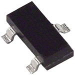
| 产品图片 |
|
| 产品型号 | ADM6328-28ARTZ-R7 |
| rohs | 无铅 / 符合限制有害物质指令(RoHS)规范要求 |
| 产品系列 | - |
| 供应商器件封装 | SOT-23-3 |
| 其它名称 | ADM6328-28ARTZ-R7CT |
| 包装 | 剪切带 (CT) |
| 受监控电压数 | 1 |
| 复位 | 低有效 |
| 复位超时 | 最小为 100 ms |
| 安装类型 | 表面贴装 |
| 封装/外壳 | TO-236-3,SC-59,SOT-23-3 |
| 工作温度 | -40°C ~ 85°C |
| 标准包装 | 1 |
| 电压-阈值 | 2.8V |
| 类型 | 简单复位/加电复位 |
| 输出 | 开路漏极或开路集电极 |
| 配用 | /product-detail/zh/EVAL-CN0276-SDPZ/EVAL-CN0276-SDPZ-ND/4571727 |


- 商务部:美国ITC正式对集成电路等产品启动337调查
- 曝三星4nm工艺存在良率问题 高通将骁龙8 Gen1或转产台积电
- 太阳诱电将投资9.5亿元在常州建新厂生产MLCC 预计2023年完工
- 英特尔发布欧洲新工厂建设计划 深化IDM 2.0 战略
- 台积电先进制程称霸业界 有大客户加持明年业绩稳了
- 达到5530亿美元!SIA预计今年全球半导体销售额将创下新高
- 英特尔拟将自动驾驶子公司Mobileye上市 估值或超500亿美元
- 三星加码芯片和SET,合并消费电子和移动部门,撤换高东真等 CEO
- 三星电子宣布重大人事变动 还合并消费电子和移动部门
- 海关总署:前11个月进口集成电路产品价值2.52万亿元 增长14.8%


PDF Datasheet 数据手册内容提取
Ultralow Power, 3-Lead, SOT-23 Microprocessor Reset Circuits Data Sheet ADM6326/ADM6328/ADM6346/ADM6348 FEATURES FUNCTIONAL BLOCK DIAGRAMS Ultralow supply current of 1 µA maximum (ADM6326/ADM6328) ADM6326/ADM6346 Accurate monitoring of 2.5 V, 3 V, 3.3 V, and 5 V rails Reset thresholds available in increments from 2.2 V to 4.63 V VCC RESET GENERATOR RESET Glitch immunity from negative-going VCC transients VREF (100ms) 2 reset output options Push-pull RESET (ADM6326/ADM6346) Open-drain RESET (ADM6328/ADM6348) GND 08052-001 Minimum reset timeout of 100 ms Figure 1. Operating temperature range of −40°C to +85°C 3-lead SOT-23 package ADM6328/ADM6348 APPLICATIONS VCC RESET RESET Telecommunications GENERATOR VREF (100ms) Microprocessor systems Desktop and notebook computers Portable equipment GND 08052-002 Figure 2. GENERAL DESCRIPTION The ADM6326/ADM6328/ADM6346/ADM6348 devices provide microprocessor in a reset state until conditions have stabilized. low cost solutions for protecting sensitive circuitry, such as micro- The reset output remains operational with VCC as low as 1 V. processor and telecommunications circuitry. The ADM6326 and ADM6346 have an active low push-pull reset With built-in glitch immunity, ultralow supply currents, and output. The ADM6328 and ADM6348 have an active low open- 24 reset threshold voltage options, the ADM6326/ADM6328/ drain reset output, which requires an external pull-up resistor. ADM6346/ADM6348 not only ensure that systems are immune The ADM6326 and ADM6328 offer a choice of ten reset thresholds to fast transients on V , but also that the devices are suitable in increments between 2.2 V and 3.08 V, whereas the ADM6346 CC for monitoring a variety of supply voltages in low power, and ADM6348 offer a choice of 14 reset thresholds between 3.3 V portable equipment. and 4.63 V. Not all options are released for sale as standard models. See the Ordering Guide for details. These devices provide a reset output during power-up, power- down, and brownout conditions. On power-up, an internal These devices are available in a 3-lead SOT-23 package and timer holds RESET asserted for at least 100 ms. This holds the operate over the extended temperature range of −40°C to +85°C. Rev. B Document Feedback Information furnished by Analog Devices is believed to be accurate and reliable. However, no responsibility is assumed by Analog Devices for its use, nor for any infringements of patents or other One Technology Way, P.O. Box 9106, Norwood, MA 02062-9106, U.S.A. rights of third parties that may result from its use. Specifications subject to change without notice. No license is granted by implication or otherwise under any patent or patent rights of Analog Devices. Tel: 781.329.4700 ©2009–2018 Analog Devices, Inc. All rights reserved. Trademarks and registered trademarks are the property of their respective owners. Technical Support www.analog.com
ADM6326/ADM6328/ADM6346/ADM6348 Data Sheet TABLE OF CONTENTS Features .............................................................................................. 1 Pin Configuration and Function Descriptions ..............................5 Applications ....................................................................................... 1 Typical Performance Characteristics ..............................................6 Functional Block Diagrams ............................................................. 1 Theory of Operation .........................................................................7 General Description ......................................................................... 1 Reset Output ..................................................................................7 Revision History ............................................................................... 2 Interfacing to Other Devices .......................................................7 Specifications ..................................................................................... 3 Transient Immunity ......................................................................7 Absolute Maximum Ratings ............................................................ 4 Outline Dimensions ..........................................................................8 Thermal Resistance ...................................................................... 4 Ordering Guide .............................................................................9 ESD Caution .................................................................................. 4 REVISION HISTORY 5/2018—Rev. A to Rev. B Changes to General Description Section ...................................... 1 Changes to Table 2 ............................................................................ 3 Added Note 1, Table 2; Renumbered Sequentially ....................... 3 Changes to Ordering Guide ............................................................ 9 6/2014—Rev. 0 to Rev. A Changes to Figure 1 and Figure 2 ................................................... 1 9/2009—Revision 0: Initial Version Rev. B | Page 2 of 9
Data Sheet ADM6326/ADM6328/ADM6346/ADM6348 SPECIFICATIONS T = −40°C to +85°C, unless otherwise noted. Typical values are at T = 25°C and V = 3 V. Overtemperature limits are guaranteed by design. A A CC Table 1. Parameter Min Typ Max Unit Test Conditions/Comments OPERATING VOLTAGE RANGE, VCC 1.0 5.5 V INPUT CURRENT, ICC 0.5 1.0 µA ADM6326/ADM6328 only, VCC = 3.0 V for VTH ≤ 2.93 V, VCC = 3.2 V for VTH > 2.93 V, no load 1.0 1.75 µA VCC = 5.5 V, no load RESET THRESHOLD Threshold Voltage, VTH (See Table 2) VTH − 2.5% VTH VTH + 2.5% V VTH − 1.5% VTH VTH + 1.5% V TA = 25°C Temperature Coefficient 40 ppm/°C Hysteresis ADM6326/ADM6328 6.3 mV ADM6346/ADM6348 9.5 mV TIMING CHARACTERISTICS VCC to Reset Delay (tRD) 20 µs VCC = VTH to (VTH − 100 mV) Reset Active Timeout Period (tRP) 100 185 280 ms RESET OUTPUT VOLTAGE LOW, VOL 0.3 V VCC > 2.1 V, ISINK = 1.6 mA, reset asserted 0.4 V VCC ≥ 1.2 V, ISINK = 100 μA, reset asserted RESET OUTPUT VOLTAGE HIGH, VOH 0.8 × VCC V ADM6326 only, VCC = 3.2 V, ISOURCE = 500 µA 0.8 × VCC V ADM6326/ADM6346 only, VCC = 4.5 V, ISOURCE = 800 µA, VTH ≤ 4.38 V 0.8 × VCC V ADM6326/ADM6346 only, VCC = VTH(MAX), ISOURCE = 800 µA, VTH ≥ 4.5 V OPEN-DRAIN RESET OUTPUT LEAKAGE CURRENT 0.1 µA Table 2. Reset Threshold Voltage TA = 25°C TA = −40°C to +85°C Parameter Min Typ Max Min Max Unit RESET THRESHOLD VOLTAGE (VTH)1 ADM6326-22, ADM6328-22 2.167 2.2 2.233 2.145 2.25 V ADM6328-23 2.285 2.32 2.355 2.262 2.375 V ADM6328-25 2.462 2.5 2.537 2.437 2.562 V ADM6326-26 2.591 2.63 2.669 2.564 2.696 V ADM6326-27, ADM6328-27 2.66 2.7 2.741 2.633 2.768 V ADM6328-28 2.758 2.8 2.842 2.73 2.87 V ADM6326-29 2.886 2.93 2.974 2.857 3.0 V ADM6326-30 2.955 3.00 3.045 2.925 3.075 V ADM6326-31 3.034 3.08 3.126 3.003 3.15 V ADM6348-33 3.25 3.3 3.35 3.217 3.383 V ADM6348-34 3.349 3.4 3.451 3.315 3.485 V ADM6348-35 3.447 3.5 3.552 3.412 3.587 V ADM6348-36 3.546 3.6 3.654 3.51 3.69 V ADM6348-37 3.644 3.7 3.755 3.607 3.792 V ADM6348-38 3.743 3.8 3.857 3.705 3.895 V ADM6348-39 3.841 3.9 3.958 3.802 3.997 V ADM6348-40 3.94 4.0 4.06 3.9 4.1 V ADM6348-41 4.038 4.1 4.161 3.997 4.202 V ADM6348-42 4.137 4.2 4.263 4.095 4.305 V ADM6348-43 4.235 4.3 4.364 4.192 4.407 V ADM6348-44 4.314 4.38 4.446 4.27 4.489 V ADM6348-45 4.432 4.5 4.567 4.387 4.612 V ADM6346-46, ADM6348-46 4.56 4.63 4.699 4.514 4.746 V 1 Not all device options are released for sale as standard models. See the Ordering Guide for full details. Rev. B | Page 3 of 9
ADM6326/ADM6328/ADM6346/ADM6348 Data Sheet ABSOLUTE MAXIMUM RATINGS THERMAL RESISTANCE Table 3. Parameter Rating θ is specified for the worst-case conditions, that is, a device JA Supply Voltage, V −0.3 V to +6 V soldered in a circuit board for surface-mount packages. CC Input Current, I 20 mA CC Table 4. Thermal Resistance Output Voltage Package Type θ Unit Push-Pull RESET −0.3 V to (VCC + 0.3 V) JA 3-Lead SOT-23 270 °C/W Open-Drain RESET −0.3 V to +6 V Output Current (RESET) 20 mA ESD CAUTION Rate of Rise of V 100 V/µs CC Temperature Storage −65°C to +155°C Operating −40°C to +85°C Soldering (10 sec) 300°C Stresses at or above those listed under Absolute Maximum Ratings may cause permanent damage to the product. This is a stress rating only; functional operation of the product at these or any other conditions above those indicated in the operational section of this specification is not implied. Operation beyond the maximum operating conditions for extended periods may affect product reliability. Rev. B | Page 4 of 9
Data Sheet ADM6326/ADM6328/ADM6346/ADM6348 PIN CONFIGURATION AND FUNCTION DESCRIPTIONS ADM6326/ GND 1 ADM6328/ ADM6346/ ADM6348 3 VCC RESET 2 (NToOt Pto V SIEcaWle) 08052-003 Figure 3. ADM6326/ADM6328/ADM6346/ADM6348 Pin Configuration Table 5. Pin Function Descriptions Pin No. Mnemonic Description 1 GND Ground Reference for All Signals; 0 V. 2 RESET Active Low Logic Output. This pin is low when VCC is less than the reset threshold; it remains low for 185 ms (typical) after V becomes greater than the reset threshold. CC 3 V Supply Voltage Being Monitored. CC Rev. B | Page 5 of 9
ADM6326/ADM6328/ADM6346/ADM6348 Data Sheet TYPICAL PERFORMANCE CHARACTERISTICS 1.0 280 0.9 260 A) 00..78 VCVCC C= =3. 35VV UT (ms) 240 NT (µ 0.6 MEO 220 CURRE 0.5 ESET TI 128000 UPPLY 00..34 VCC = 1.4V R-UP R 160 S E W 0.2 O 140 P 0.1 120 0–40 –20 0TEMPER20ATURE(°4C0) 60 80 08052-004 100–40 –20 0TEMPER2A0TURE (°4C0) 60 80 08052-007 Figure 4. Supply Current vs. Temperature Figure 6. Power-Up Reset Timeout vs. Temperature 800 250 s) 700 TION (µ 600 AY (µs) 200 A L R E DU 500 T D 150 NSIENT 400 N RESE A W 100 R 300 O T D MUM 200 WER- VOD = 10mV XI O 50 VOD = 20mV A P M 100 VOD = 200mV VOD = 100mV 0 0 1 RESET THRES10HOLD OVERDRIVE,1 V00TH – VCC (mV) 1000 08052-006 –40 –20 0TEMPER2A0TURE (°4C0) 60 80 08052-005 Figure 5. Maximum Transient Duration vs. Reset Threshold Overdrive Figure 7. Power-Down Reset Delay vs. Temperature Rev. B | Page 6 of 9
Data Sheet ADM6326/ADM6328/ADM6346/ADM6348 THEORY OF OPERATION The ADM6326/ADM6328/ADM6346/ADM6348 are designed INTERFACING TO OTHER DEVICES to protect the integrity of a system’s operation by ensuring the The active low, open-drain reset output of the ADM6328 and proper operation of the system during power-up, power-down, ADM6348 makes these devices ideal for integration with devices and brownout conditions. Ultralow supply currents make these such as microprocessors with bidirectional reset pins. Simply devices particularly suitable for use in low power, portable connect the RESET output of the ADM6328 or ADM6348 to equipment. the RESET input of the microprocessor using a single pull-up RESET OUTPUT resistor to allow either device to initiate a system reset (see The ADM6326 and ADM6346 have an active low, push-pull Figure 8). reset output, whereas the ADM6328 and ADM6348 have an VCC active low, open-drain reset output, which requires an external pull-up resistor. The RESET signal is guaranteed to be valid for VCC RPULL-UP VCC V down to 1 V. MICROPROCESSOR CC ADM6328/ADM6348 SYSTEM When the ADM6326/ADM6328/ADM6346/ADM6348 are RESET powered up, the RESET output remains low for a period typically RESET INPUT GND GND eaqlluoawl st oa dtheeq uRaEtSeE tTim aec tfiover ttihme esoyustte pmer tiood p oofw 1e8r5 u mp sc. oTrhriesc ftelyat aunred 08052-008 Figure 8. Interfacing to a Microprocessor with a Bidirectional Reset Pin for the power supply to stabilize before any devices are brought out of reset and are allowed to begin executing instructions. Initializing TRANSIENT IMMUNITY a system in this way provides a more reliable startup for micro- To avoid unnecessary resets caused by fast power supply transients, processor systems. the ADM6326/ADM6328/ADM6346/ADM6348 provide glitch When the monitored voltage falls below its associated threshold immunity from negative-going V transients. CC (V ), RESET is asserted within 20 μs (typical). Asserting RESET TH Figure 5 shows the RESET comparator overdrive (that is, the this quickly means that the entire system can be reset at once maximum magnitude of negative-going pulses with respect to before any part of the system’s voltage falls below its recommended the typical threshold) vs. the pulse duration without a reset. operating voltage. This system reset can avoid dangerous and/or erroneous operation of a microprocessor based system. VCC VTH VTH VCC 1V 0V VCC RESET 0V tRP tRD 08052-009 Figure 9. RESET Timing Rev. B | Page 7 of 9
ADM6326/ADM6328/ADM6346/ADM6348 Data Sheet OUTLINE DIMENSIONS 3.04 2.90 2.80 1.40 1.30 1.20 3 2.64 2.10 1 2 0.60 1.03 0.45 0.89 2.05 1.02 1.78 0.95 0.54 REF 0.88 1.12 GAUGE 0.89 PLANE 0.100 0.180 0.013 0.085 0.51 SEPALTAINNGE 0.37 0.25 0.60 MAX 0.30 MIN COMPLIANTTO JEDEC STANDARDSTO-236-AB 011909-C Figure 10. 3-Lead Small Outline Transistor Package [SOT-23-3] (RT-3) Dimensions shown in millimeters Rev. B | Page 8 of 9
Data Sheet ADM6326/ADM6328/ADM6346/ADM6348 ORDERING GUIDE Typical Threshold RESET Output Marking Model1, 2 Voltage (T = 25°C) Structure Package Description Package Option Code A ADM6326-22ARTZ-R7 2.2 V Push-Pull 3-Lead SOT-23 RT-3 LAQ ADM6326-26ARTZ-R7 2.63 V Push-Pull 3-Lead SOT-23 RT-3 LAU ADM6326-27ARTZ-R7 2.7 V Push-Pull 3-Lead SOT-23 RT-3 LAV ADM6326-29ARTZ-R7 2.93 V Push-Pull 3-Lead SOT-23 RT-3 LAX ADM6326-30ARTZ-R7 3.0 V Push-Pull 3-Lead SOT-23 RT-3 LAY ADM6326-31ARTZ-R7 3.08 V Push-Pull 3-Lead SOT-23 RT-3 LAZ ADM6328-22ARTZ-R7 2.2 V Open-Drain 3-Lead SOT-23 RT-3 LB0 ADM6328-23ARTZ-R7 2.32 V Open-Drain 3-Lead SOT-23 RT-3 LB1 ADM6328-25ARTZ-R7 2.5 V Open-Drain 3-Lead SOT-23 RT-3 LB3 ADM6328-27ARTZ-R7 2.7 V Open-Drain 3-Lead SOT-23 RT-3 LB5 ADM6328-28ARTZ-R7 2.8 V Open-Drain 3-Lead SOT-23 RT-3 LB6 ADM6346-46ARTZ-R7 4.63 V Push-Pull 3-Lead SOT-23 RT-3 LCU ADM6348-33ARTZ-R7 3.3 V Open-Drain 3-Lead SOT-23 RT-3 LCV ADM6348-34ARTZ-R7 3.4 V Open-Drain 3-Lead SOT-23 RT-3 LCW ADM6348-35ARTZ-R7 3.5 V Open-Drain 3-Lead SOT-23 RT-3 LCX ADM6348-36ARTZ-R7 3.6 V Open-Drain 3-Lead SOT-23 RT-3 LCY ADM6348-37ARTZ-R7 3.7 V Open-Drain 3-Lead SOT-23 RT-3 LCZ ADM6348-38ARTZ-R7 3.8 V Open-Drain 3-Lead SOT-23 RT-3 LD0 ADM6348-39ARTZ-R7 3.9 V Open-Drain 3-Lead SOT-23 RT-3 LD1 ADM6348-40ARTZ-R7 4.0 V Open-Drain 3-Lead SOT-23 RT-3 LD2 ADM6348-41ARTZ-R7 4.1 V Open-Drain 3-Lead SOT-23 RT-3 LD3 ADM6348-42ARTZ-R7 4.2 V Open-Drain 3-Lead SOT-23 RT-3 LD4 ADM6348-43ARTZ-R7 4.3 V Open-Drain 3-Lead SOT-23 RT-3 LD5 ADM6348-44ARTZ-R7 4.38 V Open-Drain 3-Lead SOT-23 RT-3 LD6 ADM6348-45ARTZ-R7 4.5 V Open-Drain 3-Lead SOT-23 RT-3 LD7 ADM6348-46ARTZ-R7 4.63 V Open-Drain 3-Lead SOT-23 RT-3 LD8 1 The ADM6326/ADM6328/ADM6346/ADM6348 include many device options; however, not all options are released for sale. Released options are called standard models and are listed in the Ordering Guide. For the most up to date list of standard models, check the Single Supply Monitors IC page on the Analog Devices website. Contact sales for information on nonstandard models and be aware that samples and production units have very long lead times. 2 Z = RoHS Compliant Part. ©2009–2018 Analog Devices, Inc. All rights reserved. Trademarks and registered trademarks are the property of their respective owners. D08052-0-5/18(B) Rev. B | Page 9 of 9