ICGOO在线商城 > 集成电路(IC) > 接口 - 驱动器,接收器,收发器 > ADM485ARMZ-REEL7

 Datasheet下载
- 型号: ADM485ARMZ-REEL7
- 制造商: Analog
- 库位|库存: xxxx|xxxx
- 要求:
| 数量阶梯 | 香港交货 | 国内含税 |
| +xxxx | $xxxx | ¥xxxx |
查看当月历史价格
查看今年历史价格
ADM485ARMZ-REEL7产品简介:
ICGOO电子元器件商城为您提供ADM485ARMZ-REEL7由Analog设计生产,在icgoo商城现货销售,并且可以通过原厂、代理商等渠道进行代购。 ADM485ARMZ-REEL7价格参考。AnalogADM485ARMZ-REEL7封装/规格:接口 - 驱动器,接收器,收发器, 半 收发器 1/1 RS422,RS485 8-MSOP。您可以下载ADM485ARMZ-REEL7参考资料、Datasheet数据手册功能说明书,资料中有ADM485ARMZ-REEL7 详细功能的应用电路图电压和使用方法及教程。
ADM485ARMZ-REEL7 是由 Analog Devices Inc. 生产的一款接口芯片,属于驱动器、接收器和收发器类别。它主要用于 RS-485 和 RS-422 通信标准的实现,适用于需要高可靠性和长距离数据传输的应用场景。

 应用场景:

1. 工业自动化:
   - 在工业控制系统中,ADM485ARMZ-REEL7 可用于连接PLC(可编程逻辑控制器)、传感器、执行器等设备。RS-485 标准支持多点通信,允许多个设备通过同一总线进行通信,适合工厂自动化、楼宇自动化等场景。

2. 楼宇自动化:
   - 该芯片可用于智能建筑中的照明控制、温度监控、安防系统等。通过 RS-485 总线,可以实现不同楼层或区域之间的设备互联,确保数据的稳定传输。

3. 远程监控与数据采集 (SCADA):
   - 在电力、石油、天然气等行业中,ADM485ARMZ-REEL7 可用于远程监控和数据采集系统。它能够将分布在广阔区域的传感器数据传输到中央控制系统,确保实时监控和故障诊断。

4. 交通与运输:
   - 在轨道交通、高速公路监控等领域,该芯片可用于车辆与地面系统的通信,如列车状态监控、信号传输等。其抗干扰能力强,适合复杂电磁环境下的应用。

5. 医疗设备:
   - 在医疗设备中,ADM485ARMZ-REEL7 可用于连接不同的仪器和监测设备,确保数据的准确传输。例如,医院的监护系统可以通过 RS-485 总线将多个病床的数据集中管理。

6. 安防监控:
   - 在视频监控系统中,ADM485ARMZ-REEL7 可用于摄像机、门禁系统等设备之间的通信,确保图像和控制指令的可靠传输。

 特性优势:
- 高抗噪能力:该芯片具有出色的共模噪声抑制能力,能够在嘈杂的工业环境中保持稳定的通信。
- 低功耗设计:适用于对功耗敏感的应用,如电池供电的设备。
- 宽工作电压范围:支持 3V 至 5.5V 的电源电压,适应多种应用场景。
- ESD 保护:内置静电放电保护功能,提高芯片的可靠性。

综上所述,ADM485ARMZ-REEL7 适用于各种需要可靠、高效、长距离数据传输的工业和商业应用,特别是在多点通信和复杂电磁环境下表现出色。
| 参数 | 数值 |
| 产品目录 | 集成电路 (IC)半导体 |
| 描述 | IC TXRX RS-485 5V 5MBPS 8MSOPRS-422/RS-485 接口 IC 5V Low Pwr 5Mbps Half Duplex |
| Duplex | Half Duplex |
| 产品分类 | |
| 品牌 | Analog Devices Inc |
| 产品手册 | |
| 产品图片 |
|
| rohs | 符合RoHS无铅 / 符合限制有害物质指令(RoHS)规范要求 |
| 产品系列 | 接口 IC,RS-422/RS-485 接口 IC,Analog Devices ADM485ARMZ-REEL7- |
| 数据手册 | |
| 产品型号 | ADM485ARMZ-REEL7 |
| PCN组件/产地 | |
| 产品种类 | RS-422/RS-485 接口 IC |
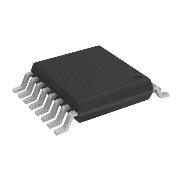
| 供应商器件封装 | 8-MSOP |
| 关闭 | No |
| 其它名称 | ADM485ARMZ-REEL7DKR |
| 功能 | Transceiver |
| 包装 | Digi-Reel® |
| 协议 | RS422,RS485 |
| 双工 | 半 |
| 商标 | Analog Devices |
| 安装类型 | 表面贴装 |
| 安装风格 | SMD/SMT |
| 封装 | Reel |
| 封装/外壳 | 8-TSSOP,8-MSOP(0.118",3.00mm 宽) |
| 封装/箱体 | MSOP-8 |
| 工作温度 | -40°C ~ 85°C |
| 工作温度范围 | - 40 C to + 85 C |
| 工作电源电压 | 5 V |
| 工厂包装数量 | 1000 |
| 接收器滞后 | 70mV |
| 接收机数量 | 1 Receiver |
| 数据速率 | 5Mbps |
| 最大工作温度 | + 85 C |
| 最小工作温度 | - 40 C |
| 标准包装 | 1 |
| 激励器数量 | 1 Driver |
| 电压-电源 | 4.75 V ~ 5.25 V |
| 电源电流 | 2.2 mA |
| 类型 | 收发器 |
| 系列 | ADM485 |
| 输出类型 | 3-State |
| 驱动器/接收器数 | 1/1 |


- 商务部:美国ITC正式对集成电路等产品启动337调查
- 曝三星4nm工艺存在良率问题 高通将骁龙8 Gen1或转产台积电
- 太阳诱电将投资9.5亿元在常州建新厂生产MLCC 预计2023年完工
- 英特尔发布欧洲新工厂建设计划 深化IDM 2.0 战略
- 台积电先进制程称霸业界 有大客户加持明年业绩稳了
- 达到5530亿美元!SIA预计今年全球半导体销售额将创下新高
- 英特尔拟将自动驾驶子公司Mobileye上市 估值或超500亿美元
- 三星加码芯片和SET,合并消费电子和移动部门,撤换高东真等 CEO
- 三星电子宣布重大人事变动 还合并消费电子和移动部门
- 海关总署:前11个月进口集成电路产品价值2.52万亿元 增长14.8%


PDF Datasheet 数据手册内容提取
5 V Low Power EIA RS-485 Transceiver ADM485 FEATURES FUNCTIONAL BLOCK DIAGRAM Meets EIA RS-485 standard ADM485 5 Mbps data rate Single 5 V supply RO 1 R 8 VCC –7 V to +12 V bus common-mode range High speed, low power BiCMOS RE 2 7 B Thermal shutdown protection DE 3 6 A Short-circuit protection Driver propagation delay: 10 ns typical DI 4 D 5 GND RHeigchei-vZe or uptrpouptasg waittiho np odweleary o: 1ff5 ns typical 00078-001 Superior upgrade for LTC485 Figure 1. APPLICATIONS Low power RS-485 systems DTE/DCE interface Packet switching Local area networks (LNAs) Data concentration Data multiplexers Integrated services digital network (ISDN) GENERAL DESCRIPTION The ADM485 is a differential line transceiver suitable for high The receiver contains a fail-safe feature that results in a logic speed bidirectional data communication on multipoint bus high output state if the inputs are unconnected (floating). transmission lines. It is designed for balanced data transmission The ADM485 is fabricated on BiCMOS, an advanced mixed and complies with EIA standards RS-485 and RS-422. The part technology process combining low power CMOS with fast contains a differential line driver and a differential line receiver. switching bipolar technology. All inputs and outputs contain Both the driver and the receiver can be enabled independently. protection against ESD; all driver outputs feature high source When disabled, the outputs are three-stated. and sink current capability. An epitaxial layer is used to guard The ADM485 operates from a single 5 V power supply. against latch-up. Excessive power dissipation caused by bus contention or by The ADM485 features extremely fast switching speeds. Minimal output shorting is prevented by a thermal shutdown circuit. If driver propagation delays permit transmission at data rates up during fault conditions, a significant temperature increase is to 5 Mbps while low skew minimizes EMI interference. detected in the internal driver circuitry, this feature forces the The part is fully specified over the commercial and industrial driver output into a high impedance state. temperature range and is available in 8-lead PDIP, 8-lead SOIC, Up to 32 transceivers can be connected simultaneously on a and small footprint, 8-lead MSOP packages. bus, but only one driver should be enabled at any time. It is important, therefore, that the remaining disabled drivers do not load the bus. To ensure this, the ADM485 driver features high output impedance when disabled and when powered down, which minimizes the loading effect when the transceiver is not being used. The high impedance driver output is maintained over the common-mode voltage range of −7 V to +12 V. Rev. F Information furnished by Analog Devices is believed to be accurate and reliable. However, no responsibility is assumed by Analog Devices for its use, nor for any infringements of patents or other One Technology Way, P.O. Box 9106, Norwood, MA 02062-9106, U.S.A. rights of third parties that may result from its use. Specifications subject to change without notice. No license is granted by implication or otherwise under any patent or patent rights of Analog Devices. Tel: 781.329.4700 www.analog.com Trademarks and registered trademarks are the property of their respective owners. Fax: 781.461.3113 ©1993–2008 Analog Devices, Inc. All rights reserved.
ADM485 TABLE OF CONTENTS Features..............................................................................................1 Test Circuits.....................................................................................10 Applications.......................................................................................1 Switching Characteristics..............................................................11 Functional Block Diagram..............................................................1 Applications Information..............................................................12 General Description.........................................................................1 Differential Data Transmission................................................12 Revision History...............................................................................2 Cable and Data Rate...................................................................12 Specifications.....................................................................................3 Thermal Shutdown....................................................................12 Timing Specifications..................................................................4 Propagation Delay......................................................................12 Absolute Maximum Ratings............................................................5 Receiver Open Circuit, Fail-Safe..............................................12 ESD Caution..................................................................................5 Outline Dimensions.......................................................................13 Pin Configuration and Function Descriptions.............................6 Ordering Guide..........................................................................14 Typical Performance Characteristics.............................................7 REVISION HISTORY 04/08—Rev. E to Rev. F 1/03—Rev. B to Rev. C. Updated Format..................................................................Universal Change to Specifications..................................................................2 Changes to Table 2............................................................................4 Change to Ordering Guide...............................................................3 Updated Outline Dimension.........................................................13 12/02—Rev. A to Rev. B. Changes to Ordering Guide..........................................................14 Deleted Q-8 Package..........................................................Universal 10/03—Rev. D to Rev. E Edits to Features.................................................................................1 Changes to Timing Specifications..................................................2 Edits to General Description...........................................................1 Updated Ordering Guide.................................................................3 Edits, additions to Specifications.....................................................2 Edits, additions to Absolute Maximum Ratings............................3 7/03—Rev. C to Rev. D Additions to Ordering Guide...........................................................3 Changes to Absolute Maximum Ratings.......................................3 TPCs Updated and Reformatted.....................................................5 Changes to Ordering Guide............................................................3 Addition of 8-Lead MSOP Package................................................9 Update to Outline Dimensions.......................................................9 Update to Outline Dimensions........................................................9 Rev. F | Page 2 of 16
ADM485 SPECIFICATIONS V = 5 V ± 5%, all specifications T to T , unless otherwise noted. CC MIN MAX Table 1. Parameter Min Typ Max Unit Test Conditions/Comments DRIVER Differential Output Voltage, V 5.0 V R = ∞, see Figure 20 OD 2.0 5.0 V V = 5 V, R = 50 Ω (RS-422), see Figure 20 CC 1.5 5.0 V R = 27 Ω (RS-485), see Figure 20 V 1.5 5.0 V V = −7 V to +12 V, see Figure 21 OD3 TST Δ|V | for Complementary Output States 0.2 V R = 27 Ω or 50 Ω, see Figure 20 OD Common-Mode Output Voltage, V 3 V R = 27 Ω or 50 Ω, see Figure 20 OC Δ|V | for Complementary Output States 0.2 V R = 27 Ω or 50 Ω OD Output Short-Circuit Current, V = High 35 250 mA −7 V ≤ V ≤ +12 V OUT O Output Short-Circuit Current, V = Low 35 250 mA −7 V ≤ V ≤ +12 V OUT O CMOS Input Logic Threshold Low, V 0.8 V INL CMOS Input Logic Threshold High, V 2.0 V INH Logic Input Current (DE, DI) ±1.0 μA RECEIVER Differential Input Threshold Voltage, V −0.2 +0.2 V −7 V ≤ V ≤ +12 V TH CM Input Voltage Hysteresis, ΔV 70 mV V = 0 V TH CM Input Resistance 12 kΩ −7 V ≤ V ≤ +12 V CM Input Current (A, B) 1 mA V = 12 V IN –0.8 mA V = −7 V IN CMOS Input Logic Threshold Low, V 0.8 V INL CMOS Input Logic Threshold High, V 2.0 V INH Logic Enable Input Current (RE) ±1 μA CMOS Output Voltage Low, V 0.4 V I = 4.0 mA OL OUT CMOS Output Voltage High, V 4.0 V I = −4.0 mA OH OUT Short-Circuit Output Current 7 85 mA V = GND or V OUT CC Three-State Output Leakage Current ±1.0 μA 0.4 V ≤ V ≤ 2.4 V OUT POWER SUPPLY CURRENT ICC, Outputs Enabled 1.0 2.2 mA Digital inputs = GND or VCC ICC, Outputs Disabled 0.6 1 mA Digital inputs = GND or VCC Rev. F | Page 3 of 16
ADM485 TIMING SPECIFICATIONS V = 5 V ± 5%, all specifications T to T , unless otherwise noted. CC MIN MAX Table 2. Parameter Min Typ Max Unit Test Conditions/Comments DRIVER Propagation Delay Input to Output, t , t 2 10 15 ns R = 54 Ω, C = C = 100 pF, see Figure 22 PLH PHL LDIFF L1 L2 Driver Output to OUTPUT, tSKEW 1 5 ns RLDIFF = 54 Ω, CL1 = CL2 = 100 pF, see Figure 22 Driver Rise/Fall Time, t, t 8 15 ns R = 54 Ω, C = C = 100 pF, see Figure 22 R F LDIFF L1 L2 Driver Enable to Output Valid 10 25 ns R = 110 Ω, C = 50 pF, see Figure 23 L L Driver Disable Timing 10 25 ns R = 110 Ω, C = 50 pF, see Figure 23 L L Matched Enable Switching |t − t | 0 2 ns R = 110 Ω, C = 50 pF, see Figure 231 ZH ZL L L Matched Disable Switching |t − t | 0 2 ns R = 110 Ω, C = 50 pF, see Figure 231 HZ LZ L L RECEIVER Propagation Delay Input to Output, t , t 8 15 30 ns C = 15 pF, see Figure 24 PLH PHL L Skew |t − t | 5 ns C = 15 pF, see Figure 24 PLH PHL L Receiver Enable, t , t 5 20 ns C = 15 pF, R = 1 kΩ, see Figure 25 ZH ZL L L Receiver Disable, t , t 5 20 ns C = 15 pF, R = 1 kΩ, see Figure 25 HZ LZ L L Tx Pulse Width Distortion 1 ns Rx Pulse Width Distortion 1 ns 1 Guaranteed by characterization. Rev. F | Page 4 of 16
ADM485 ABSOLUTE MAXIMUM RATINGS T = 25°C, unless otherwise noted. Table 4. Transmitting A Inputs Outputs Table 3. DE DI B A Parameter Rating 1 1 0 1 V −0.3 V to +7 V CC 1 0 1 0 Inputs 0 X1 Z2 Z2 Driver Input (DI) −0.3 V to V + 0.3 V CC Control Inputs (DE, RE) −0.3 V to V + 0.3 V 1 X = don’t care. CC 2 Z = high impedance. Receiver Inputs (A, B) −9 V to +14 V Outputs Table 5. Receiving Driver Outputs (A, B) −9 V to +14 V RE Input A − Input B Output RO Receiver Output −0.5 V to V + 0.5 V CC 0 ≥ +0.2 V 1 Power Dissipation 8-Lead MSOP 900 mW 0 ≤ −0.2 V 0 θ , Thermal Impedance 206°C/W JA 0 Inputs open 1 Power Dissipation 8-Lead PDIP 500 mW 1 X1 Z2 θ , Thermal Impedance 130°C/W JA Power Dissipation 8-Lead SOIC 450 mW 1 X = don’t care. 2 Z = high impedance. θ , Thermal Impedance 170°C/W JA Operating Temperature Range Commercial Range (J Version) 0°C to 70°C ESD CAUTION Industrial Range (A Version) −40°C to +85°C Storage Temperature Range −65°C to +150°C Lead Temperature (Soldering, 10 sec) 300°C Vapor Phase (60 sec) 215°C Infrared (15 sec) 220°C Stresses above those listed under Absolute Maximum Ratings may cause permanent damage to the device. This is a stress rating only; functional operation of the device at these or any other conditions above those indicated in the operational section of this specification is not implied. Exposure to absolute maximum rating conditions for extended periods may affect device reliability. Rev. F | Page 5 of 16
ADM485 PIN CONFIGURATION AND FUNCTION DESCRIPTIONS RO 1 8 VCC RE 2 ADM485 7 B TOP VIEW DDEI 34 (Not to Scale) 65 AGND00078-002 Figure 2. Pin Configuration Table 6. Pin Function Descriptions Pin No. Mnemonic Function 1 RO Receiver Output. When enabled, if A is greater than B by 200 mV, RO is high. If A is less than B by 200 mV, RO is low. 2 RE Receiver Output Enable. A low level enables the receiver output, RO. A high level places it in a high impedance state. 3 DE Driver Output Enable. A high level enables the driver differential outputs, A and B. A low level places it in a high impedance state. 4 DI Driver Input. When the driver is enabled, a logic low on DI forces A low and B high, while a logic high on DI forces A high and B low. 5 GND Ground Connection, 0 V. 6 A Noninverting Receiver Input A/Driver Output A. 7 B Inverting Receiver Input B/Driver Output B. 8 V Power Supply, 5 V ± 5%. CC Rev. F | Page 6 of 16
ADM485 TYPICAL PERFORMANCE CHARACTERISTICS 50 0.40 I = 8mA 45 V) 40 E ( 0.35 G mA)35 LTA NT (30 W VO 0.30 RE O UR25 T L C U UTPUT 2105 R OUTP 0.25 O E V 10 EI 0.20 C E 5 R 00 0.25 RE0C.5E0IVER0 .O75UTPU1T.0 0LOW 1V.2O5LTAG1.E50 (V) 1.75 2.00 00078-003 0.15–50 –25 0 TEMP25ERATUR5E0 (°C) 75 100 12500078-006 Figure 3. Output Current vs. Receiver Output Low Voltage Figure 6. Receiver Output Low Voltage vs. Temperature 0 90 –2 80 –4 70 A) A) m –6 m 60 T ( T ( N N RE –8 RE 50 R R U U C–10 C 40 T T U U TP–12 TP 30 U U O O –14 20 –16 10 –183.50 3.75RECEIV4E.0R0 OUTPU4T.2 H5IGH VO4L.5T0AGE (V4).75 5.00 00078-004 00 0.5DRIV1E.0R DIF1F.5EREN2T.0IAL O2U.5TPUT3 .V0OLTA3.G5E (V4).0 4.5 00078-007 Figure 4. Output Current vs. Receiver Output High Voltage Figure 7. Output Current vs. Driver Differential Output Voltage 4.55 2.15 I = 8mA V) GE (V) 4.50 TAGE ( 2.10 RL = 26.8Ω OLTA 4.45 T VOL GH V 4.40 UTPU 2.05 HI O T 4.35 L U A OUTP 4.30 RENTI 2.00 R E CEIVE 4.25 R DIFF 1.95 RE 4.20 VE RI D 4.1–550 –25 0 TEM2P5ERATUR5E0 (°C) 75 100 12500078-005 1.9–050 –25 0 TEM2P5ERATUR50E (°C) 75 100 12500078-008 Figure 5. Receiver Output High Voltage vs. Temperature Figure 8. Driver Differential Output Voltage vs. Temperature Rev. F | Page 7 of 16
ADM485 0.7 100 90 0.6 80 URRENT (mA) 657000 R SKEW (ns) 00..45 |tPLH–tPHL | UT C 40 EIVE 0.3 P C T E U 30 R 0.2 O 20 0.1 10 00 0.5 1D.0RIVE1R. 5OUTP2U.0T LO2W.5 VOL3T.A0GE (3V.5) 4.0 4.500078-009 –050 –25 0 TEMP25ERATUR50E (°C) 75 100 12500078-012 Figure 9. Output Current vs. Driver Output Low Voltage Figure 12. Receiver Skew vs. Temperature 0 6 –10 –20 5 A –30 m – –40 s) 4 ENT –50 W (n R E UR –60 SK 3 C R UT –70 VE |tPHLA–tPHLB | UTP –80 DRI 2 O –90 –100 1 |tPLHA–tPLHB | –110 –1200 0.5 1.0DRIV1E.5R OU2T.0PUT2 H.5IGH 3V.O0LTA3.G5E (V4).0 4.5 5.000078-010 0–50 –25 0 TEM2P5ERATUR5E0 (°C) 75 100 125 00078-013 Figure 10. Output Current vs. Driver Output High Voltage Figure 13. Driver Skew vs. Temperature 1.1 1.4 1.0 1.2 DRIVER ENABLED A) 1.0 m0.9 T ( N E 0.8 URR0.8 WD |tPLH–tPHL | C P Y 0.6 L PP0.7 SU DRIVER DISABLED 0.4 0.6 0.2 0.–550 –25 0 TEMP25ERATUR5E0 (°C) 75 100 12500078-011 –050 –25 0 T2E5MPERA50TURE (7°5C) 100 125 150 00078-014 Figure 11. Supply Current vs. Temperature Figure 14. Driver Pulse Width Distortion (PWD) vs. Temperature Rev. F | Page 8 of 16
ADM485 T 4 DI T A A B B 1,2 1,2 3 RO CH1 1.00VΩBW CH2 1.00VΩBW M5.00ns CH3 2.64V 00078-015 CCHH31 51..0000VVΩΩBBWW CCHH24 12..0000VVΩΩBBWW M10.00ns CH4 2.76V 00078-018 Figure 15. Unloaded Driver Differential Outputs Figure 18. Driver/Receiver Propagation Delays, High to Low A A B B 1,2 CH1 1.00VΩBW CH2 500mVΩBW M5.00ns CH3 2.74V 00078-016 1,2 CH1 500mVΩ CH2 500mVΩ M10.00ns CH4 2.76V 00078-019 Figure 16. Loaded Driver Differential Outputs Figure 19. Driver Output at 30 Mbps DI T 4 A B 1,2 RO 3 CCHH31 51..0000VVΩΩBBWW CCHH24 12..0000VVΩΩBBWW M10.0ns CH4 400mV 00078-017 Figure 17. Driver/Receiver Propagation Delays, Low to High Rev. F | Page 9 of 16
ADM485 TEST CIRCUITS R VCC A VOD RL 0V OR 3V S1 S2 DE R VOC 00078-020 DE IN B CL VOUT 00078-023 Figure 20. Driver Voltage Measurement Figure 23. Driver Enable/Disable 375Ω A VOD3 60Ω VTST RE VOUT B 375Ω 00078-021 CL 00078-024 Figure 21. Driver Voltage Measurement Figure 24. Receiver Propagation Delay +1.5V VCC A CL1 S1 RL RLDIFF –1.5V RE S2 B CL2 00078-022 REIN CL VOUT 00078-025 Figure 22. Driver Propagation Delay Figure 25. Receiver Enable/Disable Rev. F | Page 10 of 16
ADM485 SWITCHING CHARACTERISTICS 3V 1.5V 1.5V 0V t PLH t PHL A, B 0V 0V B 1/2VO VO A tPLH tPHL tSKEW=tPLH–tPHL VOH +VO 90% POINT 90% POINT RO –V0VO 10% POINT tR tF 10% POINT 00078-026 1.5V tSKEW=tPLH–tPHL 1.5V VOL00078-028 Figure 26. Driver Propagation Delay, Rise/Fall Timing Figure 28. Receiver Propagation Delay 3V 3V 1.5V 1.5V RE DE 1.5V 1.5V 0V t t 0V tZL tLZ ZL LZ 1.5V A, B 2.3V VOL + 0.5V RO OUTPUT LOW VOL + 0.5V VOL VOL t t ZH HZ t t ZH HZ OUTPUT HIGH VOH VOH A, B 2.3V VOH – 0.5V 0V 00078-027 R0OV 1.5V VOH – 0.5V 00078-029 Figure 27. Driver Enable/Disable Timing Figure 29. Receiver Enable/Disable Timing Rev. F | Page 11 of 16
ADM485 APPLICATIONS INFORMATION DIFFERENTIAL DATA TRANSMISSION Differential data transmission is used to reliably transmit data at RT RT high rates over long distances and through noisy environments. Differential transmission nullifies the effects of ground shifts D D and noise signals that appear as common-mode voltages on the line. There are two main standards approved by the EIA that specify the electrical characteristics of transceivers used in R R differential data transmission. The RS-422 standard specifies data rates up to 10 MBaud and line lengths up to 4000 ft. A single driver can drive a transmission R R line with up to 10 receivers. D D To cater to true multipoint communications, the RS-485 00078-030 standard was defined. This standard meets or exceeds all the Figure 30. Typical RS-485 Network requirements of RS-422 but also allows for up to 32 drivers and As with any transmission line, it is important that reflections be 32 receivers to be connected to a single bus. An extended common- minimized. This can be achieved by terminating the extreme ends mode range of −7 V to +12 V is defined. The most significant of the line using resistors equal to the characteristic impedance of difference between the RS-422 standard and the RS-485 standard is the line. Stub lengths of the main line should also be kept as the fact that the drivers can be disabled, thereby allowing more short as possible. A properly terminated transmission line appears than one (32 in fact) to be connected to a single line. Only one purely resistive to the driver. driver should be enabled at a time, but the RS-485 standard THERMAL SHUTDOWN contains additional specifications to guarantee device safety in the event of line contention. The ADM485 contains thermal shutdown circuitry that protects the part from excessive power dissipation during fault conditions. Table 7. Comparison of RS-422 and RS-485 Interface Standards Shorting the driver outputs to a low impedance source can result Specification RS-422 RS-485 in high driver currents. The thermal sensing circuitry detects Transmission Type Differential Differential the increase in die temperature and disables the driver outputs. Maximum Cable Length 4000 ft. 4000 ft. The thermal sensing circuitry is designed to disable the driver Minimum Driver Output Voltage ±2 V ±1.5 V outputs when a die temperature of 150°C is reached. As the Driver Load Impedance 100 Ω 54 Ω device cools, the drivers are re-enabled at 140°C. Receiver Input Resistance 4 kΩ min 12 kΩ min PROPAGATION DELAY Receiver Input Sensitivity ±200 mV ±200 mV Receiver Input Voltage Range −7 V to +7 V −7 V to +12 V The ADM485 features very low propagation delay, ensuring No. of Drivers/Receivers per Line 1/10 32/32 maximum baud rate operation. The driver is well balanced, ensuring distortion free transmission. CABLE AND DATA RATE Another important specification is a measure of the skew The transmission line of choice for RS-485 communications is between the complementary outputs. Excessive skew impairs a twisted pair. Twisted pair cable tends to cancel common-mode the noise immunity of the system and increases the amount of noise and causes cancellation of the magnetic fields generated electromagnetic interference (EMI). by the current flowing through each wire, thereby reducing the RECEIVER OPEN CIRCUIT, FAIL-SAFE effective inductance of the pair. The receiver input includes a fail-safe feature that guarantees a The ADM485 is designed for bidirectional data communications logic high on the receiver when the inputs are open circuit or on multipoint transmission lines. A typical application showing floating. a multipoint transmission network is illustrated in Figure 30. An RS-485 transmission line can have as many as 32 transceivers on the bus. Only one driver can transmit at a particular time, but multiple receivers can be enabled simultaneously. Rev. F | Page 12 of 16
ADM485 OUTLINE DIMENSIONS 5.00(0.1968) 4.80(0.1890) 8 5 4.00 (0.1574) 6.20 (0.2441) 3.80 (0.1497) 1 4 5.80 (0.2284) 1.27 (0.0500) 0.50 (0.0196) BSC 1.75 (0.0688) 0.25 (0.0099) 45° 0.25 (0.0098) 1.35 (0.0532) 8° 0.10 (0.0040) 0° COPLANARITY 0.51 (0.0201) 0.10 SEATING 0.31 (0.0122) 0.25 (0.0098) 10..2470 ((00..00510507)) PLANE 0.17 (0.0067) COMPLIANTTO JEDEC STANDARDS MS-012-AA C(RINOEFNPETARRREOENNLCLTEIHN EOGSN DELSIYM)AEANNRDSEI AORRNOESU NANORDEET DAIN-PO MPFRIFLO LMPIIMRLELIATIMTEEER TFSEO; RIRN ECUQHSU EDI VIINMA LEDENENSSTIIOGSN NFS.OR 012407-A Figure 31. 8-Lead Standard Small Outline Package [SOIC_N] Narrow Body (R-8) Dimensions shown in millimeters and (inches) 3.20 3.00 2.80 8 5 5.15 3.20 4.90 3.00 4.65 2.80 1 4 PIN 1 0.65 BSC 0.95 0.85 1.10 MAX 0.75 0.80 0.15 0.38 0.23 8° 0.60 0.00 0.22 0.08 0° 0.40 COPLANARITY SEATING 0.10 PLANE COMPLIANT TO JEDEC STANDARDS MO-187-AA Figure 32. 8-Lead Mini Small Outline Package [MSOP] (RM-8) Dimensions shown in millimeters Rev. F | Page 13 of 16
ADM485 0.400 (10.16) 0.365 (9.27) 0.355 (9.02) 8 5 0.280 (7.11) 0.250 (6.35) 1 4 0.240 (6.10) 0.325 (8.26) 0.310 (7.87) 0.100 (2.54) 0.300 (7.62) BSC 0.060 (1.52) 0.195 (4.95) 0.210 (5.33) MAX 0.130 (3.30) MAX 0.115 (2.92) 0.015 0.150 (3.81) (0.38) 0.015 (0.38) 0.130 (3.30) MIN GAUGE 0.115 (2.92) SEATING PLANE 0.014 (0.36) PLANE 0.010 (0.25) 0.022 (0.56) 0.008 (0.20) 0.005 (0.13) 0.430 (10.92) 0.018 (0.46) MIN MAX 0.014 (0.36) 0.070 (1.78) 0.060 (1.52) 0.045 (1.14) COMPLIANTTO JEDEC STANDARDS MS-001 CONTROLLING DIMENSIONSARE IN INCHES; MILLIMETER DIMENSIONS (RCINEOFRPEANRREERENN LCTEEHA EODSNSEL MSY)AAAYNR BDEE AR CROOEU NNNFODIGETUDAR-POEPFDRFOA INSPC RWHIAH ETOEQL UFEIO VORAR LU EHSNAETL ISFN FLDOEEARSDIGSN.. 070606-A Figure 33. 8-Lead Plastic Dual In-Line Package [PDIP] Narrow Body (N-8) Dimensions shown in inches and (millimeters) ORDERING GUIDE Model Temperature Range Package Description Package Option Branding ADM485AN −40°C to +85°C 8-Lead PDIP N-8 ADM485ANZ1 −40°C to +85°C 8-Lead PDIP N-8 ADM485AR −40°C to +85°C 8-Lead SOIC_N R-8 ADM485AR-REEL −40°C to +85°C 8-Lead SOIC_N R-8 ADM485ARZ1 −40°C to +85°C 8-Lead SOIC_N R-8 ADM485ARZ-REEL1 −40°C to +85°C 8-Lead SOIC_N R-8 ADM485ARM −40°C to +85°C 8-Lead MSOP RM-8 M41 ADM485ARM-REEL −40°C to +85°C 8-Lead MSOP RM-8 M41 ADM485ARM-REEL7 −40°C to +85°C 8-Lead MSOP RM-8 M41 ADM485ARMZ1 −40°C to +85°C 8-Lead MSOP RM-8 M41# ADM485ARMZ-REEL1 −40°C to +85°C 8-Lead MSOP RM-8 M41# ADM485ARMZ-REEL71 −40°C to +85°C 8-Lead MSOP RM-8 M41# ADM485JN 0°C to 70°C 8-Lead PDIP N-8 ADM485JNZ1 0°C to 70°C 8-Lead PDIP N-8 ADM485JR 0°C to 70°C 8-Lead SOIC_N R-8 ADM485JR-REEL 0°C to 70°C 8-Lead SOIC_N R-8 ADM485JR-REEL7 0°C to 70°C 8-Lead SOIC_N R-8 ADM485JRZ1 0°C to 70°C 8-Lead SOIC_N R-8 ADM485JRZ-REEL1 0°C to 70°C 8-Lead SOIC_N R-8 ADM485JRZ-REEL71 0°C to 70°C 8-Lead SOIC_N R-8 1 Z = RoHS Compliant Part, # denotes RoHS compliant product may be top or bottom marked. Rev. F | Page 14 of 16
ADM485 NOTES Rev. F | Page 15 of 16
ADM485 NOTES ©1993–2008 Analog Devices, Inc. All rights reserved. Trademarks and registered trademarks are the property of their respective owners. D00078-0-4/08(F) Rev. F | Page 16 of 16
Mouser Electronics Authorized Distributor Click to View Pricing, Inventory, Delivery & Lifecycle Information: A nalog Devices Inc.: ADM485AN ADM485ANZ ADM485AR ADM485ARMZ ADM485ARMZ-REEL ADM485ARMZ-REEL7 ADM485AR- REEL ADM485ARZ ADM485ARZ-REEL ADM485JN ADM485JNZ ADM485JRZ ADM485JRZ-REEL ADM485JRZ- REEL7