ICGOO在线商城 > 集成电路(IC) > 线性 - 放大器 - 专用 > ADL5310ACPZ-REEL7
 Datasheet下载
- 型号: ADL5310ACPZ-REEL7
- 制造商: Analog
- 库位|库存: xxxx|xxxx
- 要求:
| 数量阶梯 | 香港交货 | 国内含税 |
| +xxxx | $xxxx | ¥xxxx |
查看当月历史价格
查看今年历史价格
ADL5310ACPZ-REEL7产品简介:
ICGOO电子元器件商城为您提供ADL5310ACPZ-REEL7由Analog设计生产,在icgoo商城现货销售,并且可以通过原厂、代理商等渠道进行代购。 ADL5310ACPZ-REEL7价格参考¥149.92-¥159.84。AnalogADL5310ACPZ-REEL7封装/规格:线性 - 放大器 - 专用, Logarithmic Converter IC Fiber Optics 24-LFCSP-VQ (4x4)。您可以下载ADL5310ACPZ-REEL7参考资料、Datasheet数据手册功能说明书,资料中有ADL5310ACPZ-REEL7 详细功能的应用电路图电压和使用方法及教程。
ADL5310ACPZ-REEL7 是由 Analog Devices Inc. 生产的一款专用线性放大器,广泛应用于射频 (RF) 和微波通信系统中。这款器件的主要应用场景包括:

 1. 射频信号处理
ADL5310ACPZ-REEL7 是一款高线性度、低噪声的射频驱动放大器,适用于需要高性能信号放大的场合。它可以在较宽的频率范围内(从几百 MHz 到几 GHz)提供稳定的增益和线性度,特别适合用于射频前端模块、基站收发信机、无线通信设备等。

 2. 基站和无线基础设施
在基站和无线基础设施中,ADL5310ACPZ-REEL7 可以作为驱动放大器,用于提升发射链路中的信号功率。它能够有效减少信号失真,确保传输质量,同时保持较低的功耗,适用于 4G LTE、5G 等新一代通信标准。

 3. 测试与测量设备
该器件也常用于测试与测量设备中,如频谱分析仪、网络分析仪等。由于其优异的线性度和低噪声特性,ADL5310ACPZ-REEL7 可以帮助提高测量精度,确保测试结果的准确性。

 4. 卫星通信
在卫星通信系统中,ADL5310ACPZ-REEL7 可用于地面站设备中的信号放大,特别是在上行链路中,它可以提供足够的增益来补偿信号传输过程中的损耗,确保卫星接收到清晰的信号。

 5. 雷达系统
ADL5310ACPZ-REEL7 还可以应用于雷达系统中,特别是在脉冲雷达和连续波雷达中,作为发射链路的一部分,提供必要的信号放大功能。其高线性度有助于减少雷达回波信号中的非线性失真,提高目标检测的准确性。

 6. 医疗设备
在一些医疗设备中,如超声波成像设备,ADL5310ACPZ-REEL7 可以用于放大超声波探头接收到的微弱信号,确保图像的清晰度和分辨率。

总之,ADL5310ACPZ-REEL7 凭借其出色的性能和可靠性,在多种射频应用中表现出色,是设计工程师在开发高性能通信和信号处理系统时的理想选择。
| 参数 | 数值 |
| 产品目录 | 集成电路 (IC) |
| 描述 | IC CONV DUAL LOGARITHMIC 24LFCSP |
| 产品分类 | |
| 品牌 | Analog Devices Inc |
| 数据手册 | |
| 产品图片 |
|
| 产品型号 | ADL5310ACPZ-REEL7 |
| PCN组件/产地 | |
| rohs | 无铅 / 符合限制有害物质指令(RoHS)规范要求 |
| 产品系列 | - |
| 产品目录页面 | |
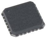
| 供应商器件封装 | 24-LFCSP-VQ(4x4) |
| 其它名称 | ADL5310ACPZ-REEL7DKR |
| 包装 | Digi-Reel® |
| 安装类型 | 表面贴装 |
| 封装/外壳 | 24-VFQFN 裸露焊盘,CSP |
| 应用 | 光纤 |
| 标准包装 | 1 |
| 类型 | 对数转换器 |
| 设计资源 |


- 商务部:美国ITC正式对集成电路等产品启动337调查
- 曝三星4nm工艺存在良率问题 高通将骁龙8 Gen1或转产台积电
- 太阳诱电将投资9.5亿元在常州建新厂生产MLCC 预计2023年完工
- 英特尔发布欧洲新工厂建设计划 深化IDM 2.0 战略
- 台积电先进制程称霸业界 有大客户加持明年业绩稳了
- 达到5530亿美元!SIA预计今年全球半导体销售额将创下新高
- 英特尔拟将自动驾驶子公司Mobileye上市 估值或超500亿美元
- 三星加码芯片和SET,合并消费电子和移动部门,撤换高东真等 CEO
- 三星电子宣布重大人事变动 还合并消费电子和移动部门
- 海关总署:前11个月进口集成电路产品价值2.52万亿元 增长14.8%


PDF Datasheet 数据手册内容提取
120 dB Range (3 nA to 3 mA) Dual Logarithmic Converter Data Sheet ADL5310 FEATURES FUNCTIONAL BLOCK DIAGRAM 2 independent channels optimized for photodiode interfacing 665kΩ VREF VRDZ 6-decade input dynamic range VSUM OUT1 Law conformance 0.3 dB from 3 nA to 3 mA COMM VOUT1 Ω Temperature-stable logarithmic outputs IRF1 4.99k Nominal slope 10 mV/dB (200 mV/dec), externally scalable SCL1 Intercepts may be independently set by external resistors VBIAS 6.69kΩ BIN1 USisnegrl-eco-snufpigpulyra obrl ed uoault-psuupt pbluyf foepre armatpiolinfi ers VNEG CTOEMMPPEENRSAATUTIROENILOG 451Ω LOG1 Space efficient, 24-lead 4 mm × 4 mm LFCSP 14.2kΩ Low power: <10 mA quiescent current IPD1 INP1 OUT2 0.5V 2.5V REFERENCE APPLICATIONS 20kΩ 80kΩ GENERATOR VOUT2 Ω Gain and absorbance measurements IRF2 COMM 4.99k Multichannel power monitoring SCL2 General-purpose baseband log compression VBIAS 14.2kΩ BIN2 VNEG CTOEMMPPEENRSAATUTIROENILOG 451Ω LOG2 6.69kΩ IPD2 INP2 COMM VSUM 665kΩ VREF 04415-0-001 Figure 1. GENERAL DESCRIPTION The ADL53101 low cost, dual logarithmic amplifier converts input VSUM potential. The VSUM potential is internally set to 500 mV current over a wide dynamic range to a linear-in-dB output but may be externally grounded for dual-supply operation, and voltage. It is optimized to determine the optical power in wide- for additional applications requiring voltage inputs. ranging optical communication system applications, including The logarithmic slope is set to 10 mV/dB (200 mV/decade) control circuitry for lasers, optical switches, atten-uators, and nominal and can be modified using external resistors and the amplifiers, as well as system monitoring. The device is equivalent independent buffer amplifiers. The logarithmic intercepts for to a dual AD8305 with enhanced dynamic range (120 dB). While each channel are defined by the individual reference currents, the ADL5310 contains two independent signal channels with which are set to 3 μA nominal for maximum input range by individually configurable transfer function constants (slope and connecting 665 kΩ resistors between the 2.5 V VREF pins and intercept), internal bias circuitry is shared between channels for the IRF1 and IRF2 inputs. Tying VRDZ to VREF effectively sets improved power consumption and channel matching. Dual the x-intercept four decades below the reference current, which converters in a single, compact LFCSP package yield space- is typically 300 pA for a 3 µA reference. efficient solutions for measuring gain or attenuation across The use of individually optimized reference currents may be optical elements. Only a single supply is required; optional valuable when using the ADL5310 for gain or absorbance measure- dual-supply operation offers added flexibility. ments where each channel input has a different current range The ADL5310 employs an optimized translinear structure that requirement. The reference current inputs are also fully functional use the accurate logarithmic relationship between a bipolar dynamic inputs, allowing log ratio operation with the reference transistor’s base emitter voltage and collector current, with input current as the denominator. The ADL5310 is specified for appropriate scaling by precision currents to compensate for the operation from –40°C to +85°C. inherent temperature dependence. Input and reference current pins sink current ranging from 3 nA to 3 mA (limited to ±60 dB between input and reference) into a fixed voltage defined by the 1 Protected by US Patents 4,604,532, and 5,519,308. Other patents pending. Rev. B Document Feedback Information furnished by Analog Devices is believed to be accurate and reliable. However, no responsibility is assumed by Analog Devices for its use, nor for any infringements of patents or other One Technology Way, P.O. Box 9106, Norwood, MA 02062-9106, U.S.A. rights of third parties that may result from its use. Specifications subject to change without notice. No license is granted by implication or otherwise under any patent or patent rights of Analog Devices. Tel: 781.329.4700 ©2003–2018 Analog Devices, Inc. All rights reserved. Trademarks and registered trademarks are the property of their respective owners. Technical Support www.analog.com
ADL5310 Data Sheet TABLE OF CONTENTS Features .............................................................................................. 1 Theory .......................................................................................... 11 Applications ....................................................................................... 1 Managing Intercept and Slope .................................................. 12 Functional Block Diagram .............................................................. 1 Response Time and Noise Considerations ............................. 12 General Description ......................................................................... 1 Applications Information .............................................................. 13 Revision History ............................................................................... 2 Calibration ................................................................................... 14 Specifications ..................................................................................... 3 Minimizing Crosstalk ................................................................ 14 Absolute Maximum Ratings ............................................................ 4 Relative and Absolute Power Measurements .......................... 15 ESD Caution .................................................................................. 4 Characterization Methods ........................................................ 16 Pin Configuration and Function Descriptions ............................. 5 Evaluation Board ............................................................................ 17 Typical Performance Characteristics ............................................. 6 Outline Dimensions ....................................................................... 20 General Structure ........................................................................... 11 Ordering Guide .......................................................................... 20 REVISION HISTORY 4/2018—Rev. A to Rev. B Changes to Figure 2 and Table 3 ..................................................... 5 Changes to Figure 40 ...................................................................... 18 Updated Outline Dimensions ....................................................... 20 Changes to Ordering Guide .......................................................... 20 9/2004—Rev. 0 to Rev. A Changes to Ordering Guide .......................................................... 20 11/2003—Revision 0: Initial Version Rev. B | Page 2 of 20
Data Sheet ADL5310 SPECIFICATIONS VP = 5 V, VN = 0 V, T = 25°C, R = 665 kΩ, and VRDZ connected to VREF, unless otherwise noted. A REF Table 1. Parameter Test Conditions/Comments Min Typ Max Unit INPUT INTERFACE Pin 1 to Pin 6: INP1 and INP2, IRF1 and IRF2, VSUM Specified Current Range, I Flows toward INP1 pin or INP2 pin 3 n 3 m A PD Input Current Min/Max Limits Flows toward INP1 pin or INP2 pin 10 m A Reference Current, I , Range Flows toward IRF1 pin or IRF2 pin 3 n 3 m A REF Summing Node Voltage Internally preset; user alterable 0.46 0.5 0.54 V Temperature Drift –40°C < T < +85°C 0.030 mV/°C A Input Offset Voltage VIN − VSUM, VIREF − VSUM −20 +20 mV LOGARITHMIC OUTPUTS Pin 15 and Pin 16: LOG1 and LOG2 Logarithmic Slope 190 200 210 mV/dec –40°C < T < +85°C 185 215 mV/dec A Logarithmic Intercept1 165 300 535 pA –40°C < T < +85°C 40 1940 pA A Law Conformance Error 10 nA < I < 1 mA 0.1 0.4 dB PD 3 nA < I < 3 mA 0.3 0.6 dB PD Wideband Noise2 I > 3 µA; output referred 0.5 µV/√Hz PD Small Signal Bandwidth2 I = 3 µA 1.5 MHz PD Maximum Output Voltage 1.7 V Minimum Output Voltage Limited by V = 0 V 0.10 V N Output Resistance 4.375 5 5.625 kΩ REFERENCE OUTPUT Pin 7 and Pin 24 (internally shorted): VREF Voltage wrt Ground 2.45 2.5 2.55 V –40°C < T < +85°C 2.42 2.58 V A Maximum Output Current Sourcing (grounded load) 20 mA Incremental Output Resistance Load current < 10 mA 4 Ω OUTPUT BUFFERS Pins 12 to 14 and 17 to 19: OUT2, SCL2, BIN2, BIN1, SCL1, and OUT1 Input Offset Voltage −20 +20 mV Input Bias Current Flowing out of Pins 13, 14, 17, and 18 0.4 µA Incremental Input Resistance 35 MΩ Incremental Output Resistance Load current < 10 mA; gain = 1 0.5 Ω Output High Voltage RL = 1 kΩ to ground VP − 0.1 V Output Low Voltage R = 1 kΩ to ground 0.10 V L Peak Source/Sink Current 30 mA Small-Signal Bandwidth Gain = 1 15 MHz Slew Rate 0.2 V to 4.8 V output swing 15 V/µs POWER SUPPLY Pins 8 and 9: VPOS; Pins 10, 11, and 20: VNEG Positive Supply Voltage (V – V ) ≤ 12 V 3 5 12 V P N Quiescent Current Input currents < 10 µA 9.5 11.5 mA Negative Supply Voltage (Optional) (VP – VN ) ≤ 12 V −5.5 0 V 1 Other values of logarithmic intercept can be achieved by adjustment of RREF. 2 Output noise and incremental bandwidth are functions of input current; measured using output buffer connected for GAIN = 1. Rev. B | Page 3 of 20
ADL5310 Data Sheet ABSOLUTE MAXIMUM RATINGS Stresses at or above those listed under Absolute Maximum Table 2. Ratings may cause permanent damage to the product. This is a Parameter Rating stress rating only; functional operation of the product at these Supply Voltage VP − VN 12 V or any other conditions above those indicated in the operational Input Current 20 mA section of this specification is not implied. Operation beyond Internal Power Dissipation 500 mW the maximum operating conditions for extended periods may θ 35°C/W1 JA affect product reliability. Maximum Junction Temperature 125°C ESD CAUTION Operating Temperature Range –40°C to +85°C Storage Temperature Range −65°C to +150°C Lead Temperature Range (Soldering 60 sec) 300°C 1 With paddle soldered down. Rev. B | Page 4 of 20
Data Sheet ADL5310 PIN CONFIGURATION AND FUNCTION DESCRIPTIONS FE ZD MM MM GE 1T R R O O N U V V C C V O 42 32 22 12 02 91 VSUM1 18SCL1 INP12 17BIN1 ADL5310 IRF13 16LOG1 DUAL LOG AMP IRF24 TOP VIEW 15LOG2 INP25 (Not to Scale) 14BIN2 VSUM6 13SCL2 7 8 9 0 1 2 1 1 1 F S S G G 2 ERV OPV OPV ENV ENV TUO N1.OEBVTXIEAEP C SAOO SLNEONDWE PC IAMTDEP.DE T DTHAOEN AECNXEAP POLAOSTGEHD .G PRAODU MNDUST 04415-0-002 Figure 2. 24-Lead LFCSP Pin Configuration Table 3. Pin Function Descriptions Pin No. Mnemonic Function 1, 6 VSUM Guard Pin. Used to shield the INP1 and INP2 input current lines, and for optional adjustment of the input summing node potentials. Pin 1 and Pin 6 are internally shorted. 2 INP1 Channel 1 Numerator Input. Accepts (sinks) photodiode current I . Usually connected to photodiode anode PD1 such that photocurrent flows into INP1. 3 IRF1 Channel 1 Denominator Input. Accepts (sinks) reference current, I . RF1 4 IRF2 Channel 2 Denominator Input. Accepts (sinks) reference current, I . RF2 5 INP2 Channel 2 Numerator Input. Accepts (sinks) photodiode current I . Usually connected to photodiode anode PD2 such that photocurrent flows into INP2. 7, 24 VREF Reference Output Voltage of 2.5 V. Pin 7 and Pin 24 are internally shorted. 8, 9 VPOS Positive Supply, (V – V ) ≤ 12 V. Both pins must be connected externally. P N 10, 11, 20 VNEG Optional Negative Supply, V . These pins are usually grounded. For more details, see the General Structure and N Applications Information sections. All VNEG pins must be connected externally. 12 OUT2 Buffer Output for Channel 2. 13 SCL2 Buffer Amplifier Inverting Input for Channel 2. 14 BIN2 Buffer Amplifier Noninverting Input for Channel 2. 15 LOG2 Output of the Logarithmic Front End for Channel 2. 16 LOG1 Output of the Logarithmic Front End for Channel 1. 17 BIN1 Buffer Amplifier Noninverting Input for Channel 1. 18 SCL1 Buffer Amplifier Inverting Input for Channel 1. 19 OUT1 Buffer Output for Channel 1. 21, 22 COMM Analog Ground. Pin 21 and Pin 22 are internally shorted. 23 VRDZ Intercept Shift Reference Input. The top of a resistive divider network that offsets VLOG to position the intercept. Normally connected to VREF; may also be connected to ground when bipolar outputs are to be provided. EPAD Exposed Pad. The exposed pad must be connected to analog ground via a low impedance path. Rev. B | Page 5 of 20
ADL5310 Data Sheet TYPICAL PERFORMANCE CHARACTERISTICS V = 5 V, V = 0 V, R = 665 kΩ, T = 25°C, unless otherwise noted. P N REF A 1.6 2.0 TA =–40°C, 0°C, +25°C, +70°C,+85°C VIN = 0V 1.4 1.5 1.2 1.0 +85°C dB)) +25°C +70°C V)1.0 mV/0.5 (G 10 LO0.8 B ( 0 V d R ( 0.6 O–0.5 ERR 0°C –40°C 0.4 –1.0 0.2 –1.5 01n 10n 100n 1µIINP (A)10µ 100µ 1m 10m 04415-0-003 –2.01n 10n 100n 1µIINP (A)10µ 100µ 1m 10m 04415-0-006 Figure 3. VLOG vs. IINP for Multiple Temperatures Figure 6. Law Conformance Error vs. IINP for Multiple Temperatures, Normalized to 25°C 1.8 2.0 TA =–40°C, 0°C, +25°C, +70°C,+85°C 1.6 VIN = 0V 1.5 1.4 1.0 1.2 dB)) +70°C +85°C V) mV/0.5 +25°C (G1.0 10 LO B ( 0 V0.8 R (d O–0.5 0.6 R R E –40°C 0°C –1.0 0.4 0.2 –1.5 01n 10n 100n 1µIREF (A1)0µ 100µ 1m 10m 04415-0-004 –2.01n 10n 100n 1µIREF (A1)0µ 100µ 1m 10m 04415-0-007 Figure 4. VLOG vs. IREF for Multiple Temperatures (IINP = 3 µA) Figure 7. Law Conformance Error vs. IREF for Multiple Temperatures, Normalized to 25°C (IINP = 3 µA) 1.8 1.0 1.6 0.8 3mA 1.4 3µA 0.6 300µA 30µA V)1.2 3nA30nA300nA mV/dB)) 00..24 3µA (G1.0 10 LO B ( 0 V0.8 OR (d –0.2 300nA 0.6 3mA R 300µA ER –0.4 0.4 30µA –0.6 0.2 –0.8 3nA 30nA 01n 10n 100n 1µIINP (A)10µ 100µ 1m 10m 04415-0-005 –1.01n 10n 100n 1µIINP (A)10µ 100µ 1m 10m 04415-0-008 Figure 5. VLOG vs. IINP for Multiple Values of IREF, Figure 8. Law Conformance Error vs. IINP for Multiple Values of IREF, Decade Steps from 3 nA to 3 mA Decade Steps from 3 nA to 3 mA Rev. B | Page 6 of 20
Data Sheet ADL5310 1.8 1.0 1.6 0.8 3nA 30nA 1.4 0.6 300nA (V)G11..02 30µA300µA3mA 10mV/dB)) 00..24 3µA 3µA LO B ( 0 V0.8 3nA OR (d –0.2 3mA 0.6 30nA300nA ERR –0.4 300µA 3mA 0.4 3µA –0.6 30µA 0.2 –0.8 01n 10n 100n 1µIREF (A1)0µ 100µ 1m 10m 04415-0-009 –1.01n 10n 100n 1µIREF (A1)0µ 100µ 1m 10m 04415-0-012 Figure 9. VLOG vs. IREF for Multiple Values of IINP, Figure 12. Law Conformance Error vs. IREF for Multiple Values of IINP, Decade Steps from 3 nA to 3 mA Decade Steps from 3 nA to 3 mA 1.0 2.0 TA = 25°C 0.8 1.5 +5V, 0V +12V, 0V 0.6 B))0.4 +12V, 0V B)) 1.0 mV/d0.2 +9V, 0V mV/d 0.5 MEAN + 3σ B (10 0 +3V, 0V B (10 0 ROR (d–0.2 +5V,–5V +5V,–5V ROR (d –0.5 MEAN– 3σ ER–0.4 ER –1.0 –0.6 –1.5 –0.8 –1.01n 10n 100n 1µIINP (A)10µ 100µ 1m 10m 04415-0-010 –2.01n 10n 100n 1µIPD (A)10µ 100µ 1m 10m 04415-0-013 Figure 10. Law Conformance Error vs. IINP for Various Supply Conditions Figure 13. Law Conformance Error Distribution (3σ to Either Side of Mean) 2.0 4 TA = 0°C, 70°C TA =–40°C, 85°C 1.5 3 MEAN + 3σ AT–40°C 1.0 MEAN + 3σ AT 70°C 2 B)) B)) d d V/ 0.5 V/ 1 m m 10 10 MEAN + 3σ AT +85°C B ( 0 MEAN± 3σ AT 0°C B ( 0 d d R ( R ( O –0.5 O –1 R R R R E E –1.0 MEAN– 3σ AT 70°C –2 –1.5 –3 MEAN– 3σ AT–40°C –2.01n 10n 100n 1µIPD (A)10µ 100µ 1m 10m 04415-0-011 –41n 10n 100n 1µIPD (A)10µ 100µ 1m 10m 04415-0-014 Figure 11. Law Conformance Error Distribution (3σ to Either Side of Mean) Figure 14. Law Conformance Error Distribution (3σ to Either Side of Mean) Rev. B | Page 7 of 20
ADL5310 Data Sheet 15 1.6 30nA 10 300nA 1.4 5 3nA dB) 0 30µA 1.2 T-RISE < 1µs T-FALL < 1µs 300µA TO 3mA SE ( –5 T-RISE < 1µs T-FALL < 1µs 30µA TO 300µA RESPON––1150 300µA (V)OUT01..80 T-RISE < 1µs T-FALL < 5µs 3µA TO 30µA ED –20 V T-RISE < 5µs T-FALL < 10µs 300nA TO 3µA MALIZ––2350 3mA 0.6 T-RISE < 10µs T-FALL < 40µs 30nA TO 300nA NOR–35 3µA 0.4 –40 T-RISE < 30µs T-FALL < 80µs 3nA TO 30nA 0.2 –45 –50100 1k 10kFREQU1E0N0kCY (Hz)1M 10M 100M 04415-0-015 00 20 40 60 80TIM1E0 0(µs)120 140 160 180 200 04415-0-018 Figure 15. Small Signal AC Response, IINP to VOUT (AV = 1) Figure 18. Pulse Response—IINP to VOUT (AV = 1) (5% Sine Modulation, Decade Steps from 3 nA to 3 mA) in Consecutive 1-Decade Steps 15 1.6 30nA 10 300nA 1.4 5 3mA dB) 0 1.2 T-RISE < 80µs T-FALL < 30µs 3nA TO 30nA RESPONSE (––1–1505 3nA 300µA (V)OUT01..80 TT--RRIISSEE << 1400µµss TT--FFAALLLL << 15µ0µss 33000nnAA T TOO 3 03µ0nAA ED –20 3µA V T-RISE < 1µs T-FALL < 1µs 3µA TO 30µA LIZ–25 0.6 MA–30 T-RISE < 1µs T-FALL < 1µs 30µA TO 300µA OR–35 30µA 0.4 N T-RISE < 1µs T-FALL < 1µs 300µA TO 3mA –40 0.2 –45 –50100 1k 10kFREQU1E0N0kCY (Hz)1M 10M 100M 04415-0-016 00 20 40 60 80TIM1E0 0(µs)120 140 160 180 200 04415-0-019 Figure 16. Small Signal AC Response, IREF to VOUT (AV = 1) Figure 19. Pulse Response—IREF to VOUT (AV = 1) (5% Sine Modulation, Decade Steps from 3 nA to 3 mA) in Consecutive 1-Decade Steps 100 5.0 3nA 4.0 10 30nA V rms/ Hz 1 300nA 3µA mVrms 3.0 µ 2.0 0.1 1.0 300µA 3mA 30µA 0.01100 1k F1R0EkQUENCY1 (0H0zk) 1M 10M 04415-0-017 01n 10n 100n 1µIINP (A1)0µ 100µ 1m 10m 04415-0-020 Figure 17. Spot Noise Spectral Density at VOUT vs. Frequency (AV = 1) Figure 20. Total Wideband Noise Voltage at VOUT vs. IINP (AV = 1) for IINP in Decade Steps from 3 nA to 3 mA Rev. B | Page 8 of 20
Data Sheet ADL5310 25 5 20 4 15 3 2 10 mV) 5 MEAN + 3σ mV) 1 MEAN + 3σ FT ( FT ( 0 RI 0 RI D D –1 MEAN– 3σ EF –5 PT VR MEAN– 3σ VIN –2 –10 –3 –15 –4 –20 –5 –25–40 –30 –20 –10 0 TE1M0PE2R0AT3U0RE 4(°0C) 50 60 70 80 90 04415-0-021 –6–40 –30 –20 –10 0 TE1M0PE2R0AT3U0RE 4(°0C) 50 60 70 80 90 04415-0-024 Figure 21. VREF Drift vs. Temperature (3σ to Either Side of Mean) Figure 24. VINPT Drift vs. Temperature (3σ to Either Side of Mean) Normalized to 25°C Normalized to 25°C 6 7 5 6 4 5 3 4 V DRIFT (mV/dec)Y ––20121 MEAN + 3σMEAN– 3σ ∆V DRIFT (mV/dec)Y ––131022 MEANM +E A3Nσ– 3σ –3 –3 –4 –4 –5 –5 –6–40 –30 –20 –10 0 TE1M0PE2R0AT3U0RE 4(°0C) 50 60 70 80 90 04415-0-022 –6–40 –30 –20 –10 0 TE1M0PE2R0AT3U0RE 4(°0C) 50 60 70 80 90 04415-0-025 Figure 22. Slope Drift vs. Temperature (3σ to Either Side of Mean) Figure 25. Slope Mismatch Drift vs. Temperature Normalized to 25°C (VY1 – VY2, 3σ to Either Side of Mean) Normalized to 25°C 200 200 150 150 100 100 pA) 50 MEAN + 3σ A) 50 MEAN + 3σ DRIFT ( 0 RIFT (p 0 I Z DZ –50 MEAN– 3σ MEAN– 3σ ∆I –50 –100 –100 –150 –150–40 –30 –20 –10 0 TE1M0PE2R0AT3U0RE 4(°0C) 50 60 70 80 90 04415-0-023 –200–40 –30 –20 –10 0 TE1M0PE2R0AT3U0RE 4(°0C) 50 60 70 80 90 04415-0-026 Figure 23. Intercept Drift vs. Temperature Figure 26. Intercept Mismatch Drift vs. Temperature (3σ to Either Side of Mean) Normalized to 25°C (IZ1 – IZ2, 3σ to Either Side of Mean) Normalized to 25°C Rev. B | Page 9 of 20
ADL5310 Data Sheet 700 450 400 600 350 500 300 NT 400 NT 250 U U O O C 300 C 200 150 200 100 100 50 0190 195 SLOPE2 0(m0V/dec) 205 210 04415-0-027 0–9 –6 SL–O3PE MISMA0TCH (mV/3dec) 6 9 04415-0-030 Figure 27. Distribution of Logarithmic Slope Figure 30. Distribution of Channel-to-Channel Slope Mismatch (VY1 – VY2) 600 500 500 400 400 300 NT NT OU 300 OU C C 200 200 100 100 0100 200 INTER3C0E0PT (pA) 400 500 04415-0-028 0–300 –200 IN–T1E0R0CEPT M0ISMATCH1 0(p0A) 200 300 04415-0-031 Figure 28. Distribution of Logarithmic Intercept Figure 31. Distribution of Channel-to-Channel Intercept Mismatch (IZ1 – IZ2) 700 500 600 400 500 300 NT 400 NT U U O O C 300 C 200 200 100 100 02.46 2.48 VREF V2O.5L0TAGE (V) 2.52 2.54 04415-0-029 0–9 –6 VIN–P3T– VSUM V0OLTAGE 3(mV) 6 9 04415-0-032 Figure 29. Distribution of VREF (RL = 100 kΩ) Figure 32. Distribution of Offset Voltage (VINPT – VSUM) Rev. B | Page 10 of 20
Data Sheet ADL5310 GENERAL STRUCTURE The ADL5310 addresses a wide variety of interfacing conditions THEORY to meet the needs of fiber optic supervisory systems and is useful The base-emitter voltage of a bipolar junction transistor (BJT) in many nonoptical applications. These notes explain the structure can be expressed by Equation 1, which immediately shows its of this unique style of translinear log amp. Figure 33 shows the basic logarithmic nature: key elements of one of the two identical on-board log amps. V = kT/q ln(I /I) (1) BE C S BIAS where: GENERATOR I is the collector current. PHOINTOPUDTIODE2.5V VREF IREF VBE1 CTOEMMPPEENRSAATUTIROEN ICS is a scaling current, typically only 10–17 A. CURRENT80kΩ IREF VBE2 (SUBTRACT AND kT/q is the thermal voltage, proportional to absolute 20kΩ DIVIDE BY T°K) IPD 0.5V COMM temperature (PTAT), and is 25.85 mV at 300 K. INP1 VSUM 0.5V 44µA/dec IS is never precisely defined and exhibits an even stronger temper- (INP2) ature dependence, varying by a factor of roughly a billion between 14.2kΩ 451Ω VRDZ −35°C and +85°C. Thus, to make use of the BJT as an accurate VLOG 0.5V logarithmic element, both of these temperature dependencies Q1 VBE1 Q2 VBE2 6.69kΩ must be eliminated. VNEG (NORMALLY GROUNDED) COMM 04415-0-033 Tpahier dofif BfeJrTesn, coen bee otwpeereant itnhge abta tshee- epmhoitttoedr ivoodltea cguesr roefn at ImPDa tacnhde d Figure 33. Simplified Schematic of Single Log Amp the other operating at a reference current I , can be written as REF The photodiode current IPD is received at either Pin INP1 or VBE1 – VBE2 = kT/q ln(IPD/IS) – kT/q ln(IREF/IS) Pin INP2. The voltages at these nodes are approximately equal = ln(10) kT/q log10(IPD/IREF) (2) to the voltage on the adjacent guard pins, VSUM, as well as reference = 59.5 mV log10(IPD/IREF) (T = 300 K) inputs IRF1 and IRF2, due to the low offset voltage of the JFET The uncertain, temperature-dependent saturation current, I, S operational amplifiers. Transistor Q1 converts IPD to a corre- that appears in Equation 1 has therefore been eliminated. To sponding logarithmic voltage, as shown in Equation 1. A finite eliminate the temperature variation of kT/q, this difference positive value of VSUM is needed to bias the collector of Q1 for voltage is processed by what is essentially an analog divider. the usual case of a single-supply voltage. This is internally set to Effectively, it puts a variable under Equation 2. The output of 0.5 V, one-fifth of the 2.5 V reference voltage that appears on this process, which also involves a conversion from voltage Pin VREF. Both VREF pins are internally shorted, as are both mode to current mode, is an intermediate, temperature- VSUM pins. The resistance at the VSUM pin is nominally 16 kΩ; corrected current: this voltage is not intended as a general bias source. I = I log (I /I ) (3) LOG Y 10 PD REF The ADL5310 also supports the use of an optional negative supply where I is an accurate, temperature-stable scaling current that Y voltage, V , at Pin VNEG. When V is 0.5 V or more negative, N N determines the slope of the function (change in current per VSUM may be connected to ground; thus, INP1, INP2, IRF1, decade). and IRF2 assume this potential. This allows operation as a voltage- input logarithmic converter by the inclusion of a series resistor For the ADL5310, IY is 44 µA, resulting in a temperature- at either or both inputs. Note that the resistor setting IREF for independent slope of 44 µA/decade for all values of IPD and IREF. each channel needs to be adjusted to maintain the intercept value. This current is subsequently converted back to a voltage-mode Also, note that the collector-emitter voltages of Q1 and Q2 are output, VLOG, scaled 200 mV/decade. the full VN and effects due to self-heating cause errors at large It is apparent that this output is 0 for IPD = IREF and must swing input currents. negative for smaller values of input current. To avoid this, I REF The input-dependent VBE1 of Q1 is compared with the reference would need to be as small as the smallest value of IPD. Accordingly, VBE2 of a second transistor, Q2, operating at IREF. IREF is generated an offset voltage is added to VLOG to shift it upward by 0.8 V when externally to a recommended value of 3 µA. However, other VRDZ is directly connected to VREF. This moves the intercept values over a several-decade range can be used with a slight to the left by four decades (at 200 mV/decade), from 3 μA to degradation in law conformance. 300 pA: I = I log (I /I ) (4) LOG Y 10 PD INTC where I is the operational value of the intercept current. INTC Rev. B | Page 11 of 20
ADL5310 Data Sheet Because values of I < I result in a negative V , a negative Thus, the effective intercept current I is only one ten- PD INTC LOG INTC supply of sufficient value is required to accommodate this thousandth of I , corresponding to 300 pA when using the REF situation. recommended value of I = 3 μA. REF The voltage V is generated by applying I to an internal The slope can be reduced by attaching a resistor between the log LOG LOG resistance of 4.55 kΩ, formed by the parallel combination of a amp output pin, LOG1 or LOG2, and ground. This is strongly 6.69 kΩ resistor to ground and a 14.2 kΩ resistor to Pin VRDZ discouraged given that the on-chip resistors do not ratio (typically tied to the 2.5 V reference, VREF). At the LOG1 correctly to the added resistance. In addition, it is rare that one (LOG2) pin, the output current I generates a voltage of would wish to lower the basic slope of 10 mV/dB; if this is LOG needed, it should be effected at the low impedance output of the V = I × 4.55 kΩ LOG LOG buffer amps, which are provided to avoid such miscalibration = 44 μA × 4.55 kΩ × log (I /I ) (5) 10 PD INTC and to allow higher slopes to be used. = V log (I /I ) Y 10 PD INTC Each buffer of the ADL5310 is essentially an uncommitted where V = 200 mV/decade or 10 mV/dB. Y operational amplifier with rail-to-rail output swing, good load Note that any resistive loading on LOG1 (LOG2) lowers this driving capabilities, and a typical unity-gain bandwidth of 15 MHz. slope and results in an overall scaling uncertainty. This is due to In addition to allowing the introduction of gain, using standard the variability of the on-chip resistors compared to the off-chip feedback networks and thereby increasing the slope voltage V , Y load. As a consequence, this practice is not recommended. the buffer can be used to implement multipole, low-pass filters, VLOG may also swing below ground when dual supplies (VP and threshold detectors, and a variety of other functions. Further VN) are used. When VN = −0.5 V or larger, the input Pins INP1 details on these applications can be found in the AD8304 data (INP2) and IRF1 (INP2) may be positioned at ground level sheet. simply by grounding VSUM. Care must be taken to limit the RESPONSE TIME AND NOISE CONSIDERATIONS power consumed by the input BJT devices when using a larger negative supply, because self heating degrades the accuracy at The response time and output noise of the ADL5310 are funda- higher currents. mentally a function of the signal current, IPD. For small currents, the bandwidth is proportional to I , as shown in Figure 15. The MANAGING INTERCEPT AND SLOPE PD output low frequency voltage-noise spectral-density is a function When using a single supply, VRDZ should be directly connected of I (see Figure 17) and increases for small values of I . Details PD REF to VREF to allow operation over the entire 6-decade input current of the noise and bandwidth performance of translinear log amps range. As noted in the Theory section, this introduces an accurate can be found in the AD8304 data sheet. offset voltage of 0.8 V at the LOG1 and LOG2 pins, equivalent to four decades, resulting in a logarithmic transfer function that can be written as V = V log (104 × I /I ) = V log (I /I ) (6) LOG Y 10 PD REF Y 10 PD INTC where I = I /104. INTC REF Rev. B | Page 12 of 20
Data Sheet ADL5310 APPLICATIONS INFORMATION 5V 665kΩ VSUM VREF VRDZ VPOS OUT1 0.5log10( I1 Pn D A1 ) COMM VOUT1 IRF1 12kΩ IRF1 SCL1 2kΩ 8kΩ 6.69kΩ 4.7nF BIN1 VBIAS TEMPERATURE ILOG LOG1 VNEG COMPENSATION 451Ω CFLT1 10 nF 14.2kΩ IPD1 INP1 1kΩ OUT2 0.5log10( I1 Pn D A2 ) 1nF 20kΩ 0.5V80kΩ 2.5V GREENFEERREANTCOER VOUT2 12kΩ COMM IRF2 SCL2 8kΩ 2kΩ 14.2kΩ 4.7nF BIN2 VBIAS TEMPERATURE ILOG LOG2 VNEG COMPENSATION 451Ω CFLT2 IRF2 10 nF 6.69kΩ IPD2 COMM INP2 1kΩ VSUM 11nnFF 665kΩ VREF VNEG COMM 04415-0-034 Figure 34. Basic Connections for Fixed Intercept Use The ADL5310 is easy to use in optical supervisory systems and in In addition, each input and reference pin (INP1, INP2, IRF1, similar situations where a wide-ranging current is to be converted and IRF2) has a compensation network made up of a series to its logarithmic equivalent, that is, represented in decibel terms. resistor and capacitor. The junction capacitance of the photo- Basic connections for measuring a single current at each input diode along with the network capacitance of the board artwork are shown in Figure 34, which also includes various nonessential around the input system creates a pole that varies widely with components, as explained next. input current. The RC network stabilizes the system by simul- taneously reducing this pole frequency and inserting a zero to The 2 V difference in voltage between the VREF and Input Pins compensate an additional pole inherent in the input system. In INP1 and INP2, in conjunction with the external 665 kΩ resistors general, the 1 nF, 1 kΩ network handles almost any photodiode R and R , provides 3 µA reference currents I and I into RF1 RF2 RF1 RF2 interface. In situations where larger active area photodiodes are Pins IRF1 and IRF2. Connecting VRDZ to VREF raises the used, or when long input traces are used, the capacitor value may voltage at LOG1 and LOG2 by 0.8 V, effectively lowering each need to be increased to ensure stability. Although the signal and intercept current I by a factor of 104 to position it at 300 pA. INTC reference input systems are similar, additional care is required A wide range of other values for I , from 3 nA to 3 mA, may REF to ensure stable operation of the reference inputs at temperature be used. The effect of such changes is shown in Figure 5 and extremes across the full current range of I (I ). It is recom- Figure 8. RF1 RF2 mended that filter components of 4.7 nF and 2 kΩ should be Any temperature variation in R (R ) must be taken into account RF1 RF2 used from Pin IRF1 (IRF2) to ground. Temperature-stable compo- when estimating the stability of the intercept. Also, the overall nents should always be used in critical locations, such as the noise increases when using very low values of I (I ). In fixed RF1 RF2 compensation networks. Y5V-type chip capacitors are to be intercept applications, there is little benefit in using a large reference avoided due to their poor temperature stability. current, because doing so only compresses the low current end The optional capacitor from LOG1 (LOG2) to ground forms a of the dynamic range when operated from a single supply. The single-pole, low-pass filter in combination with the 5 kΩ resis- capacitor between VSUM and ground is strongly recommended tance at this pin. For example, when using a C of 10 nF, the to minimize the noise on this node, to reduce channel-to-channel FLT 3 dB corner frequency is 3.2 kHz. Such filtering is useful in crosstalk, and to help provide clean reference currents. Rev. B | Page 13 of 20
ADL5310 Data Sheet minimizing the output noise, particularly when I is small. Figure 35 shows the improvement in accuracy when using a PD Multipole filters are more effective in reducing the total noise; 2-point calibration method. To perform this calibration, apply examples are provided in the AD8304 data sheet. two known currents, I and I, in the linear operating range 1 2 between 10 nA and 1 mA. Measure the resulting output, V and Because the basic scaling at LOG1 (LOG2) is 0.2 V/decade, and 1 V, respectively, and calculate the slope m and the intercept b: a 4 V swing at the buffer output would correspond to 20 decades, 2 it is often useful to raise the slope to make better use of the rail- m = (V – V)/[log (I) – log (I)] (7) 1 2 10 1 10 2 to-rail voltage range. For illustrative purposes, both channels in b = V – m × log (I) (8) 1 10 1 Figure 34 provide a 0.5 V/decade overall slope (25 mV/dB). The same calibration can be performed with two known optical Thus, using I = 3 μA, V runs from 0.2 V at I = 3 nA to REF LOG PD powers, P and P. This allows for calibration of the entire 1.4 V at I = 3 mA; the buffer output runs from 0.5 V to 3.5 V, 1 2 PD measurement system while providing a simplified relationship corresponding to a dynamic range of 120 dB (electrical, that is, between the incident optical power and V voltage: 60 dB optical power). LOG m = (V – V)/(P – P) (9) Further information on adjusting the slope and intercept, using 1 2 1 2 a negative supply, and additional operations can be found in the b = V1 – m × P1 (10) AD8305 data sheet. The uncalibrated error line in Figure 35 was generated assuming CALIBRATION that the slope of the measured output was 200 mV/decade when in fact it was actually 194 mV/decade. Correcting for this discre- Each channel of the ADL5310 has a nominal slope and intercept pancy decreased measurement error up to 3 dB. at LOG1 (LOG2) of 200 mV/decade and 300 pA, respectively, when configured as shown in Figure 34. These values are MINIMIZING CROSSTALK untrimmed and the slope alone may vary by as much as 7.5% Combining two high-dynamic-range logarithmic converters in over temperature. For this reason, it is recommended that a one IC carries potential pitfalls concerning channel-to-channel simple calibration be done to achieve increased accuracy. While isolation. Special care must be taken in several areas to ensure the ADL5310 offers improved slope and intercept matching acceptable crosstalk performance, particularly when one or compared to a randomly selected pair of AD8305 log amps, the both channels may operate at very low input currents. Fastidious specified accuracy can only be achieved by calibrating each supply bypassing, which is also necessary for overall stability, channel individually. and careful board layout are important first steps for 1.4 4 minimizing crosstalk. While the shared bias circuitry improves channel-to-channel 1.2 UNCALIBRATED ERROR 3 matching and reduces power consumption, it is also a source of 1.0 2 B)) crosstalk that must be mitigated. The VSUM pins, which are inter- d V/ nally shorted, should be bypassed with at least 1 nF to ground, V(V)LOG00..86 MEASURED OUTPUT 10 R (dB (10m a(<n3d0 2 n0A n)F. VisS rUecMom ism oef npdaertdi cfuolra or pimerpatoirotna nact et hbee cloauwsees ti tc aucrtrse anst sa O reference voltage input for each input system, but without the R 0.4 CALIBRATED ERROR –1 ER bandwidth limitation at low currents that the primary inputs incur. Disturbances at the VSUM pin that are well within the bandwidth 0.2 IDEAL OUTPUT –2 of the input are tracked by the loop and do not generate distur- 01n 10n 100n 1µIPD (A)10µ 100µ 1m 10m–3 04415-0-035 biInRa nFrec2fe)e.sr eatn tchee c ouurtrpeuntt s( acsaidues efdro bmy tvhoel tgaegnee vraalrlyia mtioinnosr a pt eIrRtuFr1b aantidon Figure 35. Using 2-Point Calibration to Increase Measurement Accuracy For this reason, the pole frequency at VSUM, which has a 16 kΩ typical source resistance, should be set below the minimum input system bandwidth for the lowest input current to be encountered. Because the low frequency noise at VSUM is also tracked by the loop within its available bandwidth, this is also a criterion for reducing the noise contribution at the output from the thermal noise of the 16 kΩ source resistance at VSUM. Rev. B | Page 14 of 20
Data Sheet ADL5310 A 10 nF capacitor on each VSUM pin (20 nF parallel equivalent) voltage, followed by differencing of the two signal levels in the combined with the 16 kΩ source resistance yields a 500 Hz pole, digital domain for a relative gain or absorbance measurement. which is sufficiently below the bandwidth for the minimum A more straightforward analog implementation includes the use input current of 3 nA. of a current mirror, as shown in Figure 37. The current mirror is used to feed an opposite polarity replica of the cathode photo- Residual crosstalk disturbance is particularly problematic at the current of PD2 into Channel 2 of the ADL5310. This allows one lowest currents for two reasons. First, the loop is unable to reject channel to be used as an absolute power meter for the optical summing node disturbances beyond the limited bandwidth. signal incident on PD2, while the opposite channel is used to Second, the settling response at the lowest currents to any residual directly compute the log ratio of the two input signals. disturbance is significantly slower than that for input currents even one or two decades higher (see Figure 18). 5V 5V 12 1.2 0.1µF VSUM VPOS OUT2 Φ2* ACTIVE CHANNEL OUTPUT PULSE, 1-DECADE STEP ADL5310 COMM 3µA TO 30µA 1nF V) 9 1.0 UT (m UT (V) *Φ2(V)≅0.2log10(10II0Np2A) L OUTP 6 IINP– 3nA 0.8 L OUTP IIN2=1kIPΩD2 INP2 log SBCINL22 NNE 3 IINP– 10nA IINP– 100nA 0.6 NNE 4.7nF TEMPERATURE ILOG2 LOG2 A A H H COMPENSATION C C 1nF E 0 0.4 E V V INACTI –3 IINP– 30nA 0.2 ACTI 2MΩ IRF2 log INACTIVE CHANNEL RESPONSE VRDZ OUT1 α21** 1kΩ BIAS Fi–g6u0re 36. Cross0t.a5lk Pulse R1e.0sTpIoMnEs (em fso)1r .V5arious Inp2.u0t Current2 V.5a0lues 04415-0-036 4.7nF VREF **α21(V)G≅E0N.2ElRogA1T0O(IRIPIND12) IPD2 IRF1 SCL1 log Figure 36 shows the measured response of an inactive channel PD2 InGaAs PIN 1kΩ BIN1 (dc input) to a 1-decade current step on the input of the active 4.7nF TEMPERATURE ILOG1 LOG1 channel for several inactive channel dc current values. Additional COMPENSATION system considerations may be necessary to ensure adequate 5V PD1 1nF settling time following a known transient when one or both InGaAs PIN IIN1 log INP1 channels are operating at very low input currents. 1kΩ COMM 0.1µF 4.7nF VSUM RMEELAASTUIVREE MANENDT ASB SOLUTE POWER 1nF VNEG COMM 04415-0-037 When properly calibrated, the ADL5310 provides two independent Figure 37. Absolute and Relative Power Measurement Application Using Modified Wilson Current Mirror channels capable of accurate absolute optical power measurements. Often, it is desirable to measure the relative gain or absorbance The presented current mirror is a modified Wilson mirror. Other across an optical network element, such as an optical amplifier current mirror implementations would also work, though the or variable attenuator. If each channel has identical logarithmic modified Wilson mirror provides fairly constant performance slopes and intercepts, this can easily be done by differencing the over temperature. It is essential to use matched pair transistors output signals of each channel. In reality, channel mismatch can when designing the current mirror to minimize the effects of result in significant errors over a wide range of input levels if temperature gradients and beta mismatch. left uncompensated. Postprocessing of the signal can be used to account for individual channel characteristics. This requires a simple calculation of the expected input level for a measured log Rev. B | Page 15 of 20
ADL5310 Data Sheet The solution in Figure 37 is no longer subject to potential channel CHARACTERIZATION METHODS mismatch issues. Individual channel slope and intercept charac- During the characterization of the ADL5310, the device was teristics can be calibrated independently. The accuracy was verified treated as a precision current-input logarithmic converter, because using a pair of calibrated current sources. The performance of it is impractical to generate accurate photocurrents by illumin- the circuit depicted in Figure 37 is shown in Figure 38 and ating a photodiode. The test currents were generated by using Figure 39. Multiple transfer functions and error plots are provided either a well calibrated current source, such as the Keithley 236, for various power levels. The accuracy is better than 0.1 dB over or a high value resistor from a voltage source to the input pin. a 5-decade range. The dynamic range is slightly reduced for strong Great care is needed when using very small input currents. For I input currents. This is due to the limited available swing of IN example, the triax output connection from the current generator the VLOG pin and can be recovered through careful selection was used with the guard tied to VSUM. The input trace on the of input and output optical tap coupling ratios. PC board was guarded by connecting adjacent traces to VSUM. 1.8 These measures are needed to minimize the risk of leakage current 1.6 paths. With 0.5 V as the nominal bias on the INP1 (INP2) pin, a φ2 WHENIPD1 = 100µA 1.4 leakage-path resistance of 1 GΩ to ground would subtract 0.5 nA V) from the input, which amounts to a −1.6 dB error for a 3 nA source E ( 1.2 G current. Additionally, the very high sensitivity at the input pins TA 1.0 α21 FOR MULTIPLE VALUES OF IPD1 L and the long cables commonly needed during characterization O V T 0.8 allow 60 Hz and RF emissions to introduce substantial measure- U UTP 0.6 ment errors. Careful guarding techniques are essential to reducing O the pickup of these spurious signals. 0.4 Additional information, including test setups, can be found in 0.2 the AD8305 and ADL5306 data sheets. –020 –10 0 LO10G10 [IPD201/IPD2] 3(d0B) 40 50 60 04415-0-038 Figure 38. Absorbance and Absolute Power Transfer Functions for Wilson Mirror ADL5310 Combination 0.5 0.4 0.3 IPD1=1µA 0.2 B) 0.1 d OR ( 0 R ER–0.1 IPD1=10µA –0.2 –0.3 IPD1= 100µA –0.4 –0.–540 –30 –20 –10LOG010 [IPD110/IPD22] 0(dB)30 40 50 60 04415-0-039 Figure 39. Log Conformance for Wilson Mirror ADL5310 Combination, Normalized to 10 mA Channel 1 Input Current, IIN1 Rev. B | Page 16 of 20
Data Sheet ADL5310 EVALUATION BOARD An evaluation board is available for the ADL5310 (Figure 40 shows the schematic). It can be configured for a wide variety of experiments. The gain of each buffer amp is factory-set to unity, providing a slope of 200 mV/dec, and the intercept is set to 300 pA. Table 4 describes the various configuration options. Table 4. Evaluation Board Configuration Options Component Function Default Condition P1 Supply Interface. Provides access to the Supply Pins VNEG, COMM, and P1 = installed VPOS. P2, R1, R3, R8, R9, Monitor Interface. By adding 0 Ω resistors to R1, R3, R8, R9, R17, R22, and P2 = not installed R17, R22, R25, R30 R25, the VRDZ, VREF, VSUM, BIN1, BIN2, OUT1, and OUT2 pin voltages R1 = R3 = R8 = open (size 0402) can be monitored using a high impedance probe. VBIAS allows for the R9 = R17 = open (size 0402) external bias voltages to be applied to J1 and J2. If R30 = 0 Ω, R22 = R25 = R30 = open (size 0402) VBIAS = VREF. R5, R6, R7, R16, Buffer Amplifier/Output Interface. The logarithmic slopes of the ADL5310 R5 = R19 = 0 Ω (size 0402) R18, R19, R20, can be altered using each buffer’s gain-setting resistors, R5 and R6, and R7 = R16 = 0 Ω (size 0402) R21, R31, R32, C4, R18 and R19. R7, R16, R31, R32, C19, and C20 allow for variation in the R20 = R21 = 0 Ω (size 0402) C14, C15, C16, buffer loading. R20, R21, C4, C14, C15, and C16 are provided for a variety R6 = R18 = open (size 0402) C19, C20 of filtering applications. R31 = R32 = open (size 0402) C4 = C14 = open (size 0402) C19 = C20 = open (size 0402) C15 = C16 = open (size 0402) LOG1 = OUT1 = installed LOG2 = OUT2 = installed R2, R28, R29 Intercept Adjustment. The voltage dropped across Resistors R28 and R29 R28 = R29 = 665 kΩ (size 0402) determines the intercept reference current for each log amp, nominally R2 = 0 Ω (size 0402) set to 3 µA using a 665 kΩ 1% resistor. R2 can be used to adjust the output offset voltage at the LOG1 and LOG2 outputs. R4, R10, R11, C2, Supply Decoupling. C2 = C5 = C9 = 100 pF (size 0402) C3, C5, C6, C8, C9 C3 = C6 = C8 = 0.01 µF (size 0402) R4 = R10 = R11 = 0 Ω (size 0402) C1, C7 Filtering VSUM. C1 = C7 = 0.01 µF (size 0402) R12, R13, R14, Input Compensation. Provides essential HF compensation at the Input R12 = R15 = 1 kΩ (size 0402) R15, C10, C11, Pins INP1, INP2, IRF1, and IRF2. R13 = R14 = 2 kΩ (size 0402) C12, C13 C10 = C13 = 1 nF (size 0402) C11 = C12 = 4.7 nF (size 0402) IREF, INPT Input Interface. The test board is configured to accept current through the IREF = INPT = installed SMA connectors labeled INP1 and INP2. Through-holes are provided to connect photodiodes in place of the INP1 and INP2 SMAs for optical interfacing. By removing R28 (R29 for INP2), a second current can be applied to the IRF1 (IRF2 for INP2) input (also SMA) for evaluating the ADL5310 in log ratio applications. J1, J2 SC-Style Photodiode. Provides for the direct mounting of SC-style J1 = J2 = open photodiodes. Rev. B | Page 17 of 20
ADL5310 Data Sheet VRDZ VNEG R7 0Ω OUT1 R3 C3 0.01µF R32 C20 3 OPEN OPEN OPEN R2 R4 J2 2 VBIAS 0Ω 0Ω R8 OPEN PHOTODIODE 1 C2 OUT1 C4 OPEN 100pF C1 0.01µF R5 0Ω R28 R29 665kΩ 665kΩ 24 23 22 21 20 19 C16 R1 VREF VRDZ COMM COMM VNEG OUT1 R6 OPEN R02Ω0 R02Ω4 LOG1 VSUM 1 VSUM SCL1 18 OPEN OPEN INP1 2 INP1 BIN1 17 LOG1 R26 0Ω R25 3 IRF1 LOG1 16 BIN1 IRF1 4 IRF2 ADL5310 LOG2 15 R27 0Ω OPEN LOG2 R21 R22 5 INP2 BIN2 14 BIN2 IRF2 R18 C14 C15 0Ω OPEN INP2 6 VSUMVREF VPOS VPOS VNEG VNEG OUT2SCL2 13 ORP19EN OPEN OPEN R02Ω3 LOG2 0Ω 7 8 9 10 11 12 R1k1Ω5 R2k1Ω4 R2k1Ω3 R1k1Ω2 VREF R9 OUT1 1 C13 C12 C11 C10 OPEN C5 100pF C9 100pF R17 BIN1 2 OPEN 1nF 4.7nF4.7nF 1nF R10 R11 OUT2 LOG1 3 0Ω 0Ω C6 0.01µF C8 0.01µF R16 0Ω OUT2 LOG2 4 3 R31 C19 J1 2 VBIAS OPEN OPEN BIN2 5 PHOTODIODE 1 AGND OUT2 6 C7 0.01µF VPOS 1 2 3 VNEG VREF 7 P1 VBIAS R30 OPEN P82 04415-0-040 Figure 40. Evaluation Board Schematic Rev. B | Page 18 of 20
Data Sheet ADL5310 04415-0-041 04415-0-042 Figure 41. Component-Side Layout Figure 42. Component-Side Silkscreen Rev. B | Page 19 of 20
ADL5310 Data Sheet OUTLINE DIMENSIONS DETAIL A (JEDEC 95) 4.10 0.30 4.00 SQ 0.25 PIN 1 3.90 0.20 INDICATOR 19 24 PININD I1CATOR AREA OPTIONS 18 1 (SEE DETAIL A) 0.50 BSC 2.20 EXPPAODSED 2.10 SQ 2.00 13 6 0.50 12 7 0.20 MIN TOP VIEW 0.40 BOTTOM VIEW 0.30 FOR PROPER CONNECTION OF 0.80 THE EXPOSED PAD, REFER TO 0.75 SIDE VIEW THE PIN CONFIGURATION AND 0.70 0.05 MAX FUNCTION DESCRIPTIONS 0.02 NOM SECTION OF THIS DATA SHEET. COPLANARITY SEATING 0.08 PLANE 0.203 REF PKG-004714 COMPLIANTTOJEDEC STANDARDS MO-220-WGGD-8. 10-19-2017-B Figure 43. 24-Lead Lead Frame Chip Scale Package [LFCSP] 4 mm × 4 mm Body and 0.75 mm Package Height (CP-24-10) Dimensions shown in millimeters ORDERING GUIDE Model Temperature Range Package Description Package Option ADL5310ACPZ-REEL7 –40°C to +85°C 24-Lead Lead Frame Chip Scale Package [LFCSP] CP-24-10 ADL5310-EVALZ Evaluation Board ©2003–2018 Analog Devices, Inc. All rights reserved. Trademarks and registered trademarks are the property of their respective owners. D04415-0-4/18(B) Rev. B | Page 20 of 20
Mouser Electronics Authorized Distributor Click to View Pricing, Inventory, Delivery & Lifecycle Information: A nalog Devices Inc.: ADL5310ACPZ-REEL7