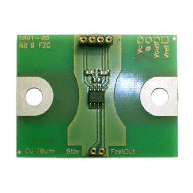
ICGOO在线商城 > 开发板,套件,编程器 > 评估板 - 传感器 > ADIS16407/PCBZ

 Datasheet下载
- 型号: ADIS16407/PCBZ
- 制造商: Analog
- 库位|库存: xxxx|xxxx
- 要求:
| 数量阶梯 | 香港交货 | 国内含税 |
| +xxxx | $xxxx | ¥xxxx |
查看当月历史价格
查看今年历史价格
ADIS16407/PCBZ产品简介:
ICGOO电子元器件商城为您提供ADIS16407/PCBZ由Analog设计生产,在icgoo商城现货销售,并且可以通过原厂、代理商等渠道进行代购。 ADIS16407/PCBZ价格参考。AnalogADIS16407/PCBZ封装/规格:评估板 - 传感器, ADIS16407 iMEMS®, iSensor™ Accelerometer, Barometric Pressure, Gyroscope, Magnetometer, 9 Axis Sensor Evaluation Board。您可以下载ADIS16407/PCBZ参考资料、Datasheet数据手册功能说明书,资料中有ADIS16407/PCBZ 详细功能的应用电路图电压和使用方法及教程。
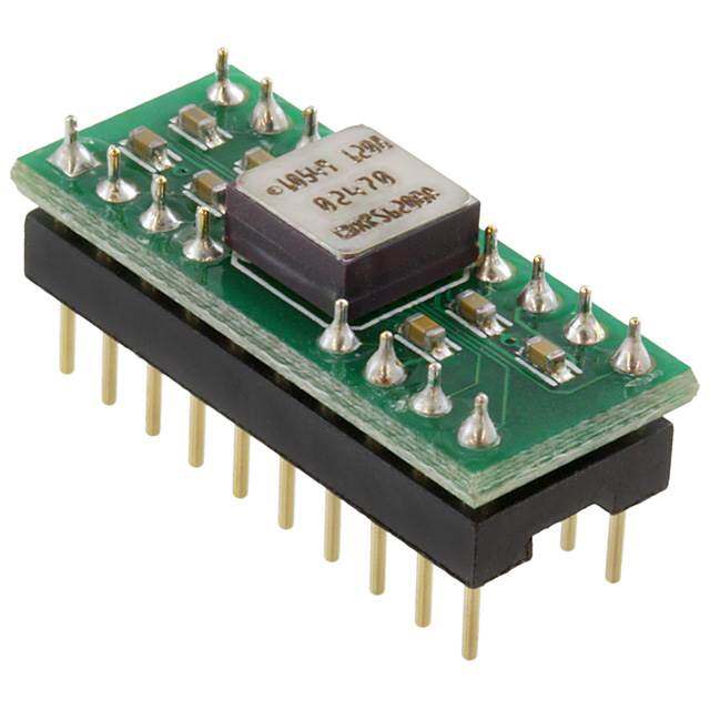
ADIS16407/PCBZ是Analog Devices Inc.推出的一款基于ADIS16407高性能惯性测量单元(IMU)的评估板,主要用于传感器系统的开发与测试。该评估板集成了三轴陀螺仪、三轴加速度计,具备高精度、低噪声和出色的温度稳定性,适用于对运动感知要求较高的应用场景。

典型应用包括工业自动化中的设备状态监测与振动分析,无人机和无人地面车辆的姿态控制与导航系统,以及机器人领域的运动反馈控制。此外,该评估板也广泛用于精密仪器、平台稳定系统(如云台和天线稳定装置)和结构健康监测等领域。

由于其即插即用的设计和配套的软件工具(如ADI的IMU Evaluation Software),ADIS16407/PCBZ便于工程师快速评估传感器性能、采集数据并进行算法开发,显著缩短产品开发周期。其坚固的设计也适合在复杂电磁环境或振动较强的工业现场使用。

总之,ADIS16407/PCBZ是一款面向高端运动传感应用的实用化评估平台,适用于需要高可靠性与精确动态测量的科研、工业及嵌入式系统开发场景。
| 参数 | 数值 |
| 产品目录 | 编程器,开发系统半导体 |
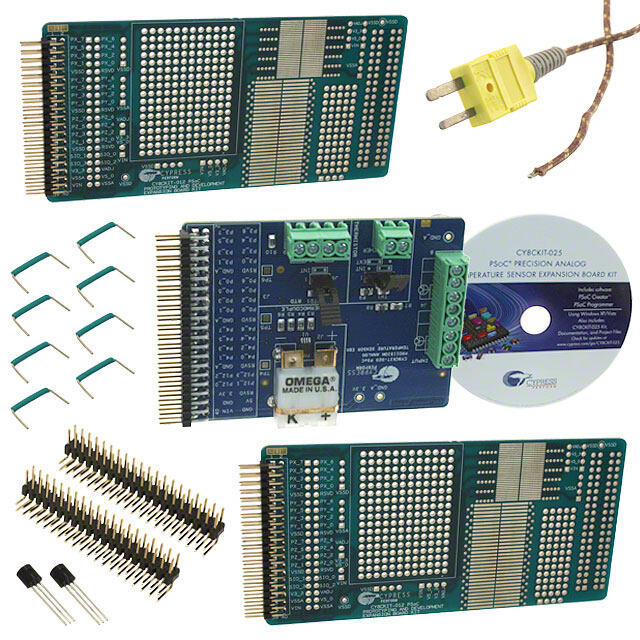
| 描述 | BOARD EVAL ADIS16407加速传感器开发工具 ADIS16407 Eval Brd |
| 产品分类 | |
| 品牌 | Analog Devices |
| 产品手册 | |
| 产品图片 |
|
| rohs | RoHS 合规性豁免无铅 / 符合限制有害物质指令(RoHS)规范要求 |
| 产品系列 | 传感器开发工具,加速传感器开发工具,Analog Devices ADIS16407/PCBZiMEMS®, iSensor™ |
| 数据手册 | 点击此处下载产品Datasheet点击此处下载产品Datasheet点击此处下载产品Datasheet点击此处下载产品Datasheet |
| 产品型号 | ADIS16407/PCBZ |
| PCN过时产品 | |
| 产品种类 | 加速传感器开发工具 |
| 传感器类型 | 加速计,气压,陀螺仪,磁力计,3轴 |
| 传感轴 | Triple |
| 使用的IC/零件 | ADIS16407 |
| 其它名称 | ADIS16407PCBZ |
| 加速 | +/- 18 g |
| 商标 | Analog Devices |
| 封装 | Bulk |
| 嵌入式 | 否 |
| 工作电压 | 4.75 V to 5.25 V |
| 工具用于评估 | ADIS16407 |
| 工厂包装数量 | 1 |
| 感应范围 | ±18g, ±75°/秒, ±150°/秒, ±300°/秒, ±2.5高斯 |
| 所含物品 | 板 |
| 接口 | SPI 串行 |
| 接口类型 | SPI |
| 最大工作温度 | + 105 C |
| 最小工作温度 | - 40 C |
| 标准包装 | 1 |
| 灵敏度 | 3.33mg/LSB, 0.0125 ~ 0.05°/秒/LSB, 0.5mgauss/LSB |
| 电压-电源 | 4.75 V ~ 5.25 V |
| 系列 | ADIS16407 |
| 软件下载 | http://www.analog.com/static/imported-files/eval_boards/ADIS16407_EvalSoftware.zip |


- 商务部:美国ITC正式对集成电路等产品启动337调查
- 曝三星4nm工艺存在良率问题 高通将骁龙8 Gen1或转产台积电
- 太阳诱电将投资9.5亿元在常州建新厂生产MLCC 预计2023年完工
- 英特尔发布欧洲新工厂建设计划 深化IDM 2.0 战略
- 台积电先进制程称霸业界 有大客户加持明年业绩稳了
- 达到5530亿美元!SIA预计今年全球半导体销售额将创下新高
- 英特尔拟将自动驾驶子公司Mobileye上市 估值或超500亿美元
- 三星加码芯片和SET,合并消费电子和移动部门,撤换高东真等 CEO
- 三星电子宣布重大人事变动 还合并消费电子和移动部门
- 海关总署:前11个月进口集成电路产品价值2.52万亿元 增长14.8%

PDF Datasheet 数据手册内容提取
Ten Degrees of Freedom Inertial Sensor Data Sheet ADIS16407 FEATURES GENERAL DESCRIPTION Triaxial digital gyroscope with digital range scaling The ADIS16407 iSensor® device is a complete inertial system ±75°/sec, ±150°/sec, ±300°/sec settings that includes a triaxial gyroscope, a triaxial accelerometer, a Axis-to-axis alignment, <0.05° triaxial magnetometer, and pressure sensors. Each sensor in Triaxial digital accelerometer, ±18 g minimum the ADIS16407 combines industry-leading iMEMS® technology Triaxial digital magnetometer, ±2.5 gauss minimum with signal conditioning that optimEizes dynamic performance. Digital barometer, 10 mbar to 1200 mbar The factory calibration characterizes each sensor for sensitivity, Calibrated pressure range: 300 mbar to 1100 mbar bias, alignment, and linear acceleration (gyro bias). As a result, Autonomous operation and data collection each sensor has its own dynamic compensation formulas that T No external configuration commands required provide accurate sensor measurements. 210 ms start-up time, 4 ms sleep mode recovery time The ADIS16407 provides a simple, cost-effective method for Factory calibrated sensitivity, bias, and axial alignment integrating acEcurate, multiaxis inertial sensing into industrial Calibration temperature range: −40°C to +85°C systems, especially when compared with the complexity and SPI-compatible serial interface investment associated with discrete designs. All necessary motion Embedded temperature sensor testing and calibration are part of the production process at the Programmable operation and control facLtory, greatly reducing system integration time. Tight orthogonal Automatic and manual bias correction controls alignment simplifies inertial frame alignment in navigation systems. Bartlett window FIR length, number of taps The SPI and register structure provide a simple interface for Digital I/O: data ready, alarm indicator, general-purpose O data collection and configuration control. Alarms for condition monitoring Sleep mode for power management The ADIS16407 has a compatible pinout for systems that currently DAC output voltage use ADIS1635x, ADIS1636x, and ADIS1640x IMU products. Enable external sample clock input up to 1.1 kHz The ADIS16407 is packaged in a module that is approximately Single command self test S 23 mm × 23 mm × 23 mm and has a standard connector interface. Single-supply operation: 4.75 V to 5.25 V 2000 g shock survivability Operating temperature range: −40°C to +105°C B APPLICATIONS Platform stabilization and control Navigation O Robotics FUNCTIONAL BLOCK DIAGRAM DIO1DIO2DIO3DIO4 RST VDD SELF TEST I/O ALARMS MANPAOGWEEMRENT GND TRIAXIAL GYRO OUTPUT CS TRIAXIAL DATA ACCEL REGISTERS CALIBRATION SCLK TRIAXIAL CONTROLLLER AND SPI MAGN FILTERS DIN USER PRESSURE CONTROL REGISTERS DOUT CLOCK TEMP VDD ADIS16407 09797-001 Figure 1. Rev. C Information furnished by Analog Devices is believed to be accurate and reliable. However, no responsibility is assumed by Analog Devices for its use, nor for any infringements of patents or other One Technology Way, P.O. Box 9106, Norwood, MA 02062-9106, U.S.A. rights of third parties that may result from its use. Specifications subject to change without notice. No license is granted by implication or otherwise under any patent or patent rights of Analog Devices. Tel: 781.329.4700 www.analog.com Trademarks and registered trademarks are the property of their respective owners. Fax: 781.461.3113 ©2011 Analog Devices, Inc. All rights reserved.
ADIS16407 Data Sheet TABLE OF CONTENTS Features .............................................................................................. 1 Data Ready Indicator ................................................................. 17 Applications ....................................................................................... 1 General-Purpose Input/Output................................................ 17 General Description ......................................................................... 1 Auxiliary DAC ............................................................................ 17 Functional Block Diagram .............................................................. 1 Digital Processing Configuration ................................................. 18 Revision History ............................................................................... 2 Sample Rate ................................................................................. 18 Specifications ..................................................................................... 3 Input Clock Configuration ....................................................... 18 Timing Specifications .................................................................. 6 Digital Filtering......................................E..................................... 18 Absolute Maximum Ratings ............................................................ 7 Dynamic Range .......................................................................... 18 ESD Caution .................................................................................. 7 Calibration ....................................................................................... 19 Pin Configuration and Function Descriptions ............................. 8 Gyroscopes .........................T......................................................... 19 Typical Performance Characteristics ............................................. 9 Accelerometers ........................................................................... 20 Basic Operation ............................................................................... 10 Magnetometer Calibration ........................................................ 20 E Reading Sensor Data .................................................................. 10 Flash Updates .............................................................................. 21 Output Data Registers ................................................................ 11 Restoring Factory Calibration .................................................. 21 Input ADC Channel ................................................................... 13 AlarmsL .............................................................................................. 22 Device Configuration ................................................................ 13 Static Alarm Use ......................................................................... 22 User Registers .................................................................................. 14 Dynamic Alarm Use .................................................................. 22 O System Functions ............................................................................ 15 Alarm Reporting ........................................................................ 22 Global Commands ..................................................................... 15 Applications Information .............................................................. 23 Power Management .................................................................... 15 Installation/Handling................................................................. 23 S Product Identification ................................................................ 15 Gyroscope Bias Optimization ................................................... 23 Memory Management ............................................................... 15 Interface Printed Circuit Board (PCB) .................................... 23 Self Test Function ...........................................B............................ 16 Outline Dimensions ....................................................................... 24 Status/Error Flags ....................................................................... 16 Ordering Guide .......................................................................... 24 Input/Output Configuration ......................................................... 17 O REVISION HISTORY 10/11—Rev. B to Rev. C Added Barometer Section; Changes to Table 40 ........................ 16 Change to Burst Read Function Section and Figure 12 ............ 10 Changes to Table 55, Table 56, Table 57 ...................................... 20 Changed .25 mg to 3.333 mg ........................................ Throughout Changes to Table 58, Table 59, Table 60 ...................................... 21 Changes to System Functions Section ......................................... 15 Change to Product Identification Section ................................... 15 6/11—Rev. 0 to Rev. A Change to Table 36 ......................................................................... 15 Changes to Device Configuration Section and Figure 16 ......... 13 Changes to Digital Filtering Section, Table 47, Caption for Changes to Figure 19 ...................................................................... 18 Figure 18, and Figure 19 ................................................................ 18 Changes to Figure 25 Caption ...................................................... 24 Change to Table 67 ......................................................................... 22 Changes to Ordering Guide .......................................................... 24 7/11—Rev. A to Rev. B 4/11—Revision 0: Initial Version Change to Table 1, Barometer, Sensitivity Parameter .................. 4 Rev. C | Page 2 of 24
Data Sheet ADIS16407 SPECIFICATIONS T = 25°C, VDD = 5 V, angular rate = 0°/sec, dynamic range = ±300°/sec ± 1 g, unless otherwise noted. A Table 1. Parameter Test Conditions/Comments Min Typ Max Unit GYROSCOPES Dynamic Range ±300 ±350 °/sec Initial Sensitivity Dynamic range = ±300°/sec 0.0495 0.05 0.0505 °/sec/LSB Dynamic range = ±150°/sec 0.025 °/sec/LSB Dynamic range = ±75°/sec 0.0125 °/sec/LSB E Sensitivity Temperature Coefficient −40°C ≤ T ≤ +85°C ±40 ppm/°C A Misalignment Axis to axis ±0.05 Degrees Axis to frame (package) ±0.5 Degrees Nonlinearity Best fit straight line T±0.1 % of FS Initial Bias Error ±1 σ ±3 °/sec In-Run Bias Stability 1 σ, SMPL_PRD = 0x0001 0.007 °/sec Angular Random Walk 1 σ, SMPL_PRD = 0x0001 E 1.9 °/√hr Bias Temperature Coefficient −40°C ≤ T ≤ +85°C ±0.01 °/sec/°C A Linear Acceleration Effect on Bias Any axis, 1 σ (MSC_CTRL[7] = 1) 0.05 °/sec/g Bias Voltage Sensitivity VDD = 4.75 V to 5.25 V ±0.3 °/sec/V L Output Noise ±300°/sec range, no filtering 0.8 °/sec rms Rate Noise Density f = 25 Hz, ±300°/sec range, no filtering 0.044 °/sec/√Hz rms 3 dB Bandwidth 330 Hz Sensor Resonant Frequency O 14.5 kHz ACCELEROMETERS Each axis Dynamic Range ±18 g Initial Sensitivity 3.285 3.33 3.38 mg/LSB Sensitivity Temperature Coefficient −40°C S≤ T ≤ +85°C ±50 ppm/°C A Misalignment Axis to axis 0.2 Degrees Axis to frame (package) ±0.5 Degrees Nonlinearity Best fit straight line 0.1 % of FS B Initial Bias Error ±1 σ ±50 mg In-Run Bias Stability 1 σ, SMPL_PRD = 0x0001 0.2 mg Velocity Random Walk 1 σ, SMPL_PRD = 0x0001 0.2 m/sec/√hr Bias Temperature CoefficieOnt −40°C ≤ TA ≤ +85°C ±0.3 mg/°C Bias Voltage Sensitivity VDD = 4.75 V to 5.25 V 2.5 mg/V Output Noise No filtering 9 mg rms Noise Density No filtering 0.5 mg/√Hz rms 3 dB Bandwidth 330 Hz Sensor Resonant Frequency 5.5 kHz MAGNETOMETER Dynamic Range ±2.5 ±3.5 gauss Initial Sensitivity 25°C 0.49 0.5 0.51 mgauss/LSB Sensitivity Temperature Coefficient 25°C, 1 σ 600 ppm/°C Misalignment Axis to axis 0.25 Degrees Axis to frame (package) 0.5 Degrees Nonlinearity Best fit straight line 0.5 % of FS Initial Bias Error 25°C, 0 gauss stimulus ±4 mgauss Bias Temperature Coefficient −40°C ≤ T ≤ +85°C 0.5 mgauss/°C A Output Noise 25°C, no filtering, rms 1.15 mgauss Noise Density 25°C, no filtering, rms 0.06 mgauss/√Hz Bandwidth −3 dB 1540 Hz Rev. C | Page 3 of 24
ADIS16407 Data Sheet Parameter Test Conditions/Comments Min Typ Max Unit BAROMETER Pressure Range Operating 300 1100 mbar Extended1 10 1200 mbar Sensitivity 0.3125 µbar/LSB Total Error 25°C, 300 mbar to 1100 mbar 1.5 mbar Relative Error2 −40°C to +85°C, 300 mbar to 1100 mbar 2.5 mbar Linearity3 25°C, 300 mbar to 1100 mbar 0.1 % of FS −40°C to +85°C, 300 mbar to 1100 mbar 0.15 % of FS E Noise 0.027 mbar rms TEMPERATURE SENSOR Scale Factor 25°C, output = 0x0000 0.14 °C/LSB ADC INPUT T Resolution 12 Bits Integral Nonlinearity ±2 LSB Differential Nonlinearity ±1 LSB E Offset Error ±4 LSB Gain Error ±2 LSB Input Range 0 3.3 V Input Capacitance During acquisition L 20 pF DAC OUTPUT 5 kΩ/100 pF to GND Resolution 12 Bits Relative Accuracy 101 LSB ≤ input code ≤ 4O095 LSB ±4 LSB Differential Nonlinearity ±1 LSB Offset Error ±5 mV Gain Error ±0.5 % Output Range 0 3.3 V S Output Impedance 2 Ω Output Settling Time 10 µs LOGIC INPUTS4 Input High Voltage, V B 2.0 V IH Input Low Voltage, V 0.8 V IL CS signal to wake up from sleep mode 0.55 V CS Wake-Up Pulse Width 20 μs O Logic 1 Input Current, I V = 3.3 V ±0.2 ±10 µA IH IH Logic 0 Input Current, I V = 0 V IL IL All Pins Except RST 40 60 µA RST Pin 1 mA Input Capacitance, C 10 pF IN DIGITAL OUTPUTS4 Output High Voltage, V I = 1.6 mA 2.4 V OH SOURCE Output Low Voltage, V I = 1.6 mA 0.4 V OL SINK FLASH MEMORY Endurance5 10,000 Cycles Data Retention6 T = 85°C 20 Years J FUNCTIONAL TIMES7 Time until new data is available Power-On Start-Up Time 220 ms Reset Recovery Time 105 ms Sleep Mode Recovery Time 7 ms Flash Memory Update Time 75 ms Flash Memory Test Time 30 ms Automatic Self Test Time SMPL_PRD = 0x0001 52 ms Rev. C | Page 4 of 24
Data Sheet ADIS16407 Parameter Test Conditions/Comments Min Typ Max Unit CONVERSION RATE SPS xGYRO_OUT, xACCL_OUT, xMAGN_OUT SMPL_PRD = 0x0001 819.2 SPS BAR_OUT, BARO_OUTL8 SMPL_PRD = 0x0001 51.2 SPS Clock Accuracy ±3 % Sync Input Clock9 0.8 1.1 kHz POWER SUPPLY Operating voltage range, VDD 4.75 5.0 5.25 V Power Supply Current 70 mA Sleep mode 1.4 mA 1 The extended pressure range is guaranteed by design. E 2 The relative error assumes that the initial error, at +25°C, is corrected in the end application. 3 Linearity errors assume a full scale (FS) of 1000 mbar. 4 The digital I/O signals are driven by an internal 3.3 V supply, and the inputs are 5 V tolerant. 5 Endurance is qualified as per JEDEC Standard 22, Method A117, and measured at −40°C, +25°C, +85°C, and +125°C. 6 The data retention lifetime equivalent is at a junction temperature (TJ) of 85°C as per JEDEC Standard 22, Method A117T. Data retention lifetime decreases with junction temperature. 7 These times do not include thermal settling and internal filter response times (330 Hz bandwidth), which may affect overall accuracy. 8 The BARO_OUT and BARO_OUTL registers sample at a rate that is 1/16th that of the other output registers. 9 The sync input clock functions below the specified minimum value, but at reduced performance levels. E L O S B O Rev. C | Page 5 of 24
ADIS16407 Data Sheet TIMING SPECIFICATIONS T = 25°C, VDD = 5 V, unless otherwise noted. A Table 2. Normal Mode Burst Read Parameter Description Min1 Typ Max Min1 Typ Max Unit f Serial clock 0.01 2.0 0.01 1.0 MHz SCLK t Stall period between data 9 1/f µs STALL SCLK t Read rate 40 µs READRATE t Chip select to SCLK edge 48.8 48.8 ns CS E t DOUT valid after SCLK edge 100 100 ns DAV t DIN setup time before SCLK rising edge 24.4 24.4 ns DSU t DIN hold time after SCLK rising edge 48.8 48.8 ns DHD tSCLKR, tSCLKF SCLK rise/fall times, not shown in Timing Diagrams 5 12.5 T 5 12.5 ns t , t DOUT rise/fall times, not shown in Timing Diagrams 5 12.5 5 12.5 ns DR DF t CS high after SCLK edge 5 5 ns SFS t Input sync positive pulse width 5 5 µs 1 E t Input sync low time 100 100 µs x t Input sync to data ready output 600 600 µs 2 t Input sync period 910 910 µs 3 L 1 Guaranteed by design and characterization, but not tested in production. Timing Diagrams O CS tCS tSFS 1 2 3 S4 5 6 15 16 SCLK tDAV DOUT MSB DB14 DB13 DB12 DB11 DB10 DB2 DB1 LSB B tDSU tDHD DIN R/W A6 A5 A4 A3 A2 D2 D1 LSB 09797-002 O Figure 2. SPI Timing and Sequence tREADRATE tSTALL CS SCLK 09797-003 Figure 3. Stall Time and Data Rate t3 t2 t1 tX SYNC CLOCK (DIO4) REDAADTAY 07570-004 Figure 4. Input Clock Timing Diagram Rev. C | Page 6 of 24
Data Sheet ADIS16407 ABSOLUTE MAXIMUM RATINGS Table 3. Stresses above those listed under Absolute Maximum Ratings Parameter Rating may cause permanent damage to the device. This is a stress Acceleration rating only; functional operation of the device at these or any Any Axis, Unpowered 2000 g other conditions above those indicated in the operational Any Axis, Powered 2000 g section of this specification is not implied. Exposure to absolute VDD to GND −0.3 V to +6.0 V maximum rating conditions for extended periods may affect Digital Input Voltage to GND −0.3 V to +5.3 V device reliability. Digital Output Voltage to GND −0.3 V to +3.6 V Table 4. Package Characteristics E Analog Input to GND −0.3 V to +3.6 V Package Type θ θ Device Weight Temperature JA JC 24-Lead Module 39.8°C/W 14.2°C/W 16 grams Operating Range −40°C to +105°C (ML-24-2) Storage Range −65°C to +125°C1, 2 T Pressure 6 bar 1 Extended exposure to temperatures outside the specified temperature ESD CAUTION range of −40°C to +105°C can adversely affect the accuracy of the factory E calibration. For best accuracy, store the parts within the specified operating range of −40°C to +105°C. 2 Although the device is capable of withstanding short-term exposure to 150°C, long-term exposure threatens internal mechanical integrity. L O S B O Rev. C | Page 7 of 24
ADIS16407 Data Sheet PIN CONFIGURATION AND FUNCTION DESCRIPTIONS ADIS16407 TOP VIEW (Not to Scale) DC A DIO3 SCLK DIN DIO1 DIO2 VDD GND GND DNC DNC AUX_ DNC 1 3 5 7 9 11 13 15 17 19 21 23 2 4 6 8 10 12 14 16 18 20 22 24 N T S T D D D C C C C C DIO4/CLKI DOU C RS VD VD GN DN DN AUX_DA DN DN PIN 23 E N1234....O TDWMTHNAHEICTSSE I N=NV GIDCE OOWC NON RNNOEENTPCE CRTCOEETSDNOE,N RNTE:HT CSSETA .TPMHINTEES TC AO CRPLE MV NI-EO1W1T2 -VO0I2FS IOTBHRLE EE .MQAUTIVINAGLE CNOTN.NECTOR. 09797-005 PIN 1 T 09797-006 Figure 5. Pin Configuration Figure 6. Axial Orientation E Table 5. Pin Function Descriptions Pin No. Mnemonic Type1 Description 1 DIO3 I/O ConfiLgurable Digital Input/Output. 2 DIO4/CLKIN I/O Configurable Digital Input/Output or Sync Clock Input. 3 SCLK I SPI Serial Clock. 4 DOUT O SPI Data Output. Clocks the output on the SCLK falling edge. O 5 DIN I SPI Data Input. Clocks the input on the SCLK rising edge. 6 CS I SPI Chip Select. 7 DIO1 I/O Configurable Digital Input/Output. 8 RST I Reset. S 9 DIO2 I/O Configurable Digital Input/Output. 10, 11, 12 VDD S Power Supply. 13, 14, 15 GND S Power Ground. 16, 17, 18, 19, 22, 23, 24 DNC B N/A Do Not Connect. Do not connect to these pins. 20 AUX_DAC O Auxiliary, 12-Bit DAC Output. 21 AUX_ADC I Auxiliary, 12-Bit ADC Input. 1 S is supply, O is output, I is input, N/A isO not applicable. Rev. C | Page 8 of 24
Data Sheet ADIS16407 TYPICAL PERFORMANCE CHARACTERISTICS 0.1 0.01 c) E(°/se CE(g) C N AN +1σ RIA RI A VA 0.01 NV 0.001 N MEAN A A L OTALL –1σ OOTAL E +1σ RO R MEAN –1σ T 0.0010.1 1 10Tau (sec)100 1k 10k 09797-007 0.00010.1 1 10Tau (sec)100 1k 10k 09797-008 Figure 7. Gyroscope Root Allan Variance Figure 8. Accelerometer Root Allan Variance E L O S B O Rev. C | Page 9 of 24
ADIS16407 Data Sheet BASIC OPERATION The ADIS16407 is an autonomous system that requires no user READING SENSOR DATA initialization. When it has a valid power supply, it initializes itself The ADIS16407 provides two different options for acquiring and starts sampling, processing, and loading sensor data into sensor data: single register and burst register. A single register the output registers at a sample rate of 819.2 SPS. DIO1 pulses read requires two 16-bit SPI cycles. The first cycle requests the high after each sample cycle concludes. The SPI interface enables contents of a register using the bit assignments in Figure 13. simple integration with many embedded processor platforms, Bit DC7 to Bit DC0 are don’t care for a read, and then the output as shown in Figure 9 (electrical connection) and Table 6 (pin register contents follow on DOUT during the second sequence. functions). Figure 10 includes three single register reads in succession. In VDD I/O L3I.N3VE SO ARR 5EV CLOOMGPICA LTEIBVLEEL WSITH 5V this example, the process starts with DINE = 0x0400 to request the contents of XGYRO_OUT, then follows with 0x0600 to 10 11 12 SPYRSOTCEEMSSOR SS 6 CS ADIS16407 request YGYRO_OUT and 0x0800 to request ZGYRO_OUT. SPI MASTER SCLK 3 SCLK Full duplex operation enableTs processors to use the same 16-bit MOSI 5 DIN SPI cycle to read data from DOUT while requesting the next set MISO 4 DOUT of data on DIN. Figure 11 provides an example of the four SPI IRQ 7 DIO1 signals when readiEng XGYRO_OUT in a repeating pattern. 13 14 15 Figure 9. Electrical Connection Diagram 09797-009 DODUINT 0x0400 XG0YxR0O6_0O0UT YG0YxR0O8_0O0UT ZGYRO_OUT 09797-010 L Figure 10. SPI Read Example Table 6. Generic Master Processor Pin Names and Functions Pin Name Function CS SS Slave select SCLK O SCLK Serial clock DIN DIN = 0000 0100 0000 0000 = 0x0400 MOSI Master output, slave input MISO Master input, slave output DOUTDOUT = 1111 1001 1101 1010 = 0xF9DA = –1574 LSBs => –19.675°/sec 09797-011 IRQ Interrupt request S Figure 11. Example SPI Read, Second 16-Bit Sequence The ADIS16407 SPI interface supports full duplex serial commu- Burst Read Function nication (simultaneous transmit and receive) and uses the bit The burst read function enables the user to read all output registers sequence shown in Figure 13. Table 7 provides a list of the most B using one command on the DIN line and shortens the stall time common settings that require attention to initialize the serial between each 16-bit segment to one SCLK cycle (see Table 2). port of a processor for the ADIS16407 SPI interface. Figure 12 provides the burst read sequence of data on each SPI Table 7. Generic Master Processor SPI Settings signal. The sequence starts with writing 0x4200 to DIN, followed Processor Setting DescriptioOn by each output register clocking out on DOUT, in the order in Master The ADIS16407 operates as a slave which they appear in Table 8. SCLK Rate ≤ 2 MHz1 Maximum serial clock rate CS 1 2 3 15 SPI Mode 3 CPOL = 1 (polarity), CPHA = 1 (phase) MSB-First Mode Bit sequence SCLK 16-Bit Mode Shift register/data length DIN 0x4200 DON’T CARE 1 For burst read, SCLK rate ≤ 1 MHz. DOUT SUPPLY_OUT XGYRO_OUT AUX_ADC 09797-012 Figure 12. Burst Read Sequence CS SCLK DIN R/W A6 A5 A4 A3 A2 A1 A0 DC7 DC6 DC5 DC4 DC3 DC2 DC1 DC0 R/W A6 A5 DOUT D15 D14 D13 D12 D11 D10 D9 D8 D7 D6 D5 D4 D3 D2 D1 D0 D15 D14 D13 NOTES 1 2 .. TIIFNH RET/H WDEO =PU R1T E DBVUIITRO IPUNASGT 1TT6EH-BREIN TP RRDEEINFV LISOEEUCQSTU SSE ETNQHCEUE E EWNNHCTEEIRN, ED R OC/WUOT N= TI S0E. NNTOST ODFE FTIHNEE DR.EGISTER IDENTIFIED BY [A6:A0] 09797-013 Figure 13. SPI Communication Bit Sequence Rev. C | Page 10 of 24
Data Sheet ADIS16407 OUTPUT DATA REGISTERS [14] Error/alarm, 1 = active, see DIAG_STAT for error flags [13:0] Y-axis gyroscope data, twos complement format, The output registers in Table 8 provide the most recent sensor 0.05°/sec per LSB, when SENS_AVG[15:8] = 0x04 data produced by the ADIS16407. Each output register has flags for new data indication and error/alarm conditions, which Table 11. ZGYRO_OUT (Base Address = 0x08), Read Only reduces the need to monitor DIAG_STAT. Bits Description [15] New data indicator (ND), 1 = new data in register Table 8. Output Data Register Formats [14] Error/alarm, 1 = active, see DIAG_STAT for error flags Register Address Measurement [13:0] Z-axis gyroscope data, twos complement format, SUPPLY_OUT 0x02 Power supply 0.05°/sec per LSB, when SENS_AVG[15:8] = 0x04 XGYRO_OUT 0x04 Gyroscope, x-axis E YGYRO_OUT 0x06 Gyroscope, y-axis Table 12. Rotation Rate, Twos Complement Format ZGYRO_OUT 0x08 Gyroscope, z-axis Rotation Rate Decimal Hex Binary XACCL_OUT 0x0A Accelerometer, x-axis +300°/sec +6000 0x1770 xx01 0111 0111 0000 YACCL_OUT 0x0C Accelerometer, y-axis +0.1°/sec +2 T 0x0002 xx00 0000 0000 0010 ZACCL_OUT 0x0E Accelerometer, z-axis +0.05°/sec +1 0x0001 xx00 0000 0000 0001 XMAGN_OUT 0x10 Magnetometer, x-axis 0°/sec 0 0x0000 xx00 0000 0000 0000 YMAGN_OUT 0x12 Magnetometer, y-axis −0.05°/sec E−1 0x3FFF xx11 1111 1111 1111 ZMAGN_OUT 0x14 Magnetometer, z-axis −0.1°/sec −2 0x3FFE xx11 1111 1111 1110 BARO_OUT 0x16 Barometer/pressure, higher −300°/sec −6000 0x2890 xx10 1000 1001 0000 BARO_OUTL 0x18 Barometer/pressure, lower Accelerometers TEMP_OUT1 0x1A Internal temperature L AUX_ADC 0x1C Auxiliary ADC Figure 14 provides arrows (aX, aY, aZ) that indicate the direction of acceleration, which produces a positive response in the 1 This is most useful for monitoring relative changes in the temperature. gyroscope output registers: XACCL_OUT (x-axis, Table 13), O Z-AXIS YACCL_OUT (y-axis, Table 14), and ZACCL_OUT (z-axis, aZ mZ Table 15). Table 16 illustrates the accelerometer data format. gZ Table 13. XACCL_OUT (Base Address = 0x0A), Read Only S Bits Description [15] New data indicator (ND), 1 = new data in register Y-AXIS aY mX X-AXIS [14] Error/alarm, 1 = active, see DIAG_STAT for error flags mY B aX [13:0] X-axis acceleration data, twos complement format, 3.333 mg per LSB gY gX Table 14. YACCL_OUT (Base Address = 0x0C), Read Only O 09797-014 B[1i5ts] NDeewsc driapttai oinnd icator (ND), 1 = new data in register Figure 14. Inertial Sensor Direction Reference [14] Error/alarm, 1 = active, see DIAG_STAT for error flags Gyroscopes [13:0] Y-axis acceleration data, twos complement format, 3.333 mg per LSB Figure 14 provides arrows (g , g , g ) that indicate the direction X Y Z of rotation, which produces a positive response in the gyroscope Table 15. ZACCL_OUT (Base Address = 0x0E), Read Only output registers: XGYRO_OUT (x-axis, Table 9), YGYRO_OUT Bits Description (y-axis, Table 10), and ZGYRO_OUT (z-axis, Table 11). Table 12 [15] New data indicator (ND), 1 = new data in register illustrates the gyroscope data format. [14] Error/alarm, 1 = active, see DIAG_STAT for error flags Table 9. XGYRO_OUT (Base Address = 0x04), Read Only [13:0] Z-axis acceleration data, twos complement format, Bits Description 3.333 mg per LSB [15] New data indicator (ND), 1 = new data in register [14] Error/alarm, 1 = active, see DIAG_STAT for error flags [13:0] X-axis gyroscope data, twos complement format, 0.05°/sec per LSB, when SENS_AVG[15:8] = 0x04 Table 10. YGYRO_OUT (Base Address = 0x06), Read Only Bits Description [15] New data indicator (ND), 1 = new data in register Rev. C | Page 11 of 24
ADIS16407 Data Sheet Table 16. Acceleration, Twos Complement Format Use BAR_OUTL and the following steps to increase the Acceleration Decimal Hex Binary numerical resolution by 8-bits for best performance: +18 g +5401 0x1519 xx01 0101 0001 1001 1. Read BAR_OUT and multiply by 256 (shift 8 bits) +6.667 mg +2 0x0002 xx00 0000 0000 0010 2. Read BAR_OUTL and max off upper 8 bits +3.333 mg +1 0x0001 xx00 0000 0000 0001 3. Add results together for a 24-bit result, 0 g 0 0x0000 xx00 0000 0000 0000 where 1 LSB = 0.0003125 and 0x00000 = 0 mbar −3.333 mg −1 0x3FFF xx11 1111 1111 1111 −6.667 mg −2 0x3FFE xx11 1111 1111 1110 Table 21. BARO_OUT (Base Address = 0x16), Read Only −18 g −5401 0x2AE7 xx10 1010 1110 0111 Bits Description [15] New data indicator (ND), 1 = new data in register Magnetometers E [14] Error/alarm, 1 = active, see DIAG_STAT for error flags Figure 14 provides arrows (mX, mY, mZ) that indicate the direction [13:0] Barometric pressure data, binary data format, of the magnetic field, which produces a positive response in the 0.08 mbar per LSB, 0x0000 = 0 mbar gyroscope output registers: XMAGN_OUT (x-axis, Table 17), T YMAGN_OUT (y-axis, Table 18), and ZAMAGN_OUT (z-axis, Table 22. BARO_OUTL (Base Address = 0x18), Read Only Table 19). Table 20 illustrates the magnetic field intensity data Bits Description format. [15:8] Not used E [7:0] Barometric pressure data, binary data format, Table 17. XMAGN_OUT (Base Address = 0x10), Read Only 0.0003125 mbar per LSB, 0x0000 = 0 mbar Bits Description [15] New data indicator (ND), 1 = new data in register Table 23. Pressure, Binary, BARO_OUT Only L Pressure [14] Error/alarm, 1 = active, see DIAG_STAT for error flags (mbar) Decimal Hex Binary [13:0] X-axis magnetic field intensity data, twos complement 1200 15,000 0x3A98 xx11 1010 1001 1000 format, 0.5 mgauss per LSB O1100 13,750 0x35B6 xx11 0101 1011 0110 Table 18. YMAGN_OUT (Base Address = 0x12), Read Only 1000 12,500 0x30D4 xx11 0000 1101 0100 Bits Description 0.16 2 0x0002 xx00 0000 0000 0010 [15] New data indicator (ND), 1 = new data in register 0.08 1 0x0001 xx00 0000 0000 0001 [14] Error/alarm, 1 = active, see DIAG_STAT for error Sflags 0 0 0x0000 xx00 0000 0000 0000 [13:0] Y-axis magnetic field intensity data, twos complement Internal Temperature format, 0.5 mgauss per LSB The internal temperature measurement data loads into the Table 19. ZMAGN_OUT (Base Address = 0Bx14), Read Only TEMP_OUT (Table 24) register. Table 25 illustrates the Bits Description temperature data format. [15] New data indicator (ND), 1 = new data in register Table 24. TEMP_OUT (Base Address = 0x1A), Read Only [14] Error/alarm, 1 = active, see DIAG_STAT for error flags O Bits Description [13:0] Z-axis magnetic field intensity data, twos complement format, 0.5 mgauss per LSB [15] New data indicator (ND), 1 = new data in register [14] Error/alarm, 1 = active, see DIAG_STAT for error flags Table 20. Magnetometer, Twos Complement Format [13:12] Not used Magnetic Field Decimal Hex Binary [11:0] Internal temperature data, twos complement, +2.5 gauss +5000 0x1388 xx01 0011 1000 1000 0.136°C/LSB, 25°C = 0x000 +0.001 gauss +2 0x0002 xx00 0000 0000 0010 +0.0005 gauss +1 0x0001 xx00 0000 0000 0001 Table 25. Temperature, Twos Complement Format 0 gauss 0 0x0000 xx00 0000 0000 0000 Temperature Decimal Hex Binary −0.0005 gauss −1 0x3FFF xx11 1111 1111 1111 +105°C +588 LSB 0x24C xxxx 0010 0100 1100 −0.0005 gauss −2 0x3FFE xx11 1111 1111 1110 +85°C +441 LSB 0x1B9 xxxx 0001 1011 1001 −2.5 gauss −5000 0x2C78 xx10 1100 0111 1000 +25.272°C +2 LSB 0x002 xxxx 0000 0000 0010 +25.136°C +1 LSB 0x001 xxxx 0000 0000 0001 Barometric Pressure +25°C 0 LSB 0x000 xxxx 0000 0000 0000 The barometric pressure measurements are contained in two +24.864°C −1 LSB 0xFFF xxxx 1111 1111 1111 registers, BARO_OUT (Table 21) and BARO_OUTL (Table 22) +24.728°C −2 LSB 0xFFE xxxx 1111 1111 1110 registers. Table 23 provides several numerical format examples −40°C −478 LSB 0xE22 xxxx 1110 0010 0010 for BARO_OUT, which is sufficient for most applications. Rev. C | Page 12 of 24
Data Sheet ADIS16407 Power Supply Table 29. Analog Input, Offset Binary Format Input Voltage Decimal Hex Binary The SUPPLY_OUT register (Table 26) provides a measurement of the voltage that is on the VDD pins of the device. Table 27 3.3 V 4095 0xFFF xxxx 1111 1111 1111 illustrates the power supply data format. 1 V 1241 0x4D9 xxxx 0100 1101 1001 1.6118 mV 2 0x002 xxxx 0000 0000 0010 Table 26. SUPPLY_OUT (Base Address = 0x02), Read Only 805.9 µV 1 0x001 xxxx 0000 0000 0001 Bits Description 0 V 0 0x000 xxxx 0000 0000 0000 [15] New data indicator (ND), 1 = new data in register DEVICE CONFIGURATION [14] Error/alarm, 1 = active, see DIAG_STAT for error flags The control registers in Table 30 provide users with a variety of [13:12] Not used configuration options. The SPI providEes access to these registers, [11:0] Power supply measurement data, binary format, 2.418 mV/LSB, 0 V = 0x000 one byte at a time, using the bit assignments in Figure 13. Each register has 16 bits, where Bits[7:0] represent the lower address, Table 27. Power Supply Data, Binary Format and Bits[15:8] represent the upper address. Figure 16 provides T Voltage Decimal Hex Binary an example of writing 0x03 to Address 0x3B (SMPL_PRD[15:8]), +5.25 V 2171 0x87B xxxx 1000 0111 1011 using DIN = 0xBB03. This example reduces the sample rate by a +5.0 V 2068 0x814 xxxx 1000 0001 0100 factor of eight (see Table 46). +4.75 V 1964 0x7AC xxxx 0111 1010 1100 E CS 1 V 414 0x19E xxxx 0001 1001 1110 4.836 mV 2 0x002 xxxx 0000 0000 0010 SCLK 2.418 mV 1 0x001 xxxx 0000 0000 0001 0 V 0 0x000 xxxx 0000 0000 0000 DLIDNI N= 1011 1011 0000 0011 = 0xBB03, WRITES 0x03TOADDRESS 0x3B. 09797-016 INPUT ADC CHANNEL Figure 16. Example SPI Write Sequence The AUX_ADC register provides access to the auxiliary ADC O Dual Memory Structure input channel. The ADC is a 12-bit successive approximation Writing configuration data to a control register updates its SRAM converter that has an input circuit equivalent to the one shown contents, which are volatile. After optimizing each relevant control in Figure 15. The maximum input is 3.3 V. The ESD protection register setting in a system, set GLOB_CMD[3] = 1 (DIN = diodes can handle 10 mA without causing irreversibSle damage. 0xBE08) to backup these settings in nonvolatile flash memory. The on resistance (R1) of the switch has a typical value of 100 Ω. The flash backup process requires a valid power supply level for The sampling capacitor, C2, has a typical value of 16 pF. the entire 75 ms process time. Table 30 provides a user register VCC B memory map that includes a flash backup column. A “yes” in this column indicates that a register has a mirror location in flash and, D R1 C2 when backed up properly, it automatically restores itself during C1 DO 09797-015 smtaermtuopr yo rs tarfutecrt uar ree useste.d F tiog umrea n1a7g pe roopveidraetsi oan d aiangdr asmto roef ctrhieti cdaul aul ser settings. Figure 15. Equivalent Analog Input Circuit (Conversion Phase: Switch Open, Track Phase: Switch Closed) MANUAL FLASH BACKUP Table 28. AUX_ADC (Base Address = 0x1C), Read Only NONVOLATILE VOLATILE Bits Description FLASH MEMORY SRAM [15] New data indicator (ND), 1 = new data in register (NO SPI ACCESS) SPI ACCESS [14] Error/alarm, 1 = active, see DIAG_STAT for error flags START-UP [[1131::102] ] ANnoat luosge idn put channel data, binary format, RESET 09797-017 0.8059 mV/LSB, 0 V = 0x000 Figure 17. SRAM and Flash Memory Diagram Rev. C | Page 13 of 24
ADIS16407 Data Sheet USER REGISTERS Table 30. User Register Memory Map1 Name R/W Flash Backup Address2 Default Function Bit Assignments FLASH_CNT R Yes 0x00 N/A Flash memory write count See Table 38 SUPPLY_OUT R No 0x02 N/A Power supply measurement See Table 26 XGYRO_OUT R No 0x04 N/A X-axis gyroscope output See Table 9 YGYRO_OUT R No 0x06 N/A Y-axis gyroscope output See Table 10 ZGYRO_OUT R No 0x08 N/A Z-axis gyroscope output See Table 11 XACCL_OUT R No 0x0A N/A X-axis accelerometer output See Table 13 E YACCL_OUT R No 0x0C N/A Y-axis accelerometer output See Table 14 ZACCL_OUT R No 0x0E N/A Z-axis accelerometer output See Table 15 XMAGN_OUT R No 0x10 N/A X-axis magnetometer measurement See Table 17 YMAGN_OUT R No 0x12 N/A Y-axis magnetometer measuremTent See Table 18 ZMAGN_OUT R No 0x14 N/A Z-axis magnetometer measurement See Table 19 BARO_OUT R No 0x16 N/A Barometer pressure measurement, high word See Table 21 BARO_OUTL R No 0x18 N/A Barometer pressure measurement, low word See Table 22 E TEMP_OUT R No 0x1A N/A Temperature output See Table 24 AUX_ADC R No 0x1C N/A Auxiliary ADC measurement See Table 28 XGYRO_OFF R/W Yes 0x1E 0x0000 X-axis gyroscope bias offset factor See Table 49 YGYRO_OFF R/W Yes 0x20 0x0000 Y-axis gyrLoscope bias offset factor See Table 50 ZGYRO_OFF R/W Yes 0x22 0x0000 Z-axis gyroscope bias offset factor See Table 51 XACCL_OFF R/W Yes 0x24 0x0000 X-axis acceleration bias offset factor See Table 52 YACCL_OFF R/W Yes 0x26 0x0000 OY-axis acceleration bias offset factor See Table 53 ZACCL_OFF R/W Yes 0x28 0x0000 Z-axis acceleration bias offset factor See Table 54 XMAGN_HIC R/W Yes 0x2A 0x0000 X-axis magnetometer, hard iron factor See Table 55 YMAGN_HIC R/W Yes 0x2C 0x0000 Y-axis magnetometer, hard iron factor See Table 56 ZMAGN_HIC R/W Yes 0x2E 0x0000 Z-axis magnetometer, hard iron factor See Table 57 S XMAGN_SIC R/W Yes 0x30 0x0800 X-axis magnetometer, soft iron factor See Table 58 YMAGN_SIC R/W Yes 0x32 0x0800 Y-axis magnetometer, soft iron factor See Table 59 ZMAGN_SIC R/W Yes 0x34 0x0800 Z-axis magnetometer, soft iron factor See Table 60 GPIO_CTRL R/W No 0x36B 0x0000 Auxiliary digital input/output control See Table 42 MSC_CTRL R/W Yes 0x38 0x0006 Miscellaneous control See Table 39 SMPL_PRD R/W Yes 0x3A 0x0001 Internal sample period (rate) control See Table 46 SENS_AVG R/W Yes 0x3C 0x0402 Dynamic range and digital filter control See Table 47 O SLP_CTRL W No 0x3E N/A Sleep mode control See Table 33 DIAG_STAT R No 0x40 0x0000 System status See Table 40 GLOB_CMD W N/A 0x42 0x0000 System command See Table 32 ALM_MAG1 R/W Yes 0x44 0x0000 Alarm 1 amplitude threshold See Table 62 ALM_MAG2 R/W Yes 0x46 0x0000 Alarm 2 amplitude threshold See Table 63 ALM_SMPL1 R/W Yes 0x48 0x0000 Alarm 1 sample size See Table 64 ALM_SMPL2 R/W Yes 0x4A 0x0000 Alarm 2 sample size See Table 65 ALM_CTRL R/W Yes 0x4C 0x0000 Alarm control See Table 66 AUX_DAC R/W No 0x4E 0x0000 Auxiliary DAC data See Table 43 Reserved N/A N/A 0x50 N/A Reserved LOT_ID1 R Yes 0x52 N/A Lot identification number See Table 34 LOT_ID2 R Yes 0x54 N/A Lot identification number See Table 35 PROD_ID R Yes 0x56 0x4107 Product identifier See Table 36 SERIAL_NUM R Yes 0x58 N/A Serial number See Table 37 1 N/A means not applicable. 2 Each register contains two bytes. The address of the lower byte is displayed. The address of the upper byte is equal to the address of the lower byte plus 1. Rev. C | Page 14 of 24
Data Sheet ADIS16407 SYSTEM FUNCTIONS The ADIS16407 provides a number of system controls for PRODUCT IDENTIFICATION managing operation, using the registers in Table 31. The PROD_ID register in Table 36 contains the binary equivalent Table 31. System Tool Registers of the part number. It provides a product specific variable for Register Name Address Description systems that need to track this in their system software. The MSC_CTRL 0x38 Self test, calibration, data ready LOT_ID1 and LOT_ID2 registers in Table 34 and Table 35 SLP_CTRL 0x3E Sleep mode control combine to provide a unique, 32-bit lot identification code. The DIAG_STAT 0x40 Error flags SERIAL_NUM register in Table 37 contains a binary number GLOB_CMD 0x42 Single command functions that represents the serial number on the device label. The E LOT_ID1 0x52 Lot Identification Code 1 assigned serial numbers in SERIAL_NUM are lot specific. LOT_ID2 0x54 Lot Identification Code 2 PROD_ID 0x56 Product identifier Table 34. LOT_ID1 (Base Address = 0x52), Read Only SERIAL_NUM 0x58 Serial number Bits Description T [15:0] Lot identification, binary code GLOBAL COMMANDS Table 35. LOT_ID2 (Base Address = 0x54), Read Only The GLOB_CMD register in Table 32 provides trigger bits for E Bits Description software reset, flash memory management, DAC control, and calibration control. Start each of these functions by writing a 1 to [15:0] Lot identification, binary code the assigned bit in GLOB_CMD. After completing the task, the bit Table 36. PROD_ID Bit (Base Address = 0x56), Read Only automatically returns to 0. For example, set GLOB_CMD[7] = 1 L Bits Description (Default = 0x4017) (DIN = 0xC280) to initiate a software reset, which stops the sensor [15:0] Binary number, equivalent to part number operation and runs the device through its start-up sequence. Set Contents = 16,407 = 0x4017 GLOB_CMD[3] = 1 (DIN = 0xC208) to back up the user register O contents in nonvolatile flash. This sequence includes loading Table 37. SERIAL_NUM (Base Address = 0x58), Read Only the control registers with the data in their respective flash Bits Description memory locations prior to producing new data. [15:12] Reserved Table 32. GLOB_CMD (Base Address = 0x42), WrSite Only [11:0] Serial number, 1 to 4094 (0xFFE) Bits Description (Default = 0x0000) [15:8] Not used MEMORY MANAGEMENT [7] Software reset The FLASH_CNT register in Table 38 provides a 16-bit counter B [6:4] Not used that helps track the number of write cycles to the nonvolatile flash [3] Flash update memory. The flash updates every time a manual flash update [2] Auxiliary DAC data latch occurs. A manual flash update is initiated by the GLOB_CMD[3] [1] Factory calibratOion restore bit and is also performed at the completion of the GLOB_CMD[1:0] [0] Gyroscope bias correction functions (see Table 32). POWER MANAGEMENT Table 38. FLASH_CNT (Base Address = 0x00), Read Only The SLP_CTRL register (see Table 33) provides two sleep Bits Description modes for system level management: normal and timed. Set [15:0] Binary counter SLP_CTRL[8] = 1 (DIN = 0xBF01) to start normal sleep mode. Checksum Test When the device is in sleep mode, the following events can cause Set MSC_CTRL[11] = 1 (DIN = 0xB908) to perform a check- it to wake up: asserting CS from high to low, asserting RST from sum test of the internal program memory. This function takes a high to low, or cycling the power. Use SLP_CTRL[7:0] to put the summation of the internal program memory and compares it with device into sleep mode for a specified period. For example, the original summation value for the same locations (from factory SLP_CNT[7:0] = 0x64 (DIN = 0xBE64) puts the ADIS16407 to configuration). Check the results in the DIAG_STAT register, which sleep for 50 seconds. is in Table 40. DIAG_STAT[6] equals 0 if the sum matches the Table 33. SLP_CTRL (Base Address = 0x3E), Write Only correct value, and 1 if it does not. Make sure that the power Bits Description supply is within specification for the entire 20 ms that this [15:9] Not used function takes to complete. [8] Normal sleep mode (1 = start sleep mode) [7:0] Timed sleep mode (write 0x01 to 0xFF to start) Sleep mode duration, binary, 0.5 sec/LSB Rev. C | Page 15 of 24
ADIS16407 Data Sheet SELF TEST FUNCTION STATUS/ERROR FLAGS Gyroscopes/Accelerometers The DIAG_STAT register in Table 40 provides error flags for The MSC_CTRL register in Table 39 provides a self test function a number of functions. Each flag uses 1 to indicate an error con- for the gyroscopes and accelerometers. This function allows the dition and 0 to indicate a normal condition. Reading this register user to verify the mechanical integrity of each MEMS sensor. provides access to the status of each flag and resets all of the bits When enabled, the self test applies an electrostatic force to each to 0 for monitoring future operation. If the error condition remains, internal sensor element, which causes them to move. The move- the error flag returns to 1 at the conclusion of the next sample ment in each element simulates its response to actual rotation/ cycle. DIAG_STAT[0] does not require a read of this register to acceleration and generates a predictable electrical response in the return to 0. If the power supply voltage goes back into range, this sensor outputs. The ADIS16407 exercises this function and flag clears automatically. The SPI communEication error flag in compares the response to an expected range of responses and reports DIAG_STAT[3] indicates that the number of SCLKs in a SPI a pass/fail response to DIAG_STAT[5]. If this is high, the sequence did not equal a multiple of 16 SCLKs. DIAG_STAT[15:10] provide pass/fail flags for each inertial sensor. Table 40. DIAG_STAT (BasTe Address = 0x40), Read Only Table 39. MSC_CTRL (Base Address = 0x38), Read/Write Bits Description (Default = 0x0000) Bits Description (Default = 0x0006) [15] Z-axis accelerometer self test result [15:12] Not used 1 = fail, 0 = pass E [11] Checksum memory test (cleared upon completion)1 [14] Y-axis accelerometer self test result 1 = enabled, 0 = disabled 1 = fail, 0 = pass [10] Internal self test (cleared upon completion)1 [13] X-axis accelerometer self test result 1 = enabled, 0 = disabled L1 = fail, 0 = pass [9:8] Do not use, always set to 00 [12] Z-axis gyroscope self test result [7] Linear acceleration bias compensation for gyroscopes 0 = pass 1 = enabled, 0 = disabled O[11] Y-axis gyroscope self test result [6] Point of percussion, see Figure 6 1 = fail, 0 = pass 1 = enabled, 0 = disabled [10] X-axis gyroscope self test result [5:3] Not used 1 = fail, 0 = pass [2] Data ready enable S [9] Alarm 2 status 1 = enabled, 0 = disabled 1 = active, 0 = inactive [1] Data ready polarity [8] Alarm 1 status 1 = active high, 0 = active low 1 = active, 0 = inactive B [0] Data ready line select [7] Barometer self test 1 = fail (issue with sensor function), 0 = pass (no issue) 1 = DIO2, 0 = DIO1 [6] Flash test (checksum) result 1 The bit is automatically reset to 0 after finishing the test. 1 = fail, 0 = pass Barometer O [5] Self test diagnostic result The barometer self test function is part of the power-on and 1 = fail, 0 = pass reset initialization processes. DIAG_STAT[7] (see Table 40) [4] Sensor overrange condition contains the result of this test after the device completes normal 1 = overrange, 0 = normal operation. If DIAG_STAT[7] = 1, initiate a software reset by [3] SPI communication setting GLOB_CMD[7] = 1 (DIN = 0xC280). If DIAG_STAT[7] 1 = fail (number of SCLKs not equal to a multiple of 16) = 0 after the reset process completes, then the barometer is 0 = pass (number of SCLKs is equal to a multiple of 16) functional. A persistent fail result in DIAG_STAT[7] indicates a [2] Flash update verification potential problem with the barometer. 1 = fail (flash update was not successful) 0 = pass (flash update was successful) [1] Power supply high 1 = VDD > 5.25 V 0 = VDD ≤ 5.25 V [0] Power supply low 1 = VDD < 4.75 V 0 = VDD ≥ 4.75 V Rev. C | Page 16 of 24
Data Sheet ADIS16407 INPUT/OUTPUT CONFIGURATION Table 41 provides a summary of registers that provide input/output Example Input/Output Configuration configuration and control. For example, set GPIO_CTRL[3:0] = 0100 (DIN = 0xB604) Table 41. Input/Output Registers to set DIO3 as an output signal pin and DIO1, DIO2, and Register Name Address Description DIO4 as input signal pins. Set the output on DIO3 to 1 by GPIO_CTRL 0x36 General-purpose I/O control setting GPIO_CTRL[10] = 1 (DIN = 0xB704). Then, read MSC_CTRL 0x38 Self test, calibration, data ready GPIO_CTRL[7:0] (DIN = 0x3600) and mask off GPIO_CTRL[9:8] AUX_DAC 0x4E Output voltage control, AUX_DAC and GPIO_CTRL[11] to monitor the digital signal levels on DIO4, DIO2, and DIO1. DATA READY INDICATOR E AUXILIARY DAC The factory default setting of MSC_CTRL[2:0] = 110 establishes The AUX_DAC register in Table 43 provides user controls for DIO1 as a positive polarity data ready signal. See Table 39 for setting the output voltage on the AUX_DAC pin. The 12-bit additional data ready configuration options. For example, set T AUX_DAC line can drive its output to within 5 mV of the ground MSC_CTRL[2:0] = 100 (DIN = 0xB804) to change the polarity of reference when it is not sinking current. As the output approaches the data ready signal on DIO1 for interrupt inputs that require 0 V, the linearity begins to degrade (~100 LSB starting point). As negative logic inputs for activation. The pulse width is typically E the sink current increases, the nonlinear range increases. The between 60 µs and 150 µs, including jitter (±30 µs). DAC latch command in GLOB_CMD[2] (see Table 32) moves GENERAL-PURPOSE INPUT/OUTPUT the values of the AUX_DAC register into the DAC input register, DIO1, DIO2, DIO3, and DIO4 are configurable, general-purpose enLabling both bytes to take effect at the same time. This prevents input/output lines that serve multiple purposes. The data ready undesirable output levels, which reflect single byte changes of controls in MSC_CTRL[2:0] have the highest priority for the AUX_DAC register. configuring DIO1 and DIO2. The alarm indicator controls in O Table 43. AUX_DAC (Base Address = 0x4E), Read/Write ALM_CTRL[2:0] have the second highest priority for configuring Bits Description (Default = 0x0000) DIO1 and DIO2. The external clock control associated with [15:12] Not used SMPL_PRD[0] has the highest priority for DIO4 configuration (see Table 46). GPIO_CTRL in Table 42 has the lowest priority [11:0] Data bits, scale factor = 0.8059 mV/LSB, offset binary S format, 0 V = 0 LSB for configuring DIO1, DIO2, and DIO4, and has absolute control over DIO3. Table 44. Setting AUX_DAC = 1 V Table 42. GPIO_CTRL (Base Address = 0x36), Read/Write DIN Description B Bits Description (Default = 0x0000) 0xCED9 AUX_DAC[7:0] = 0xD9 (217 LSB) [15:12] Not used 0xCF04 AUX_DAC[15:8] = 0x04 (1024 LSB) [11] General-Purpose I/O Line 4 (DIO4) data level 0xC204 GLOB_CMD[2] = 1; move values into the DAC input [10] General-Purpose I/O Line 3 (DIO3) data level register, resulting in a 1 V output level O [9] General-Purpose I/O Line 2 (DIO2) data level [8] General-Purpose I/O Line 1 (DIO1) data level [7:4] Not used [3] General-Purpose I/O Line 4 (DIO4) direction control 1 = output, 0 = input [2] General-Purpose I/O Line 3 (DIO3) direction control 1 = output, 0 = input [1] General-Purpose I/O Line 2 (DIO2) direction control 1 = output, 0 = input [0] General-Purpose I/O Line 1 (DIO1) direction control 1 = output, 0 = input Rev. C | Page 17 of 24
ADIS16407 Data Sheet DIGITAL PROCESSING CONFIGURATION Table 45. Digital Processing Registers 0 Register Name Address Description –20 SMPL_PRD 0x3A Sample rate control –40 SENS_AVG 0x3C Digital filtering and range control B) d E ( –60 SAMPLE RATE UD T GNI –80 The internal sampling system produces new data in the output A M data registers at a rate of 819.2 SPS. The SMPL_PRD register in –100 Table 46 provides two functional controls that affect sampling –120 NN == 24 E N = 16 and register update rates. SMPL_PRD[12:8] provides a control N = 64 –140 fmora treedd uocuintpgu tth. eT uhpedseat be irtast pe,r uosviindge aan b aivneormagiianlg c foilntetrro wl itthha at ddievciid-es 0.001 0.01FREQUENCY (f/fS)0.1 1 09797-018 Figure 18. Bartlett WindoTw, FIR Filter Frequency Response the data rate by a factor of 2 every time this number increases (Phase Delay = (2NB − 1)/2 Samples) by 1. For example, set SMPL_PRD[15:8] = 0x04 (DIN = 0xBB04) DYNAMIC RANGE to set the decimation factor to 16. This reduces the update rate E to 51 SPS and the bandwidth to 25 Hz. The SENS_AVG[10:8] bits provide three dynamic range settings Table 46. SMPL_PRD (Base Address = 0x3A), Read/Write for this gyroscope. The lower dynamic range settings (±75°/sec and ±150°/sec) limit the minimum filter tap sizes to maintain Bits Description (Default = 0x0001) [15:13] Not used resolutLion. For example, set SENS_AVG[10:8] = 010 (DIN = 0xBD02) for a measurement range of ±150°/sec. Because this [12:8] D, decimation rate setting, binomial, see Figure 19 setting can influence the filter settings, program SENS_AVG[10:8] [7:1] Not used before programming SENS_AVG[2:0] if more filtering is required. [0] Clock O 1 = internal 819.2 SPS Table 47. SENS_AVG (Base Address = 0x3C), Read/Write 0 = external Bits Description (Default = 0x0402) [15:11] Not used INPUT CLOCK CONFIGURATION S [10:8] Measurement range (sensitivity) selection SMPL_PRD[0] provides a control for synchronizing the internal 100 = ±300°/sec (default condition) sampling to an external clock source. Set SMPL_PRD[0] = 0 010 = ±150°/sec, filter taps ≥ 9 (Bits[2:0] ≥ 0x02) (DIN = 0xBA00) and GPIO_CTRL[3] = 0 (DIN = 0xB600) to 001 = ±75°/sec, filter taps ≥ 33 (Bits[2:0] ≥ 0x04) enable the external clock. See Table 2 and FiguBre 4 for timing [7:3] Not used information. [2:0] Filter Size Variable B DIGITAL FILTERING Total number of taps; NT = 2B + 1 − 1 See Figure 18 for filter response The SENS_AVG register in TableO 47 provides user controls for the low-pass filter. This filter contains two cascaded averaging filters that provide a Bartlett window, FIR filter response (see Figure 19). For example, set SENS_AVG[2:0] = 100 (DIN = 0xBC04) to select 33 taps. When used with the default sample rate of 819.2 SPS and zero decimation (SMPL_PRD[15:8] = 0x00), this value reduces the sensor bandwidth to approximately 16 Hz. AVERAGE/ BARTLETT WINDOW DECIMATION FIR FILTER FILTER NB NB ND ÷ND SMENESMOSR LOF3WI3L-0TPHEAzRSS ADC N1B n = 1x(n) N1B n = 1x(n) N1D n = 1x(n) B = SENS_AVG[2:0] D = SMPL_PRD[12:8] LOW-PASS, GTWYROO-PSOCLOEP E(4S04Hz, 757Hz) 8C19L.O2SCPKS NNBT == 22NBB - 1 NNDD == N2DUMBER OFTAPS ACCELEROMETERS LOW-PASS, SINGLE-POLE (330Hz) EXTEBRYN SAMLP CLL_OPCRKD [E0]N =A B0LED 09797-019 Figure 19. Sampling and Frequency Response Block Diagram Rev. C | Page 18 of 24
Data Sheet ADIS16407 CALIBRATION The mechanical structure and assembly process of the ADIS16407 Table 49. XGYRO_OFF (Base Address = 0x1E), Read/Write provide excellent position and alignment stability for each sensor, Bits Description (Default = 0x0000) even after subjected to temperature cycles, shock, vibration, and [15:14] Not used other environmental conditions. The factory calibration includes a [13:0] X-axis, gyroscope offset correction factor, dynamic characterization of each gyroscope and accelerometer over twos complement, 0.0125°/sec per LSB temperature and generates sensor specific correction formulas. Table 50. YGYRO_OFF (Base Address = 0x20), Read/Write Table 48 provides a list of registers that can help optimize system Bits Description (Default = 0x0000) performance after installation. Figure 20 illustrates the summing [15:14] Not used E function for the offset correction register of each sensor. [13:0] Y-axis, gyroscope offset correction factor, Table 48. Registers for User Calibration twos complement, 0.0125°/sec per LSB Register Address Description Table 51. ZGYRO_OFFT (Base Address = 0x22), Read/Write XGYRO_OFF 0x1E Gyroscope bias, x-axis Bits Description (Default = 0x0000) YGYRO_OFF 0x20 Gyroscope bias, y-axis [15:14] Not used ZGYRO_OFF 0x22 Gyroscope bias, z-axis XACCL_OFF 0x24 Accelerometer bias, x-axis [13:0] Z-aExis, gyroscope offset correction factor, twos complement, 0.0125°/sec per LSB YACCL_OFF 0x26 Accelerometer bias, y-axis ZACCL_OFF 0x28 Accelerometer bias, z-axis Gyroscope Bias Correction Factors XMAGN_HIC 0x2A Hard iron correction, x-axis WLhen the bias estimate is complete, multiply the estimate by −1 YMAGN_HIC 0x2C Hard iron correction, y-axis to change its polarity, convert it into digital format for the offset ZMAGN_HIC 0x2E Hard iron correction, z-axis correction registers (Table 49), and write the correction factors XMAGN_SIC 0x30 Soft iron correction, x-axis O to the correction registers. For example, lower the x-axis bias by YMAGN_SIC 0x32 Soft iron correction, y-axis 10 LSB (0.125°/sec) by setting XGYRO_OFF = 0x1FF6 (DIN = ZMAGN_SIC 0x34 Soft iron correction, z-axis 0x9F1F, 0x9EF6). MSC_CTRL 0x38 Miscellaneous calibration GLOB_CMD 0x42 Automatic calibration Single Command Bias Correction S GLOB_CMD[0] (Table 32) loads the xGYRO_OFF registers GYROSCOPES with the values that are the opposite of the values that are in xGYRO_OUT, at the time of initiation. Use this command, The XGYRO_OFF (Table 49), YGYRO_ OFF (Table 50), and B together with the decimation filter (SMPL_PRD[12:8], Table 46), ZGYRO_ OFF (Table 51) registers provide user-programmable to automatically average the gyroscope data and improve the bias adjustment function for the x-, y-, and z-axis gyroscopes, accuracy of this function, as follows: respectively. Figure 20 illustrates that they contain bias correction factors that adjust to the sensor data immediately before it loads 1. Set SENS_AVG[10:8] = 001 (DIN = 0xBD01) to optimize O into the output register. the xGYRO_OUT sensitivity to 0.0125°/sec/LSB. 2. Set SMPL_PRD[12:8] = 0x10 (DIN = 0xBB10) to set the X-AXIS FACTORY decimation rate to 65,536 (216), which provides an averaging MEMS ADC CALIBRATION XGYRO_OUT GYRO AND time of 80 seconds (65,536 ÷ 819.2 SPS). FILTERING 3. Wait for 80 seconds while keeping the device motionless. XGYRO_OFF 09797-020 4. Stiemt eG iLt OtakBe_sC toM pDer[f0o]r m= 1th (eD fIlaNsh = m 0exmC2o0ry1 )b aanckdu wp a(~it7 f5o rm tsh)e. Figure 20. User Calibration, XGYRO_OFF Example Gyroscope Bias Error Estimation Any system level calibration function must start with an estimate of the bias errors, which typically comes from a sample of gyro- scope output data, when the device is not in motion. The sample size of data depends on the accuracy goals. Figure 7 provides a trade-off relationship between averaging time and the expected accuracy of a bias measurement. Vibration, thermal gradients, and power supply instability can influence the accuracy of this process. Rev. C | Page 19 of 24
ADIS16407 Data Sheet ACCELEROMETERS The XACCL_ OFF (Table 52), YACCL_ OFF (Table 53), and ZACCL_ OFF (Table 54) registers provide user programmable bias adjustment function for the x-, y-, and z-axis accelerometers, respectively. These registers adjust the accelerometer data in the same manner as XGYRO_OFF functions in Figure 20. Table 52. XACCL_OFF (Base Address = 0x24), Read/Write Bits Description (Default = 0x0000) [15:14] Not used E [13:0] Xtw-aoxsi sc, oamccpelleemroemnet,t e3r.3 o3f3fs metg c/oLrSrBe ction factor, OSEREIG MINS CA_LCIGTNRML[E6N].T REFERENCE POINT 09797-021 Figure 21. Point of Percussion Physical Reference Table 53. YACCL_OFF (Base Address = 0x26), Read/Write T Bits Description (Default = 0x0000) MAGNETOMETER CALIBRATION [15:14] Not used The ADIS16407 provides registers that contribute to both hard [13:0] Y-axis, accelerometer offset correction factor, iron and soft iron correction factors, as shown in Figure 22 twos complement, 3.333 mg/LSB E XMAGN_SIC Table 54. ZACCL_OFF (Base Address = 0x28), Read/Write Bits Description (Default = 0x0000) FACTORY MAGNETIC ADC CALIBRATION + × XMAGN_OUT [15:14] Not used SENSORL AND FILTERING [13:0] Ztw-aoxsi sc, oamccpelleemroemnet,t e3r.3 o3f3fs metg c/oLrSrBe ction factor, XMAGN_HIC 09797-022 Figure 22. Hard Iron and Soft Iron Factor Correction O Accelerometer Bias Error Estimation Hard Iron Correction Under static conditions, orient each accelerometer in positions The XMAGN_HIC (Table 55), YMAGN_HIC (Table 56), and where the response to gravity is predictable. A common approach ZMAGN_HIC (Table 57) registers provide the user programmable to this is to measure the response of each accelerometer when S bias adjustment function for the x-, y-, and z-axis magnetometers, they are oriented in peak response positions, that is, where ±1 g respectively. Hard iron effects result in an offset of the magneto- is the ideal measurement position. Next, average the +1 g and meter response. −1 g accelerometer measurements together to estimate the residual bias error. Using more points in the rBotation can Table 55. XMAGN_HIC (Base Address = 0x2A), Read/Write improve the accuracy of the response. Bits Description (Default = 0x0800) Accelerometer Bias Correction Factors [15:14] Not used When the bias estimate is complete, multiply the estimate by [13:0] X-axis hard iron correction factor, O twos complement, 0.5 mgauss/LSB, 0x0000 = 0 −1 to change its polarity, convert it to the digital format for the offset correction registers (Table 52), and write the correction Table 56. YMAGN_HIC (Base Address = 0x2C), Read/Write factors to the correction registers. For example, lower the x-axis Bits Description (Default = 0x0800) bias by 10 LSB (33.3 mg) by setting XACCL_OFF = 0x1FF6 [15:14] Not used (DIN = 0xA51F, 0xA4F6). [13:0] Y-axis hard iron correction factor, Point of Percussion Alignment twos complement, 0.5 mgauss/LSB, 0x0000 = 0 Set MSC_CTRL[6] = 1 (DIN = 0xB846) to enable this feature Table 57. ZMAGN_HIC (Base Address = 0x2E), Read/Write and maintain the factory default settings for DIO1. This feature Bits Description (Default = 0x0800) performs a point of percussion translation to the point identified [15:14] Not used in Figure 21. See Table 39 for more information on MSC_CTRL. [13:0] Z-axis hard iron correction factor, twos complement, 0.5 mgauss/LSB, 0x0000 = 0 Rev. C | Page 20 of 24
Data Sheet ADIS16407 Hard Iron Factors Soft Iron Factors When the hard iron error estimation is complete, take the When the soft iron error estimation is complete, convert the following steps: sensitivity into the digital format for the soft iron correction registers (Table 58) and write the correction factors to the 1. Multiply the estimate by −1 to change its polarity. correction registers. A simple method for converting the 2. Convert it into digital format for the hard iron correction correction factor is to divide it by 2 and multiply it by 4095. For registers (Table 55). example, increasing the default soft iron factor to approximately 3. Write the correction factors to the correction registers. For 1.15 uses a binary code for 2355, or 0x933. Increase the soft iron example, lower the x-axis bias by 10 LSB (5 mgauss) by correction factor for the y-axis to approximately 1.15 by setting setting XMAGN_HIC = 0x1FF6 (DIN = 0xAB1F, 0xAAF6). YMAGN_SIC = 0x0933 (DIN = 0xBE309, 0xB233). Soft Iron Effects FLASH UPDATES The XMAGN_SIC (Table 58), YMAGN_SIC (Table 59), and When using the user calibration registers to optimize system ZMAGN_SIC (Table 60) registers provide an adjustment level accuracy, keep in mTind that the register values are volatile variable for the magnetometer sensitivity adjustment in each until their contents are saved in the nonvolatile flash memory. magnetometer response to simplify the process of performing a After writing all of the correction factors into the user correction system level soft iron correction. registers, set GLOB_CMD[3] = 1 (DIN = 0xC204) to save these E Table 58. XMAGN_SIC (Base Address = 0x30), Read/Write settings in nonvolatile flash memory. Be sure to consider the Bits Description (Default = 0x0800) endurance rating of the flash memory when determining how [15:12] Not used often to update the user correction factors in the flash memory. L [11:0] X-axis soft iron correction factor, binary format, RESTORING FACTORY CALIBRATION Scale factor = 100%/2048LSB, 0x000 = 0 Example: 0x800 = 100% (factory scale unchanged) Set GLOB_CMD[1] = 1 (DIN = 0xC202) to execute the factory Maximum = 0xFFF = 200% − 100%/2048 O calibration restore function. This is a single command function, which resets the gyroscope and accelerometer offset registers to Table 59. YMAGN_SIC (Base Address = 0x32), Read/Write 0x0000 and all sensor data to 0. Then, it automatically updates the Bits Description (Default = 0x0800) flash memory within 75 ms and restarts sampling and processing [15:12] Not used data. See Table 32 for more information on GLOB_CMD. S [11:0] Y-axis soft iron correction factor, binary format, Scale factor = 100%/2048LSB, 0x000 = 0 Example: 0x800 = 100% (factory scale unchanged) Maximum = 0xFFF = 200% − 1B00%/2048 Table 60. ZMAGN_SIC (Base Address = 0x34), Read/Write Bits Description (Default = 0x0800) [15:12] Not used O [11:0] Z-axis soft iron correction factor, binary format, Scale factor = 100%/2048LSB, 0x000 = 0 Example: 0x800 = 100% (factory scale unchanged) Maximum = 0xFFF = 200% − 100%/2048 Rev. C | Page 21 of 24
ADIS16407 Data Sheet ALARMS Alarm 1 and Alarm 2 provide two independent alarms. Table 61 ALARM REPORTING lists the alarm control registers, including ALM_CTRL (Table 66), The DIAG_STAT[9:8] bits provide error flags that indicate an which provides control bits for data source selection, static/ alarm condition. The ALM_CTRL[2:0] bits provide controls for dynamic comparison, filtering, and alarm indicator. a hardware indicator using DIO1 or DIO2. Table 61. Registers for Alarm Configuration Table 66. ALM_CTRL (Base Address = 0x4C), Read/Write Register Address Description Bits Description (Default = 0x0000) ALM_MAG1 0x44 Alarm 1 trigger setting [15:12] Alarm 2 data source selection ALM_MAG2 0x46 Alarm 2 trigger setting 0000 = disable E ALM_SMPL1 0x48 Alarm 1 sample period 0001 = SUPPLY_OUT ALM_SMPL2 0x4A Alarm 2 sample period 0010 = XGYRO_OUT ALM_CTRL 0x4C Alarm configuration 0011 = YGYRO_OUT T STATIC ALARM USE 0100 = ZGYRO_OUT 0101 = XACCL_OUT The static alarms setting compares the data source selection 0110 = YACCL_OUT (ALM_CTRL[15:8]) with the values in the ALM_MAGx registers 0111 = EZACCL_OUT listed in Table 62 and Table 63, using ALM_MAGx[15] to deter- 1001 =XMAGN_OUT mine the trigger polarity. The data format in these registers 1010 = YMAGN_OUT matches the format of the data selection in ALM_CTRL[15:8]. 1011 = ZMAGN_OUT L See Table 67, Alarm 1, for a static alarm configuration example. 1100 = AUX_ADC [11:8] Alarm 1 data source selection (same as Alarm 2) Table 62. ALM_MAG1 (Base Address = 0x44), Read/Write Bits Description (Default = 0x0000) [7] Alarm 2, dynamic/static (1 = dynamic, 0 = static) O [15] Trigger polarity [6] Alarm 1, dynamic/static (1 = dynamic, 0 = static) 1 = greater than, 0 = less than [5] Not used [14] Not used [4] Data source filtering (1 = filtered, 0 = unfiltered) [13:0] Threshold setting; matches for format of [3] Not used S ALM_CTRL[11:8] output register selection [2] Alarm indicator (1 = enabled, 0 = disabled) [1] Alarm indicator active polarity (1 = high, 0 = low) Table 63. ALM_MAG2 (Base Address = 0x46), Read/Write [0] Alarm output line select (1 = DIO2, 0 = DIO1) Bits Description (Default = 0x0000) B [15] Trigger polarity Alarm Example 1 = greater than, 0 = less than Table 67 offers an example that configures Alarm 1 to trigger when [14] Not used filtered ZACCL_OUT data drops below 0.7 g, and Alarm 2 to [13:0] Threshold setting; matcOhes for format of trigger when filtered ZGYRO_OUT data changes by more than ALM_CTRL[15:12] output register selection 50°/sec over a 100 ms period, or 500°/sec2. The filter setting helps reduce false triggers from noise and refine the accuracy DYNAMIC ALARM USE of the trigger points. The ALM_SMPL2 setting of 82 samples The dynamic alarm setting monitors the data selection for a provides a comparison period that is approximately equal to rate-of-change comparison. The rate-of-change comparison is 100 ms for an internal sample rate of 819.2 SPS. represented by the magnitude in the ALM_MAGx registers over Table 67. Alarm Configuration Example the time represented by the number-of-samples setting in the DIN Description ALM_SMPLx registers, located in Table 64. See Table 67, Alarm 2, 0xCD47, ALM_CTRL = 0x4797 for a dynamic alarm configuration example. 0xCC97 Alarm 2: dynamic, Δ-ZGYRO_OUT Table 64. ALM_SMPL1 (Base Address = 0x48), Read/Write (Δ-time, ALM_SMPL2) > ALM_MAG2 Bits Description (Default = 0x0000) Alarm 1: static, ZACCL_OUT < ALM_MAG1, filtered data DIO2 output indicator, positive polarity [15:8] Not used 0xC703, ALM_MAG2 = 0x03E8 = 1,000 LSB = 50°/sec [7:0] Binary, number of samples (both 0x00 and 0x01 = 1) 0xC6E8 Table 65. ALM_SMPL2 (Base Address = 0x4A), Read/Write 0xC500, ALM_MAG1 = 0x00D2 = 210 LSB = +0.7 g 0xC4D2 Bits Description (Default = 0x0000) 0xCA52 ALM_SMPL2[7:0] = 0x52 = 82 samples [15:8] Not used 82 samples ÷ 819.2 SPS = ~100 ms [7:0] Binary, number of samples (both 0x00 and 0x01 = 1) Rev. C | Page 22 of 24
Data Sheet ADIS16407 APPLICATIONS INFORMATION INSTALLATION/HANDLING INTERFACE PRINTED CIRCUIT BOARD (PCB) For ADIS16407 installation, use the following two step process: The ADIS16407/PCBZ includes one ADIS16407BMLZ and one interface PCB. The interface PCB simplifies the process of inte- 1. Secure the base plate using machine screws. grating these products into an existing processor system. 2. Press the connector into its mate. J1 and J2 are dual row, 2 mm (pitch) connectors that work with For removal a number of ribbon cable systems, including 3M Part 152212- 1. Gently pry the connector from its mate using a small slot 0100-GB (ribbon crimp connector) and 3M Part 3625/12 (ribbon screwdriver. cable). Figure 23 provides a hole pattern design for installing the E 2. Remove the screws and lift up the device. ADIS16407BMLZ and the interface PCB onto the same surface. Figure 24 provides the pin assignments for each connector, Never attempt to unplug the connector by pulling on the plastic which match the pin descriptions for the ADIS16407BMLZ. case or base plate. Although the flexible connector is very reliable The ADIS16407does noTt require any external capacitors for in normal operation, it can break when subjected to unreasonable normal operation; therefore, the interface PCB does not use the handling. When broken, the flexible connector cannot be repaired. C1/C2 pads (not shown in Figure 23). The AN-1045 Application Note, iSensor® IMU Mounting Tips, provides more information about developing an appropriate E23.75 21.24 mechanical interface design. GYROSCOPE BIAS OPTIMIZATION J2 1 2 L The factory calibration corrects for initial and tempera- ture dependent bias errors in the gyroscopes. Use the 11 12 autonull command (GLOB_CMD[0]) and decimation filter 30.10 27.70 (SMPL_PRD[12:8]) to address rate random walk (RRW) O J1 1 2 behaviors. Control physical, power supply, and temperature 1.20 stability during the averaging times to help ensure optimal accuracy during this process. Refer to the AN-1041 Application 11 12 NTioptse, ,f oiSre mnsoorre® IinMfoUr mQautiicokn S atabrotu Gt uoipdteim anizdin Bgi apse OrfpotrimmSaiznactei.o n N1.O DTIEMSENSIONS IN MILLIMETERS. 09797-023 Figure 23. Physical Diagram for the ADIS16407/PCBZ J1 J2 B RST 1 2 SCLK AUX_ADC 1 2 GND CS 3 4 DOUT AUX_DAC 3 4 DIO3 DNC 5 6 DIN GND 5 6 DIO4 GND 7 8 GND DNC 7 8 DNC O GVCNCD 191 1102 VVCCCC DDINOC2 191 1102 DDNIOC1 09797-024 Figure 24. J1/J2 Pin Assignments Rev. C | Page 23 of 24
ADIS16407 Data Sheet OUTLINE DIMENSIONS 31.900 31.700 31.500 23.454 9.464 4.20 23.200 2.382 9.210 4.00 22.946 BSC 8.956 3.80 E (2×) (2×) BOTTOM VIEW 17.41 21.410 1.588 BSC 17.21 21.210 TOP VIEW 22.964 1(72.×0)1 T 21.010 1.588 BSC 22.710 22.456 1B0.S6C0PIN 24 1144..955500 554(2...208×000) 1.00 E 7B.S1C8 CFEAASTTUINRGE 14.150 BSC L 10.50 PIN 1 0.05 2.00 BSC BSC BSC 12.10 BSC FRONT VIEW O 23.504 23.250 22.996 2.660 2.500 S 2.340 SIDE VIEW 4.330 DETAIL A BSC B DETAIL A 4.162 BSC 0.305 BSC (24×) 1.00 1.65 BSC BSC (22×) O 14.00 BSC 122208-C Figure 25. 24-Lead Module with Connector Interface (ML-24-2) Dimensions shown in millimeters ORDERING GUIDE Model1 Temperature Range Package Description Package Option ADIS16407BMLZ −40°C to +105°C 24-Lead Module with Connector Interface ML-24-2 ADIS16407/PCBZ Interface PCB 1 Z = RoHS Compliant Part. ©2011 Analog Devices, Inc. All rights reserved. Trademarks and registered trademarks are the property of their respective owners. D09797-0-10/11(C) Rev. C | Page 24 of 24