ICGOO在线商城 > 集成电路(IC) > 接口 - 模拟开关,多路复用器,多路分解器 > ADG779BKSZ-R2
 Datasheet下载
- 型号: ADG779BKSZ-R2
- 制造商: Analog
- 库位|库存: xxxx|xxxx
- 要求:
| 数量阶梯 | 香港交货 | 国内含税 |
| +xxxx | $xxxx | ¥xxxx |
查看当月历史价格
查看今年历史价格
ADG779BKSZ-R2产品简介:
ICGOO电子元器件商城为您提供ADG779BKSZ-R2由Analog设计生产,在icgoo商城现货销售,并且可以通过原厂、代理商等渠道进行代购。 ADG779BKSZ-R2价格参考。AnalogADG779BKSZ-R2封装/规格:接口 - 模拟开关,多路复用器,多路分解器, 1 Circuit IC Switch 2:1 5Ohm SC-70-6。您可以下载ADG779BKSZ-R2参考资料、Datasheet数据手册功能说明书,资料中有ADG779BKSZ-R2 详细功能的应用电路图电压和使用方法及教程。
ADG779BKSZ-R2是Analog Devices Inc.生产的一款低电压、低功耗的模拟开关,属于接口类器件中的多路复用器/多路分解器。该器件采用单刀双掷(SPDT)配置,支持双向信号切换,适用于需要在多个模拟或数字信号路径之间进行切换的应用场景。

典型应用场景包括便携式电子设备(如智能手机、平板电脑和可穿戴设备)中的音频信号切换、传感器信号路由以及电池供电系统中的电源管理。由于其工作电压范围宽(1.8V至5.5V),且导通电阻低(典型值约4Ω),能够有效减少信号失真,因此特别适合对功耗和信号完整性要求较高的系统。

此外,ADG779BKSZ-R2还广泛用于数据采集系统、医疗仪器、工业控制模块和通信设备中,用于实现多通道信号的选择与切换。其小尺寸封装(如SC70-6)有助于节省PCB空间,满足高密度布局需求。器件具备高带宽特性,可支持音频和中频信号传输,同时具有快速开关速度和极低的漏电流,确保系统在待机或低功耗模式下仍保持高效稳定运行。

综上所述,ADG779BKSZ-R2适用于各类需要低功耗、高性能模拟信号切换的电子系统,尤其适合便携式和电池供电设备。
| 参数 | 数值 |
| 产品目录 | 集成电路 (IC)半导体 |
| 描述 | IC SWITCH SPDT SC70-6模拟开关 IC IC 2.5 Ohms 5.5V CMOS SPDT 2:1 Mux |
| 产品分类 | |
| 品牌 | Analog Devices Inc |
| 产品手册 | |
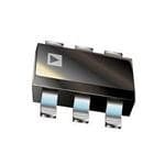
| 产品图片 |
|
| rohs | 符合RoHS无铅 / 符合限制有害物质指令(RoHS)规范要求 |
| 产品系列 | 开关 IC,模拟开关 IC,Analog Devices ADG779BKSZ-R2- |
| 数据手册 | |
| 产品型号 | ADG779BKSZ-R2 |
| 产品种类 | 模拟开关 IC |
| 供应商器件封装 | SC-70-6 |
| 其它名称 | ADG779BKSZ-R2CT |
| 功能 | |
| 包装 | 剪切带 (CT) |
| 商标 | Analog Devices |
| 安装类型 | 表面贴装 |
| 安装风格 | SMD/SMT |
| 导通电阻 | 5 欧姆 |
| 封装 | Reel |
| 封装/外壳 | 6-TSSOP,SC-88,SOT-363 |
| 封装/箱体 | SC-70-6 |
| 工作温度 | -40°C ~ 85°C |
| 工作电源电压 | 5.5 V |
| 工厂包装数量 | 250 |
| 开关数量 | 1 |
| 开关电压—最大值 | 5.5 V |
| 开关配置 | SPDT |
| 最大功率耗散 | 5 uW |
| 最大工作温度 | + 85 C |
| 最小工作温度 | - 40 C |
| 标准包装 | 1 |
| 电压-电源,单/双 (±) | 1.8 V ~ 5.5 V |
| 电压源 | 单电源 |
| 电流-电源 | 1nA |
| 电源电压-最大 | 5.5 V |
| 电源电压-最小 | 0 V |
| 电源电流—最大值 | 1 uA |
| 电路 | 1 x SPDT - NC/NO |
| 空闲时间—最大值 | 3 ns |
| 系列 | ADG779 |
| 运行时间—最大值 | 14 ns |


PDF Datasheet 数据手册内容提取
CMOS 1.8 V to 5.5 V, 2.5 Ω SPDT Switch/2:1 Mux in Tiny SC70 Package ADG779 FEATURES FUNCTIONAL BLOCK DIAGRAM 1.8 V to 5.5 V single supply ADG779 2.5 Ω on resistance S2 0.75 Ω on-resistance flatness D S1 −3 dB bandwidth >200 MHz Rail-to-rail operation IN 6-lead SC70 package FastOt Ns w20it nchs ing times SWIAT CLHOEGSIC S H1 OINWPNU TFOR02491-001 Figure 1. t 6 ns OFF Typical power consumption (<0.01 μW) TTL/CMOS compatible APPLICATIONS Battery-powered systems Communication systems Sample hold systems Audio signal routing Video switching Mechanical reed relay replacements GENERAL DESCRIPTION PRODUCT HIGHLIGHTS The ADG779 is a monolithic CMOS SPDT (single-pole, double-throw) switch. This switch is designed on a submicron 1. Tiny 6-Lead SC70 Package. process that provides low power dissipation yet gives high switching speed, low on resistance, and low leakage currents. 2. 1.8 V to 5.5 V Single-Supply Operation. The ADG779 offers high performance, including low on resistance and The ADG779 operates from a single supply range of 1.8 V to fast switching times, and is fully specified and guaranteed 5.5 V, making it ideal for use in battery-powered instruments with 3 V and 5 V supply rails. and with the new generation of DACs and ADCs from Analog Devices, Inc. 3. Very Low RON (5 Ω max at 5 V, 10 Ω max at 3 V). At 1.8 V operation, R is typically 40 Ω over the temperature range. ON Each switch of the ADG779 conducts equally well in both directions when on. The ADG779 exhibits break-before-make 4. On-Resistance Flatness (RFLAT (ON)) (0.75 Ω typ). switching action. 5. −3 dB Bandwidth > 200 MHz. Because of the advanced submicron process, −3 dB bandwidth 6. Low Power Dissipation. CMOS construction ensures low of greater than 200 MHz can be achieved. power dissipation. The ADG779 is available in a 6-lead SC70 package. 7. 14 ns Switching Times. Rev. A Information furnished by Analog Devices is believed to be accurate and reliable. However, no responsibility is assumed by Analog Devices for its use, nor for any infringements of patents or other One Technology Way, P.O. Box 9106, Norwood, MA 02062-9106, U.S.A. rights of third parties that may result from its use. Specifications subject to change without notice. No license is granted by implication or otherwise under any patent or patent rights of Analog Devices. Tel: 781.329.4700 www.analog.com Trademarks and registered trademarks are the property of their respective owners. Fax: 781.461.3113 © 2005 Analog Devices, Inc. All rights reserved.
ADG779 TABLE OF CONTENTS Features..............................................................................................1 Pin Configuration and Function Descriptions..............................6 Applications.......................................................................................1 Terminology.......................................................................................7 Functional Block Diagram..............................................................1 Typical Performance Characteristics..............................................8 General Description.........................................................................1 Test Circuits.....................................................................................10 Product Highlights...........................................................................1 Outline Dimensions.......................................................................12 Revision History...............................................................................2 Ordering Guide..........................................................................12 Specifications.....................................................................................3 Absolute Maximum Ratings............................................................5 ESD Caution..................................................................................5 REVISION HISTORY 10/05—Rev. 0 to Rev. A Updated Format..................................................................Universal Changes to Table 1............................................................................3 Changes to Table 2............................................................................4 Changes to Table 3............................................................................5 Changes to Terminology Section....................................................7 Changes to Ordering Guide..........................................................12 7/01—Revision 0: Initial Version Rev. A | Page 2 of 12
ADG779 SPECIFICATIONS V = 5 V ± 10%, GND = 0 V1 DD Table 1. B Version −40°C to Parameter 25°C +85°C Unit Test Conditions/Comments ANALOG SWITCH Analog Signal Range 0 V to V V DD On Resistance (R ) 2.5 Ω typ V = 0 V to V , I = −10 mA, see Figure 12 ON S DD S 5 6 Ω max On-Resistance Match Between Channels (ΔR ) 0.1 Ω typ V = 0 V to V , I = −10 mA ON S DD S 0.8 Ω max On-Resistance Flatness (R ) 0.75 Ω typ V = 0 V to V , I = −10 mA FLAT (ON) S DD S 1.2 Ω max LEAKAGE CURRENTS2 V = 5.5 V DD Source Off Leakage I (Off) ±0.01 ±0.05 nA typ V = 4.5 V/1 V, V = 1 V/4.5 V, see Figure 13 S S D Channel On Leakage I , I (On) ±0.01 ±0.05 nA typ V = V = 1 V, or V = V = 4.5 V, see Figure 14 D S S D S D DIGITAL INPUTS Input High Voltage, V 2.4 V min INH Input Low Voltage, V 0.8 V max INL Input Current I or I 0.005 μA typ V = V or V INL INH IN INL INH ±0.1 μA max DYNAMIC CHARACTERISTICS2 t 14 ns typ R = 300 Ω, C = 35 pF ON L L 20 ns max V = 3 V, see Figure 15 S t 3 ns typ R = 300 Ω, C = 35 pF OFF L L 6 ns max V = 3 V, see Figure 15 S Break-Before-Make Time Delay, t 8 ns typ R = 300 Ω, C = 35 pF D L L 1 ns min V = V = 3 V, see Figure 16 S1 S2 Off Isolation −67 dB typ R = 50 Ω, C = 5 pF, f = 10 MHz L L −87 dB typ R = 50 Ω, C = 5 pF, f = 1 MHz, see Figure 17 L L Channel-to-Channel Crosstalk −62 dB typ R = 50 Ω, C = 5 pF, f = 10 MHz L L −82 dB typ R = 50 Ω, C = 5 pF, f = 1 MHz, see Figure 18 L L Bandwidth –3 dB 200 MHz typ R = 50 Ω, C = 5 pF, see Figure 19 L L C (Off) 7 pF typ f = 1 MHz S C , C (On) 27 pF typ f = 1 MHz D S POWER REQUIREMENTS V = 5.5 V DD Digital Inputs = 0 V or 5 V I 0.001 μA typ DD 1.0 μA max 1 Temperature range is B Version, −40°C to +85°C. 2 Guaranteed by design, not subject to production test. Rev. A | Page 3 of 12
ADG779 V = 3 V ± 10%, GND = 0 V1 DD Table 2. B Version −40°C to Parameter 25°C +85°C Unit Test Conditions/Comments ANALOG SWITCH Analog Signal Range 0 V to V V DD On Resistance (R ) 6 7 Ω typ V = 0 V to V , I = –10 mA, see Figure 12 ON S DD S 10 Ω max On-Resistance Match Between Channels (ΔR ) 0.1 Ω typ V = 0 V to V , I = –10 mA ON S DD S 0.8 Ω max On-Resistance Flatness (R ) 2.5 Ω typ V = 0 V to V , I = –10 mA FLAT (ON) S DD S LEAKAGE CURRENTS2 V = 3.3 V DD Source Off Leakage I (Off) ±0.01 ±0.05 nA typ V = 3 V/1 V, V = 1 V/3 V, see Figure 13 S S D Channel On Leakage I , I (On) ±0.01 ±0.05 nA typ V = V = 1 V, or V = V = 3 V, see Figure 14 D S S D S D DIGITAL INPUTS Input High Voltage, V 2.0 V min INH Input Low Voltage, V 0.8 V max INL Input Current I or I 0.005 μA typ V = V or V INL INH IN INL INH ±0.1 μA max DYNAMIC CHARACTERISTICS2 t 16 ns typ R = 300 Ω, C = 35 pF ON L L 24 ns max V = 2 V, see Figure 15 S t 4 ns typ R = 300 Ω, C = 35 pF OFF L L 7 ns max V = 2 V, see Figure 15 S Break-Before-Make Time Delay, t 8 ns typ R = 300 Ω, C = 35 pF D L L 1 ns min V = V = 2 V, see Figure 16 S1 S2 Off Isolation –67 dB typ R = 50 Ω, C = 5 pF, f = 10 MHz L L –87 dB typ R = 50 Ω, C = 5 pF, f = 1 MHz, see Figure 17 L L Channel-to-Channel Crosstalk –62 dB typ R = 50 Ω, C = 5 pF, f = 10 MHz L L –82 dB typ R = 50 Ω, C = 5 pF, f = 1 MHz, see Figure 18 L L Bandwidth −3 dB 200 MHz typ R = 50 Ω, C = 5 pF, see Figure 19 L L C (Off) 7 pF typ f = 1 MHz S C , C (On) 27 pF typ f = 1 MHz D S POWER REQUIREMENTS V = 3.3 V DD Digital Inputs = 0 V or 3 V I 0.001 μA typ DD 1.0 μA max 1 Temperature range is B Version, −40°C to +85°C. 2 Guaranteed by design, not subject to production test. Rev. A | Page 4 of 12
ADG779 ABSOLUTE MAXIMUM RATINGS T = 25°C, unless otherwise noted. A Table 3. Parameter Rating Stresses above those listed under Absolute Maximum Ratings VDD to GND −0.3 V to +7 V may cause permanent damage to the device. This is a stress Analog, Digital Inputs1 −0.3 V to VDD + 0.3 V or 30 mA, rating only; functional operation of the device at these or any whichever occurs first other conditions above those indicated in the operational Peak Current, S or D 100 mA (pulsed at 1 ms, section of this specification is not implied. Exposure to absolute 10% duty cycle max) maximum rating conditions for extended periods may affect Continuous Current, S or D 30 mA device reliability. Operating Temperature Range Industrial (B Version) −40°C to +85°C Storage Temperature Range −65°C to +150°C Junction Temperature 150°C SC70 Package, Power Dissipation 315 mW Table 4. Truth Table θJA Thermal Impedance 332°C/W ADG779 IN Switch S1 Switch S2 θ Thermal Impedance 120°C/W JC 0 On Off Lead Temperature, Soldering 1 Off On Vapor Phase (60 sec) 215°C Infrared (15 sec) 220°C Reflow Soldering (Pb-free) Peak Temperature 260 (+0/−5)°C Time at Peak Temperature 10 sec to 40 sec 1 Overvoltages at IN, S, or D are clamped by internal diodes. Current should be limited to the maximum ratings given. ESD CAUTION ESD (electrostatic discharge) sensitive device. Electrostatic charges as high as 4000 V readily accumulate on the human body and test equipment and can discharge without detection. Although this product features proprietary ESD protection circuitry, permanent damage may occur on devices subjected to high energy electrostatic discharges. Therefore, proper ESD precautions are recommended to avoid performance degradation or loss of functionality. Rev. A | Page 5 of 12
ADG779 PIN CONFIGURATION AND FUNCTION DESCRIPTIONS IN 1 6 S2 ADG779 VDD 2 TOP VIEW 5 D (Not to Scale) GND 3 4 S102491-002 Figure 2. Pin Configuration Table 5. Pin Function Descriptions Pin No. Mnemonic Description 1 IN Logic Control Input. 2 V Most Positive Power Supply Potential. DD 3 GND Ground (0 V) Reference. 4 S1 Source Terminal. Can be an input or an output. 5 D Drain Terminal. Can be an input or an output. 6 S2 Source Terminal. Can be an input or an output. Rev. A | Page 6 of 12
ADG779 TERMINOLOGY V C (Off) DD D Most positive power supply potential. Off switch drain capacitance. Measured with reference to ground. I DD Positive supply current. C , C (On) D S On switch capacitance. Measured with reference to ground. GND Ground (0 V) reference. C IN Digital input capacitance. S Source terminal. Can be an input or an output. t ON Delay time between the 50% and 90% points of the digital input D and switch on condition. Drain terminal. Can be an input or an output. t OFF IN Delay time between the 50% and 90% points of the digital input Logic control input. and switch off condition. V (V) D S t BBM Analog voltage on drain (D) and source (S) terminals. On or off time measured between the 80% points of both switches when switching from one to another. R ON Ohmic resistance between the D and S. Charge Injection A measure of the glitch impulse transferred from the digital R FLAT (ON) input to the analog output during on/off switching. Flatness is defined as the difference between the maximum and minimum value of on resistance as measured. Off Isolation A measure of unwanted signal coupling through an off switch. ΔR ON On-resistance mismatch between any two channels. Crosstalk A measure of unwanted signal that is coupled through from one I (Off) S channel to another because of parasitic capacitance. Source leakage current with the switch off. −3 dB Bandwidth I (Off) D The frequency at which the output is attenuated by 3 dB. Drain leakage current with the switch off. On Response I , I (On) D S The frequency response of the on switch. Channel leakage current with the switch on. Insertion Loss V INL The loss due to the on resistance of the switch. Maximum input voltage for Logic 0. THD + N V INH The ratio of harmonic amplitudes plus noise of a signal to the Minimum input voltage for Logic 1. fundamental. I (I ) INL INH Input current of the digital input. C (Off) S Off switch source capacitance. Measured with reference to ground. Rev. A | Page 7 of 12
ADG779 TYPICAL PERFORMANCE CHARACTERISTICS 6.0 0.15 5.5 VDD=2.7V TA=25°C VVDDD==4.55VV/1V 5.0 VS=1V/4.5V 4.5 0.10 4.0 3.5 VDD=3V VDD=4.5V nA) R (Ω)ON32..05 RRENT ( 0.05 ID,IS(ON) U 2.0 VDD=5V C 1.5 0 1.0 0.5 IS(OFF) 00 0.5VD1 O.0RVS1.–5DRA2.I0N OR2.S5OUR3.C0EVO3.L5TAG4E.0(V)4.5 5.002491-003 –0.050 10 20 30TEMP4E0RATU5R0E(°C6)0 70 80 9002491-006 Figure 3. On Resistance as a Function of VD (VS) Single Supplies Figure 6. Leakage Currents as a Function of Temperature 6.0 0.15 5.5 VDD = 3V VVDDD = =3 V3V/1V 5.0 +85°C VS = 1V/3V 4.5 0.10 +25°C 4.0 –40°C A) 3.5 n Ω) T ( R (ON32..05 RREN 0.05 ID, IS (ON) U C 2.0 1.5 0 1.0 0.5 IS (OFF) 00 V0D.5 OR VS –1 D.0RAIN OR1 .S5OURCE 2V.O0LTAGE 2(.V5) 3.002491-004 –0.050 10 20 30TEMP4E0RATU5R0E (°C6)0 70 80 9002491-007 Figure 4. On Resistance as a Function of VD (VS) for Figure 7. Leakage Currents as a Function of Temperature Different Temperatures VDD = 3 V 6.0 10m 5.5 VDD = 5V VDD = 5V 1m 5.0 4.5 100µ 4.0 (Ω)N33..50 +85°C (A)PLY10µ RO2.5 +25°C SUP 1µ I 2.0 –40°C 100n 1.5 1.0 10n 0.5 00 0.5VD 1O.0R VS1 .–5 DRA2I.N0 OR2 .S5OUR3C.0E VO3.L5TAG4E.0 (V)4.5 5.002491-005 1n1 10 100 1FkREQU1E0NkCY (1H0z0)k 1M 10M 100M02491-008 Figure 5. On Resistance as a Function of VD (VS) for Figure 8. Supply Current vs. Input Switching Frequency Different Temperatures VDD = 5 V Rev. A | Page 8 of 12
ADG779 –30 0 VDD = 5V, 3V –40 –50 VDD = 5V ON (dB) ––7600 SE (dB) –2 TI N A –80 O L P O S OFF IS–1–0900 ON RE –4 –110 –120 –13010k 100k FREQ1UMENCY (Hz) 10M 100M 02491-009 –610k 100k FREQ1UMENCY (Hz) 10M 100M 02491-011 Figure 9. Off Isolation vs. Frequency Figure 11. On Response vs. Frequency –30 VDD = 5V, 3V –40 –50 –60 B) K (d –70 L A –80 T S OS –90 R C –100 –110 –120 –13010k 100k FREQ1UMENCY (Hz) 10M 100M 02491-010 Figure 10. Crosstalk vs. Frequency Rev. A | Page 9 of 12
ADG779 TEST CIRCUITS IDS V1 IS(OFF) ID(OFF) S D S D A A ID(ON) S D A VS RON=V1/IDS 02491-012 VS VD 02491-013 VS VD02491-014 Figure 12. On Resistance Figure 13. Off Leakage Figure 14. On Leakage VDD 0.1µF VIN 50% 50% VDD S D 90% 90% VOUT VOUT VS RL CL IN 300Ω 35pF t t GND ON OFF Figure 15. Switching Times 02491-015 VDD 0.1µF S1 VDD VIN 0V 50% 50% VS1 D D2 VS2 SIN2 R30L02Ω C35Lp2F VOUT VOUT 0V50% 50% VIN GND tD tD 02491-016 Figure 16. Break-Before-Make Time Delay, tD Rev. A | Page 10 of 12
ADG779 VDD VDD 0.1µF 0.1µF NETWORK NETWORK VDD ANALYZER VDD ANALYZER S 50Ω S 50Ω IN 50Ω VS IN VS D D VIN GND R50LΩVOUT VIN GND R50LΩVOUT OFF ISOLATION=20 log VVOSUT 02491-017 INSERTIONLOSS=20 log VOVUOTUWTIWTHITOHUSTWSIWTCITHCH 02491-019 Figure 17. Off Isolation Figure 19. Bandwidth VDD 0.1µF NETWORK ANALYZER VDD S1 VOUT RL 50Ω S2 D R 50Ω 50Ω VS IN GND CHANNEL-TO-CHANNELCROSSTALK=20 log VVOSUT 02491-018 Figure 18. Channel-to-Channel Crosstalk Rev. A | Page 11 of 12
ADG779 OUTLINE DIMENSIONS 2.20 2.00 1.80 1.35 6 5 4 2.40 1.25 2.10 1.15 1 2 3 1.80 PIN 1 0.65 BSC 1.30 BSC 1.00 1.10 0.40 0.90 0.80 0.10 0.70 0.46 0.10 MAX 00..3105 SPLEAANTIENG 00..2028 00..3266 0.10 COPLANARITY COMPLIANT TO JEDEC STANDARDS MO-203-AB Figure 20. 6-Lead Thin Shrink Small Outline Transistor Package [SC70] (KS-6) Dimensions shown in millimeters ORDERING GUIDE Package Model Temperature Range Package Description Option Branding1 ADG779BKS-R2 –40°C to +85°C 6-Lead Thin Shrink Small Outline Transistor Package (SC70) KS-6 SKB ADG779BKS-REEL –40°C to +85°C 6-Lead Thin Shrink Small Outline Transistor Package (SC70) KS-6 SKB ADG779BKS-REEL7 –40°C to +85°C 6-Lead Thin Shrink Small Outline Transistor Package (SC70) KS-6 SKB ADG779BKSZ-R22 –40°C to +85°C 6-Lead Thin Shrink Small Outline Transistor Package (SC70) KS-6 S0M ADG779BKSZ-REEL2 –40°C to +85°C 6-Lead Thin Shrink Small Outline Transistor Package (SC70) KS-6 S0M ADG779BKSZ-REEL72 –40°C to +85°C 6-Lead Thin Shrink Small Outline Transistor Package (SC70) KS-6 S0M 1 Brand on these packages is limited to three characters due to space constraints. 2 Z = Pb-free part. © 2005 Analog Devices, Inc. All rights reserved. Trademarks and registered trademarks are the property of their respective owners. C02491–0–10/05(A) Rev. A | Page 12 of 12
Mouser Electronics Authorized Distributor Click to View Pricing, Inventory, Delivery & Lifecycle Information: A nalog Devices Inc.: ADG779BKSZ-REEL ADG779BKSZ-R2 ADG779BKSZ-REEL7