ICGOO在线商城 > 集成电路(IC) > 接口 - 模拟开关,多路复用器,多路分解器 > ADG749BKSZ-REEL7
 Datasheet下载
- 型号: ADG749BKSZ-REEL7
- 制造商: Analog
- 库位|库存: xxxx|xxxx
- 要求:
| 数量阶梯 | 香港交货 | 国内含税 |
| +xxxx | $xxxx | ¥xxxx |
查看当月历史价格
查看今年历史价格
ADG749BKSZ-REEL7产品简介:
ICGOO电子元器件商城为您提供ADG749BKSZ-REEL7由Analog设计生产,在icgoo商城现货销售,并且可以通过原厂、代理商等渠道进行代购。 ADG749BKSZ-REEL7价格参考。AnalogADG749BKSZ-REEL7封装/规格:接口 - 模拟开关,多路复用器,多路分解器, 1 Circuit IC Switch 2:1 5 Ohm SC-70-6。您可以下载ADG749BKSZ-REEL7参考资料、Datasheet数据手册功能说明书,资料中有ADG749BKSZ-REEL7 详细功能的应用电路图电压和使用方法及教程。
ADG749BKSZ-REEL7 是由 Analog Devices Inc.(ADI)生产的一款接口类模拟开关、多路复用器和多路分解器。以下是其典型的应用场景:

1. 信号路由与切换
   ADG749BKSZ-REEL7 可用于需要对多个模拟信号进行切换的系统中,例如音频或视频信号的路由选择。它支持低导通电阻和宽电源范围,适用于在不同输入/输出之间灵活切换信号。

2. 数据采集系统
   在多通道数据采集系统中,这款器件可以作为多路复用器使用,将多个传感器信号依次传输到一个模数转换器(ADC),从而实现高效的数据采集。

3. 通信设备
   该型号适合用于通信设备中的信号路径控制,例如无线基站、调制解调器或其他需要高频信号切换的场合。它的低电容和快速开关时间特性能够确保信号完整性。

4. 工业自动化与控制
   在工业控制系统中,ADG749BKSZ-REEL7 能够帮助管理复杂的信号网络,比如过程控制中的传感器信号分配或多点监控系统的信号切换。

5. 医疗电子设备
   医疗仪器如心电图机(ECG)、超声波设备等可能需要处理来自多个电极或探头的信号,这种情况下可以利用该芯片完成信号的多路选择与传输。

6. 消费电子产品
   对于需要多种功能集成的小型化产品(如智能手机、平板电脑),此器件可以帮助简化电路设计并减少空间占用,同时保证高性能表现。

总之,ADG749BKSZ-REEL7 凭借其优异的电气特性和紧凑封装形式,在众多领域内都有广泛的应用潜力,尤其适用于需要高精度、低功耗以及小型化解决方案的设计项目。
| 参数 | 数值 |
| 产品目录 | 集成电路 (IC)半导体 |
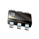
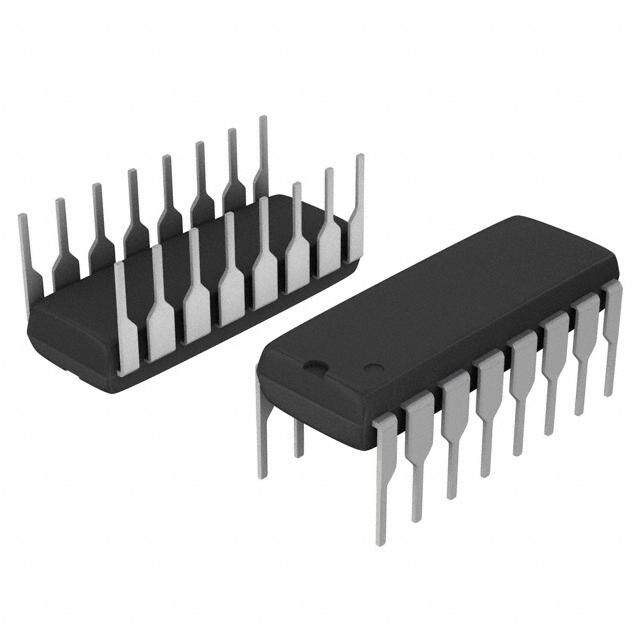
| 描述 | IC SWITCH SPDT SC70-6模拟开关 IC 2.5 Ohm 5.5V CMOS 2:1 Mux/SPDT |
| 产品分类 | |
| 品牌 | Analog Devices |
| 产品手册 | |
| 产品图片 |
|
| rohs | 符合RoHS无铅 / 符合限制有害物质指令(RoHS)规范要求 |
| 产品系列 | 开关 IC,模拟开关 IC,Analog Devices ADG749BKSZ-REEL7- |
| 数据手册 | |
| 产品型号 | ADG749BKSZ-REEL7 |
| 产品培训模块 | http://www.digikey.cn/PTM/IndividualPTM.page?site=cn&lang=zhs&ptm=16843http://www.digikey.cn/PTM/IndividualPTM.page?site=cn&lang=zhs&ptm=16845 |
| 产品目录页面 | |
| 产品种类 | 模拟开关 IC |
| 供应商器件封装 | SC-70-6 |
| 其它名称 | ADG749BKSZ-REEL7DKR |
| 功能 | |
| 包装 | Digi-Reel® |
| 商标 | Analog Devices |
| 安装类型 | 表面贴装 |
| 安装风格 | SMD/SMT |
| 导通电阻 | 5 欧姆 |
| 导通电阻—最大值 | 5 Ohms |
| 封装 | Reel |
| 封装/外壳 | 6-TSSOP,SC-88,SOT-363 |
| 封装/箱体 | SC-70-6 |
| 工作温度 | -40°C ~ 125°C |
| 工作电源电压 | 1.8 V to 5.5 V |
| 工厂包装数量 | 3000 |
| 开关数量 | 1 |
| 开关电压—最大值 | 5.5 V |
| 开关配置 | SPDT |
| 最大功率耗散 | 5 uW |
| 最大工作温度 | + 125 C |
| 最小工作温度 | - 40 C |
| 标准包装 | 1 |
| 电压-电源,单/双 (±) | 1.8 V ~ 5.5 V |
| 电压源 | 单电源 |
| 电流-电源 | 1nA |
| 电源电压-最大 | 5.5 V |
| 电源电压-最小 | 1.8 V |
| 电源电流—最大值 | 1 uA |
| 电路 | 1 x SPDT - NC/NO |
| 空闲时间—最大值 | 6 ns |
| 系列 | ADG749 |
| 运行时间—最大值 | 12 ns |


- 商务部:美国ITC正式对集成电路等产品启动337调查
- 曝三星4nm工艺存在良率问题 高通将骁龙8 Gen1或转产台积电
- 太阳诱电将投资9.5亿元在常州建新厂生产MLCC 预计2023年完工
- 英特尔发布欧洲新工厂建设计划 深化IDM 2.0 战略
- 台积电先进制程称霸业界 有大客户加持明年业绩稳了
- 达到5530亿美元!SIA预计今年全球半导体销售额将创下新高
- 英特尔拟将自动驾驶子公司Mobileye上市 估值或超500亿美元
- 三星加码芯片和SET,合并消费电子和移动部门,撤换高东真等 CEO
- 三星电子宣布重大人事变动 还合并消费电子和移动部门
- 海关总署:前11个月进口集成电路产品价值2.52万亿元 增长14.8%


PDF Datasheet 数据手册内容提取
CMOS 1.8 V to 5.5 V, 2.5 Ω 2:1 Mux/SPDT Switch in SC70 Package Data Sheet ADG749 FEATURES FUNCTIONAL BLOCK DIAGRAM 1.8 V to 5.5 V single supply ADG749 5 Ω (maximum) on resistance S2 0.75 Ω (typical) on resistance flatness D Automotive temperature range: −40°C to +125°C S1 –3 dB bandwidth > 200 MHz Rail-to-rail operation IN 6Fa-lseta sdw SitCc7h0in pga tcikmaegse SAW LOITGCIHC S1H IONPWUNT FOR 02075-001 tON = 12 ns Figure 1. t = 6 ns OFF Typical power consumption (< 0.01 μW) TTL/CMOS compatible APPLICATIONS Battery-powered systems Communication systems Sample-and-hold systems Audio signal routing Video switching Mechanical reed relay replacement GENERAL DESCRIPTION The ADG749 is a monolithic CMOS SPDT switch. This switch PRODUCT HIGHLIGHTS is designed on a submicron process that provides low power 1. 1.8 V to 5.5 V Single-Supply Operation. The ADG749 dissipation yet gives high switching speed, low on resistance, offers high performance, including low on resistance and and low leakage currents. fast switching times, and is fully specified and guaranteed The ADG749 can operate from a single-supply range of 1.8 V to with 3 V and 5 V supply rails. 5.5 V, making it ideal for use in battery-powered instruments 2. Very Low RON (5 Ω Maximum at 5 V and 10 Ω Maximum and with the new generation of DACs and ADCs from Analog at 3 V). At 1.8 V operation, R is typically 40 Ω over the ON Devices, Inc. temperature range. Each switch of the ADG749 conducts equally well in both 3. Automotive Temperature Range: −40°C to +125°C. directions when on. The ADG749 exhibits break-before-make switching action. 4. On Resistance Flatness (RFLAT(ON)) (0.75 Ω typical). 5. −3 dB Bandwidth > 200 MHz. Because of the advanced submicron process, −3 dB bandwidths of greater than 200 MHz can be achieved. 6. Low Power Dissipation. CMOS construction ensures low power dissipation. The ADG749 is available in a 6-lead SC70 package. 7. Fast tON/tOFF. 8. Tiny, 6-lead SC70 Package. Rev. C Information furnished by Analog Devices is believed to be accurate and reliable. However, no responsibility is assumed by Analog Devices for its use, nor for any infringements of patents or other One Technology Way, P.O. Box 9106, Norwood, MA 02062-9106, U.S.A. rights of third parties that may result from its use. Specifications subject to change without notice. No license is granted by implication or otherwise under any patent or patent rights of Analog Devices. Tel: 781.329.4700 www.analog.com Trademarks and registered trademarks are the property of their respective owners. Fax: 781.461.3113 ©2001–2011 Analog Devices, Inc. All rights reserved.
ADG749 Data Sheet TABLE OF CONTENTS Features .............................................................................................. 1 Terminology .......................................................................................7 Applications ....................................................................................... 1 Typical Performance Characteristics ..............................................8 Functional Block Diagram .............................................................. 1 Test Circuits ..................................................................................... 10 General Description ......................................................................... 1 Applications Information .............................................................. 11 Product Highlights ........................................................................... 1 ADG749 Supply Voltages .......................................................... 11 Revision History ............................................................................... 2 On Response vs. Frequency ...................................................... 11 Specifications ..................................................................................... 3 Off Isolation ................................................................................ 11 Absolute Maximum Ratings ............................................................ 5 Outline Dimensions ....................................................................... 12 ESD Caution .................................................................................. 5 Ordering Guide .......................................................................... 12 Pin Configuration and Function Descriptions ............................. 6 REVISION HISTORY 12/11—Rev. B to Rev. C Deleted Endnote 1 from Leakage Currents Parameter, Table 1 . 3 Deleted Endnote 1 from Leakage Currents Parameter, Table 2 . 4 10/09—Rev. A to Rev. B Updated Format .................................................................. Universal Added Pb-Free Information to Table 3 .......................................... 5 Added Table 4 .................................................................................... 6 Updated Outline Dimensions ....................................................... 12 Changes to Ordering Guide .......................................................... 12 7/02—Rev. 0 to Rev. A. Changes to Features .......................................................................... 1 Additions to Product Highlights .................................................... 1 Changes to Specifications ................................................................ 2 Edits to Absolute Maximum Ratings ............................................. 4 Changes to Terminology .................................................................. 4 Edits to Ordering Guide .................................................................. 4 Added new TPCs 4 and 5 ................................................................ 5 Added TPC 10 ................................................................................... 6 Test Circuits 6, 7, and 8 replaced .................................................... 7 Updated KS-6 Package Drawing ..................................................... 9 1/01—Revision 0: Initial Version Rev. C | Page 2 of 12
Data Sheet ADG749 SPECIFICATIONS V = 5 V ± 10% and GND = 0 V; T = −40°C to +125°C unless otherwise stated. DD A Table 1. Parameter 25°C −40°C to +85°C −40°C to +125°C Unit Test Conditions/Comments ANALOG SWITCH Analog Signal Range 0 V to V V DD On Resistance (R ) 2.5 Ω typ V = 0 V to V , I = −10 mA; ON S DD S 5 6 7 Ω max see Figure 13 On Resistance Match Between Channels (ΔR ) 0.1 Ω typ V = 0 V to V , I = −10 mA ON S DD S 0.8 0.8 Ω max On Resistance Flatness (R ) 0.75 Ω typ V = 0 V to V , I = −10 mA FLAT(ON) S DD S 1.2 1.5 Ω max LEAKAGE CURRENTS V = 5.5 V DD Source Off Leakage I (Off) ±0.01 nA typ V = 4.5 V/1 V, V = 1 V/4.5 V; S S D ±0.25 ±0.35 1 nA max see Figure 14 Channel On Leakage I , I (On) ±0.01 nA typ V = V = 1 V or V = V = 4.5 V; D S S D S D ±0.25 ±0.35 5 nA max see Figure 15 DIGITAL INPUTS Input High Voltage, V 2.4 V min INH Input Low Voltage, V 0.8 V max INL Input Current I or I 0.005 μA typ V = V or V INL INH IN INL INH ±0.1 μA max DYNAMIC CHARACTERISTICS1 t 7 ns typ R = 300 Ω, C = 35 pF ON L L 12 ns max V = 3 V; see Figure 16 S t 3 ns typ R = 300 Ω, C = 35 pF OFF L L 6 ns max V = 3 V; see Figure 16 S Break-Before-Make Time Delay, t 8 ns typ R = 300 Ω, C = 35 pF, D L L 1 ns min V = V = 3 V; see Figure 17 S1 S2 Off Isolation −67 dB typ R = 50 Ω, C = 5 pF, f = 10 MHz L L −87 dB typ R = 50 Ω, C = 5 pF, f = 1 MHz; see Figure 18 L L Channel-to-Channel Crosstalk −62 dB typ R = 50 Ω, C = 5 pF, f = 10 MHz L L −82 dB typ R = 50 Ω, C = 5 pF, f = 1 MHz; see Figure 19 L L Bandwidth −3 dB 200 MHz typ R = 50 Ω, C = 5 pF; see Figure 20 L L C (Off) 7 pF typ S C , C (On) 27 pF typ D S POWER REQUIREMENTS V = 5.5 V DD Digital inputs = 0 V or 5.5 V I 0.001 μA typ DD 1.0 μA max 1 Guaranteed by design, not subject to production test. Rev. C | Page 3 of 12
ADG749 Data Sheet V = 3 V ± 10% and GND = 0 V; T = −40°C to +125°C unless otherwise stated DD A Table 2. Parameter 25°C −40°C to +85°C −40°C to +125°C Unit Test Conditions/Comments ANALOG SWITCH Analog Signal Range 0 V to V V DD On Resistance (R ) 6 7 Ω typ V = 0 V to V , I = –10 mA; ON S DD S 10 12 Ω max see Figure 13 On Resistance Match Between Channels (ΔR ) 0.1 Ω typ V = 0 V to V , I = –10 mA ON S DD S 0.8 0.8 Ω max On Resistance Flatness (R ) 2.5 Ω typ V = 0 V to V , I = –10 mA FLAT(ON) S DD S LEAKAGE CURRENTS V = 3.3 V DD Source Off Leakage IS (Off) ±0.01 nA typ V = 3 V/1 V, V = 1 V/3 V; S D ±0.25 ±0.35 1 nA max see Figure 14 Channel On Leakage I , I (On) ±0.01 nA typ V = V = 1 V or V = V = 3 V; D S S D S D ±0.25 ±0.35 5 nA max see Figure 15 DIGITAL INPUTS Input High Voltage, V 2.0 V min INH Input Low Voltage, V 0.8 V max INL Input Current I or I 0.005 μA typ V = V or V INL INH IN INL INH ±0.1 μA max DYNAMIC CHARACTERISTICS1 t 10 ns typ R = 300 Ω, C = 35 pF ON L L 15 ns max V = 2 V; see Figure 16 S t 4 ns typ R = 300 Ω, C = 35 pF OFF L L 8 ns max V = 2 V; see Figure 16 S Break-Before-Make Time Delay, 8 ns typ R = 300 Ω, C = 35 pF L L t D 1 ns min V = V = 2 V; see Figure 17 S1 S2 Off Isolation –67 dB typ R = 50 Ω, C = 5 pF, f = 10 MHz L L –87 dB typ R = 50 Ω, C = 5 pF, f = 1 MHz; see Figure 18 L L Channel-to-Channel Crosstalk –62 dB typ R = 50 Ω, C = 5 pF, f = 10 MHz L L –82 dB typ R = 50 Ω, C = 5 pF, f = 1 MHz; see Figure 19 L L Bandwidth −3 dB 200 MHz typ R = 50 Ω, C = 5 pF; see Figure 20 L L C (Off) 7 pF typ S C , C (On) 27 pF typ D S POWER REQUIREMENTS V = 3.3 V DD Digital inputs = 0 V or 3.3 V I 0.001 μA typ DD 1.0 μA max 1 Guaranteed by design, not subject to production test. Rev. C | Page 4 of 12
Data Sheet ADG749 ABSOLUTE MAXIMUM RATINGS T = 25°C unless otherwise noted. A Table 3. Stresses above those listed under Absolute Maximum Ratings Parameter Ratings may cause permanent damage to the device. This is a stress V to GND −0.3 V to +7 V DD rating only; functional operation of the device at these or any Analog, Digital Input1 −0.3 V to V + 0.3 V or 30 mA, DD other conditions above those indicated in the operational whichever occurs first section of this specification is not implied. Exposure to absolute Peak Current, S or D 100 mA (pulsed at 1 ms, 10% maximum rating conditions for extended periods may affect duty cycle max) device reliability. Continuous Current, S or D 30 mA Operating Temperature Range Only one absolute maximum rating can be applied at any Industrial (B Version) −40°C to +125°C one time. Storage Temperature Range −65°C to +150°C ESD CAUTION Junction Temperature 150°C SC70 Package, Power 315 mW Dissipation θ Thermal Impedance 332°C/W JA θ Thermal Impedance 120°C/W JC Lead Temperature, Soldering Vapor Phase (60 sec) 215°C Infrared (15 sec) 220°C Pb-free Reflow Soldering Peak Temperature 260(+0/–5)°C Time at Peak Temperature 10 sec to 40 sec 1 Overvoltage at IN, S or D will be clamped by internal diodes. Current should be limited to the maximum ratings given. Rev. C | Page 5 of 12
ADG749 Data Sheet PIN CONFIGURATION AND FUNCTION DESCRIPTIONS IN 1 6 S2 ADG749 VDD 2 5 D TOP VIEW GND 3 (Not to Scale) 4 S1 02075-002 Figure 2. Pin Configuration Table 4. Pin Function Descriptions Pin Number Mnemonic Description 1 IN Digital control input pin. 2 V Most positive power supply pin. DD 3 GND Ground (0 V) reference pin. 4 S1 Source terminal of the multiplexer. Can be used as input or output. 5 D Drain terminal of the multiplexer. Can be used as input or output. 6 S2 Source terminal of the multiplexer. Can be used as input or output. Table 5. Truth Table ADG749 IN Switch S1 Switch S2 0 ON OFF 1 OFF ON Rev. C | Page 6 of 12
Data Sheet ADG749 TERMINOLOGY t R ON ON Delay between applying the digital control input and the output Ohmic resistance between D and S. switching on. ΔR ON t On resistance match between any two channels, such as: R OFF ON Delay between applying the digital control input and the output max − R min. ON switching off. R FLAT(ON) t Flatness is defined as the difference between the maximum and D Off time or on time measured between the 90% points of both minimum value of on resistance as measured over the specified switches, when switching from one address state to another. analog signal range. Crosstalk I (Off) S A measure of unwanted signal that is coupled through from one Source leakage current with the switch off. channel to another as a result of parasitic capacitance. I , I (On) D S Off Isolation Channel leakage current with the switch on. A measure of unwanted signal coupling through an off switch. V (V) D S Bandwidth Analog voltage on Terminals D and S. The frequency at which the output is attenuated by −3 dBs. C (Off) S On Response Off switch source capacitance. The frequency response of the on switch. C , C (On) D S On switch capacitance. Insertion Loss Loss due to on resistance of the switch. Rev. C | Page 7 of 12
ADG749 Data Sheet TYPICAL PERFORMANCE CHARACTERISTICS 6.0 0.15 5.5 VDD = 2.7V TA = 25°C VDD = 5V VD = 4.5V/1V 5.0 VS = 1V, 4.5V 4.5 0.10 4.0 3.5 VDD = 3.0V VDD = 4.5V nA) R (Ω)ON 32..05 URRENT ( 0.05 ID, IS (ON) 2.0 VDD = 5.0V C 1.5 0 1.0 0.50 02075-003 –0.05 IS (OFF) 02075-006 0 0.5 1.0 1.5 2.0 2.5 3.0 3.5 4.0 4.5 5.0 0 10 20 30 40 50 60 70 80 90 VD OR VS, DRAIN OR SOURCE VOLTAGE (V) TEMPERATURE (°C) Figure 3. On Resistance vs. VD (VS) Single Supplies Figure 6. Leakage Currents vs. Temperature 6.0 0.15 5.5 VDD = 3V VDD = 3V VD = 3V/1V 5.0 +85°C VS = 1V, 3V 4.5 0.10 +25°C 4.0 –40°C A) 3.5 n R (Ω)ON 32..05 URRENT ( 0.05 ID, IS (ON) C 2.0 1.5 0 1.0 0.50 02075-004 –0.05 IS (OFF) 02075-007 0 0.5 1.0 1.5 2.0 2.5 3.0 0 10 20 30 40 50 60 70 80 90 VD OR VS, DRAIN OR SOURCE VOLTAGE (V) TEMPERATURE (°C) Figure 4. On Resistance vs. VD (VS) for Different Temperature, VDD = 3 V Figure 7. Leakage Currents vs. Temperature 6.0 10m 5.5 VDD = 5V VDD = 5V 1m 5.0 4.5 100µ 4.0 R (Ω)ON 332...055 ++2855°°CC (A)SUPPLY 101µµ I 2.0 –40°C 100n 1.5 1.0 10n 0.50 02075-005 1n 02075-008 0 0.5 1.0 1.5 2.0 2.5 3.0 3.5 4.0 4.5 5.0 1 10 100 1k 10k 100k 1M 10M 100M VD OR VS, DRAIN OR SOURCE VOLTAGE (V) FREQUENCY (Hz) Figure 5. On Resistance vs. VD (VS) for Different Temperatures, VDD = 5 V Figure 8. Supply Current vs. Input Switching Frequency Rev. C | Page 8 of 12
Data Sheet ADG749 –30 0 VDD = 5V, 3V VDD = 5V –40 –50 ON (dB) ––6700 SE (dB) –2 TI N A –80 O L P O S OFF IS –1–0900 ON RE –4 –110 ––112300 02075-009 –6 02075-011 10k 100k 1M 10M 100M 10k 100k 1M 10M 100M FREQUENCY (Hz) FREQUENCY (Hz) Figure 9. Off Isolation vs. Frequency Figure 11. On Response vs. Frequency –30 12 VDD = 5V, 3V –40 10 –50 VDD = 5V 8 –60 B) K (d –70 C) 6 VDD = 3V SSTAL –80 Q (pINJ 4 O –90 R 2 C –100 0 –110 ––112300 02075-010 ––42 02075-012 10k 100k 1M 10M 100M 0 1 2 3 4 5 FREQUENCY (Hz) VS (V) Figure 10. Crosstalk vs. Frequency Figure 12. Charge Injection vs. Source Voltage Rev. C | Page 9 of 12
ADG749 Data Sheet TEST CIRCUITS IDS IS (OFF) ID(OFF) ID(ON) S D S D V1 VS A A VD 02075-014 VS A VD 02075-015 S D VS RON = V1/IDS 02075-013 Figure 13. On Resistance Figure 14. Off Leakage Figure 15. On Leakage VDD 0.1µF VDD VIN 50% 50% S D VOUT 90% 90% VS IN R30L0Ω C35LpF VOUT t t ON OFF GND 02075-016 Figure 16. Switching Times VDD 0.1µF VS1 S1 VDD VIN 0V 50% 50% D2 VOUT VS2 S2 RL2 CL2 VOUT 0V 50% 50% IN 300Ω 35pF t t D D VIN GND 02075-017 Figure 17. Break-Before-Make Time Delay, tD VDD VDD VDD 0.1µF 0.1µF 0.1µF NETWORK NETWORK ANALYZER NETWORK ANALYZER ANALYZER VDD 50Ω VDD VDD 50Ω IN S 50Ω VS VOUT R50LΩ S1 D IN S VS S2 R VIN GNDD R50LΩ VOUT V5S0Ω IN GND 50Ω VIN GNDD R50LΩ VOUT OFF ISOLATION = 20 logVVOSUT 02075-018 CROSSTALK = 20 logVVOSUTCHANNEL-TO-CHANNEL 02075-019 INSERTION LOSS = 20 logVOVUOTU WT IWTHITOHU STW SIWTCITHCH 02075-020 Figure 18. Off Isolation Figure 19. Channel-to-Channel Crosstalk Figure 20. Bandwidth Rev. C | Page 10 of 12
Data Sheet ADG749 APPLICATIONS INFORMATION The ADG749 belongs to Analog Devices’ new family of CMOS zero in the numerator of the transfer function A(s). Because the switches. This series of general-purpose switches has improved switch on resistance is small, this zero usually occurs at high switching times, offering lower on resistance, higher band- frequencies. The bandwidth is a function of the switch output widths, low power consumption, and low leakage currents. capacitance combined with C and the load capacitance. The DS ADG749 SUPPLY VOLTAGES frequency pole corresponding to these capacitances appears in the denominator of A(s). Functionality of the ADG749 extends from 1.8 V to 5.5 V single The dominant effect of the output capacitance, C , causes the supply, which makes it ideal for battery-powered instruments, D pole breakpoint frequency to occur first. Therefore, in order where power efficiency and performance are important design to maximize bandwidth, a switch must have a low input and parameters. output capacitance and low on resistance. The on response vs. It is important to note that the supply voltage affects the input frequency plot for the ADG749 is shown in Figure 11. signal range, the on resistance, and the switching times of the OFF ISOLATION part. By taking a look at the typical performance characteristics and the specifications, the effects of the power supplies can be Off isolation is a measure of the input signal coupled through clearly seen. an off switch to the switch output. The capacitance, C , couples DS the input signal to the output load when the switch is off, as For V = 1.8 V operation, R is typically 40 Ω over the DD ON shown in Figure 22. temperature range. ON RESPONSE VS. FREQUENCY CDS S D Figure 21 illustrates the parasitic components that affect the VOUT asfuucr rptrheoreufrno ddrmeegdar nabdcyee a os bof omCxMe). pOAedSrfd osiwrtimiotcnahnaelc see .x( tTthehrene ssawel icctaacpphaa iccsii ttsaahnnoccweenss awfiflelc t VIN CD CLOAD RLOAD 02075-022 Figure 22. Off Isolation is Affected by External Load Resistance feedthrough, crosstalk, and system bandwidth. and Capacitance CDS The larger the value of CDS, the larger the values of feed- S D through that will be produced. The typical performance VOUT VIN RON CD CLOAD RLOAD 02075-021 ci2sh0oa0lra katiHcotnezr, aitssht eiac s fgwurniatcpcthhio sonhf ooFwfi gfsru ebrqeeut 9tee nirl cltuyhs.a tFnrra o−tem9s5 td hdceB td oisr roooplau tiginoh nolyf. fU p to Figure 21. Switch Represented by Equivalent Parasitic Components frequencies of 10 MHz, the off isolation remains better than The transfer function that describes the equivalent diagram of −67 dB. As the frequency increases, more and more of the input the switch (Figure 21) is of the form A(s) shown below. signal is coupled through to the output. Off isolation can be s(R C )+1 maximized by choosing a switch with the smallest CDS possible. A(s)=R ( ON DS ) The values of load resistance and capacitance also affect off TsRT RON CDS +1 isolation, since they contribute to the coefficients of the poles and zeros in the transfer function of the switch when open. where: ( ) R = R /(R + R ) sR C T LOAD LOAD ON A(s)= ( )( LOAD DS ) CT = CLOAD + CD + CDS s RLOAD CLOAD +CD +CDS +1 The signal transfer characteristic is dependent on the switch channel capacitance, C . This capacitance creates a frequency DS Rev. C | Page 11 of 12
ADG749 Data Sheet OUTLINE DIMENSIONS 2.20 2.00 1.80 1.35 6 5 4 2.40 1.25 2.10 1.15 1 2 3 1.80 0.65BSC 1.30BSC 1.00 1.10 0.40 0.90 0.80 0.10 0.70 0.46 0.10MAX 0.30 SPELAATNIENG 00..2028 0.36 COPLANARITY 0.15 0.26 0.10 COMPLIANTTOJEDECSTANDARDSMO-203-AB 072809-A Figure 23. 6-Lead Thin Shrink Small Outline Transistor Package [SC70] (KS-6) Dimensions shown in millimeters ORDERING GUIDE Model1 Temperature range Package Description Package Option Branding2 ADG749BKSZ-R2 −40°C to +125°C 6-Lead Thin Shrink Small Outline Transistor Package [SC70] KS-6 S1M ADG749BKSZ-REEL −40°C to +125°C 6-Lead Thin Shrink Small Outline Transistor Package [SC70] KS-6 S1M ADG749BKSZ-REEL7 −40°C to +125°C 6-Lead Thin Shrink Small Outline Transistor Package [SC70] KS-6 S1M 1 Z= RoHS Compliant Part. 2 Branding on this package is limited to three characters due to space constraints. ©2001–2011 Analog Devices, Inc. All rights reserved. Trademarks and registered trademarks are the property of their respective owners. D02075-0-12/11(C) Rev. C | Page 12 of 12
Mouser Electronics Authorized Distributor Click to View Pricing, Inventory, Delivery & Lifecycle Information: A nalog Devices Inc.: ADG749BKSZ-REEL ADG749BKSZ-REEL7