ICGOO在线商城 > 集成电路(IC) > 接口 - 模拟开关,多路复用器,多路分解器 > ADG658YRUZ-REEL7
 Datasheet下载
- 型号: ADG658YRUZ-REEL7
- 制造商: Analog
- 库位|库存: xxxx|xxxx
- 要求:
| 数量阶梯 | 香港交货 | 国内含税 |
| +xxxx | $xxxx | ¥xxxx |
查看当月历史价格
查看今年历史价格
ADG658YRUZ-REEL7产品简介:
ICGOO电子元器件商城为您提供ADG658YRUZ-REEL7由Analog设计生产,在icgoo商城现货销售,并且可以通过原厂、代理商等渠道进行代购。 ADG658YRUZ-REEL7价格参考。AnalogADG658YRUZ-REEL7封装/规格:接口 - 模拟开关,多路复用器,多路分解器, 1 Circuit IC Switch 8:1 75Ohm 16-TSSOP。您可以下载ADG658YRUZ-REEL7参考资料、Datasheet数据手册功能说明书,资料中有ADG658YRUZ-REEL7 详细功能的应用电路图电压和使用方法及教程。
ADG658YRUZ-REEL7是Analog Devices Inc.生产的一款CMOS模拟开关,属于接口类器件中的多路复用器/多路分解器。该芯片为16通道单刀双掷(SPDT)配置,采用TSSOP-24封装,支持低电压单电源供电(2.7V至5.5V),具有低导通电阻、低功耗和快速开关速度的特点。

其典型应用场景包括便携式仪表、数据采集系统、工业控制与自动化设备、通信系统以及测试测量仪器。在多通道传感器信号切换中,ADG658YRUZ-REEL7可用于选择不同传感器输入,实现高效模拟信号路由;在音频与视频信号切换系统中,可作为多路信号选择开关,确保信号完整性;在电池供电设备中,得益于其低功耗特性,有助于延长设备续航时间。

此外,该器件具备高隔离度和低串扰性能,适合需要高精度信号处理的应用场合。其工业级温度范围(-40°C至+85°C)使其能在恶劣环境中稳定工作,广泛应用于医疗设备、过程控制及现场仪器等对可靠性要求较高的领域。ADG658YRUZ-REEL7以高集成度和优异的电气性能,成为多路模拟信号管理的理想选择。
| 参数 | 数值 |
| 产品目录 | 集成电路 (IC)半导体 |
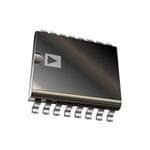
| 描述 | IC MULTIPLEXER 8X1 16TSSOP多路器开关 IC 8:1 210MHz 45 Ohm CMOS |
| 产品分类 | |
| 品牌 | Analog Devices |
| 产品手册 | |
| 产品图片 |
|
| rohs | 符合RoHS无铅 / 符合限制有害物质指令(RoHS)规范要求 |
| 产品系列 | 开关 IC,多路器开关 IC,Analog Devices ADG658YRUZ-REEL7- |
| 数据手册 | |
| 产品型号 | ADG658YRUZ-REEL7 |
| 串话 | 90 dB |
| 产品培训模块 | http://www.digikey.cn/PTM/IndividualPTM.page?site=cn&lang=zhs&ptm=16845 |
| 产品种类 | 多路器开关 IC |
| 供应商器件封装 | 16-TSSOP |
| 关闭隔离—典型值 | 90 dB |
| 其它名称 | ADG658YRUZ-REEL7DKR |
| 功能 | 多路复用器 |
| 包装 | Digi-Reel® |
| 商标 | Analog Devices |
| 安装类型 | 表面贴装 |
| 安装风格 | SMD/SMT |
| 导通电阻 | 150 欧姆 |
| 导通电阻—最大值 | 45 Ohms |
| 封装 | Reel |
| 封装/外壳 | 16-TSSOP(0.173",4.40mm 宽) |
| 封装/箱体 | TSSOP-16 |
| 工作温度 | -40°C ~ 125°C |
| 工作电源电压 | 5 V |
| 工作电源电流 | 1 uA |
| 工厂包装数量 | 1000 |
| 带宽 | 210 MHz |
| 开关数量 | 1 |
| 最大功率耗散 | 10 uW |
| 最大工作温度 | + 125 C |
| 最小工作温度 | - 40 C |
| 标准包装 | 1 |
| 电压-电源,单/双 (±) | 2 V ~ 12 V, ±2 V ~ 6 V |
| 电压源 | 单/双电源 |
| 电流-电源 | 10nA |
| 电路 | 1 x 8:1 |
| 空闲时间—最大值 | 30 ns |
| 系列 | ADG658 |
| 通道数量 | 8 Channel |


- 商务部:美国ITC正式对集成电路等产品启动337调查
- 曝三星4nm工艺存在良率问题 高通将骁龙8 Gen1或转产台积电
- 太阳诱电将投资9.5亿元在常州建新厂生产MLCC 预计2023年完工
- 英特尔发布欧洲新工厂建设计划 深化IDM 2.0 战略
- 台积电先进制程称霸业界 有大客户加持明年业绩稳了
- 达到5530亿美元!SIA预计今年全球半导体销售额将创下新高
- 英特尔拟将自动驾驶子公司Mobileye上市 估值或超500亿美元
- 三星加码芯片和SET,合并消费电子和移动部门,撤换高东真等 CEO
- 三星电子宣布重大人事变动 还合并消费电子和移动部门
- 海关总署:前11个月进口集成电路产品价值2.52万亿元 增长14.8%


PDF Datasheet 数据手册内容提取
+3 V/+5 V/±5 V, CMOS, 8-Channel Analog Multiplexer Enhanced Product ADG658-EP FEATURES FUNCTIONAL BLOCK DIAGRAM ±2 V to ±6 V dual supply ADG658-EP 2 V to 12 V single supply <0.1 nA leakage currents (typical) S1 45 Ω typical on resistance over full signal range Rail-to-rail switching operation Single, 8 to 1 multiplexer D 16-lead TSSOP package 0.01 μA typical supply current TTL/CMOS compatible inputs S8 ENHANCED PRODUCT FEATURES 1 OF 8 DECODER Supports defense and aerospace applications (AQEC standard) Military temperature range: −55°C to +125°C SWITCHES SAH0OWAN1 FOAR2 A LEONGIC 1 INPUT. 15981-001 Controlled manufacturing baseline Figure 1. One assembly/test site GENERAL DESCRIPTION One fabrication site Enhanced product change notification The ADG658-EP is a low voltage, CMOS analog multiplexer Qualification data available on request comprised of eight single channels. The ADG658-EP switches one APPLICATIONS of eight inputs (S1 to S8) to a common output, D, as determined by the 3-bit binary address lines A0, A1, and A2. An EN input enables Automatic test equipment or disables the device. When disabled, all channels are switched off. Data acquisition systems Battery-powered systems The ADG658-EP is designed on an enhanced process that provides Communication systems lower power dissipation yet gives high switching speeds. It can Audio and video signal routing operate equally well as either a multiplexer or a demultiplexer, and Relay replacement has an input range that extends to the supplies. All channels exhibit Sample-and-hold systems break-before-make switching action, preventing momentary Industrial control systems shorting when switching channels. All digital inputs have +0.8 V to +2.4 V logic thresholds, ensuring TTL/CMOS logic compatibi- lity when using single +5 V or dual ±5 V supplies. The ADG658-EP is available in a 16-lead TSSOP package. Additional application and technical information can be found in the ADG658 data sheet. PRODUCT HIGHLIGHTS 1. Single-supply and dual-supply operation. The ADG658-EP offers high performance and is fully specified and guaranteed with ±5 V, +5 V, and +3 V supply rails. 2. Military temperature range −55°C to +125°C. 3. Low supply current, typically 0.01 µA. 4. 16-lead TSSOP package. Rev. 0 Document Feedback Information furnished by Analog Devices is believed to be accurate and reliable. However, no responsibility is assumed by Analog Devices for its use, nor for any infringements of patents or other One Technology Way, P.O. Box 9106, Norwood, MA 02062-9106, U.S.A. rights of third parties that may result from its use. Specifications subject to change without notice. No license is granted by implication or otherwise under any patent or patent rights of Analog Devices. Tel: 781.329.4700 ©2017 Analog Devices, Inc. All rights reserved. Trademarks and registered trademarks are the property of their respective owners. Technical Support www.analog.com
ADG658-EP Enhanced Product TABLE OF CONTENTS Features .............................................................................................. 1 5 V Single Supply ...........................................................................3 Enhanced Product Features ............................................................ 1 2.7 V to 3.6 V Single Supply .........................................................5 Applications ....................................................................................... 1 Absolute Maximum Ratings ............................................................6 Functional Block Diagram .............................................................. 1 ESD Caution...................................................................................6 General Description ......................................................................... 1 Pin Configurations and Function Descriptions ............................7 Product Highlights ........................................................................... 1 Typical Performance Characteristics ..............................................8 Revision History ............................................................................... 2 Outline Dimensions ....................................................................... 10 Specifications ..................................................................................... 3 Ordering Guide .......................................................................... 10 Dual Supply ................................................................................... 3 REVISION HISTORY 8/2017—Revision 0: Initial Version Rev. 0 | Page 2 of 10
Enhanced Product ADG658-EP SPECIFICATIONS DUAL SUPPLY V = 5 V ± 10%, V = −5 V ± 10%, GND = 0 V, unless otherwise noted. DD SS Table 1. −55°C to Parameter +25°C +125°C Unit Test Conditions/Comments ANALOG SWITCH Analog Signal Range V to V V V = +4.5 V, V = −4.5 V SS DD DD SS On Resistance, R 45 Ω typ Source voltage (V) = ±4.5 V, source current (I) = 1 mA ON S S 75 100 Ω max On Resistance Match Between 1.3 Ω typ Channels, ∆R 3 3.5 Ω max V = 3.5 V, I = 1 mA ON S S On Resistance Flatness, R 10 Ω typ V = +5 V, V = −5 V FLAT(ON) DD SS 16 18 Ω max V = ±3 V, I = 1 mA S S LEAKAGE CURRENTS V = +5.5 V, V = −5.5 V DD SS Source Off Leakage, IS (OFF) ±0.005 nA typ Drain voltage (VD) = ±4.5 V, VS = 4.5 V ±0.2 ±5 nA max Drain Off Leakage, ID (OFF) ±0.005 nA typ VD = ±4.5 V, VS = 4.5 V ±0.2 ±5 nA max Channel On Leakage I , I (ON) ±0.005 nA typ V = V = ±4.5 V D S D S ±0.2 ±5 nA max DIGITAL INPUTS Input High Voltage, V 2.4 V min INH Input Low Voltage, V 0.8 V max INL Input Current I or I 0.005 µA typ Input voltage (V ) = V or V INL INH IN INL INH ±1 µA max Digital Input Capacitance, C 2 pF typ IN DYNAMIC CHARACTERISTICS1 Transition Time, t 80 ns typ Load resistance (R) = 300 Ω, load capacitance (C) = 35 pF TRANSITION L L 115 165 ns max V = 3 V S EN On Time, tON (EN) 80 ns typ RL = 300 Ω, CL = 35 pF 115 165 ns max V = 3 V S EN Off Time, tOFF (EN) 30 ns typ RL = 300 Ω, CL = 35 pF 45 55 ns max V = 3 V S Break-Before-Make Time Delay, t 50 ns typ R = 300 Ω, C = 35 pF BBM L L 10 ns min Source 1 voltage (V ) = 3 V, source 2 voltage (V ) = 3 V S1 S2 Charge Injection 2 pC typ V = 0 V, R = 0 Ω S S 4 pC max C = 1 nF L Off Isolation −90 dB typ R = 50 Ω, C = 5 pF, f = 1 MHz L L Total Harmonic Distortion Plus Noise, THD + N 0.025 % typ R = 600 Ω, 2 V p-p, f = 20 Hz to 20 kHz L −3 dB Bandwidth 210 MHz R = 50 Ω, C = 5 pF L L typ Source Capacitance, C (OFF) 4 pF typ f = 1 MHz S Drain Capacitance, C (OFF) 23 pF typ f = 1 MHz D C , C (ON) 28 pF typ f = 1 MHz D S POWER REQUIREMENTS V = +5.5 V, V = −5.5 V DD SS Positive Power Supply Current, I 0.01 µA typ Digital inputs = 0 V or 5.5 V DD 1 µA max Negative Power Supply Current, I 0.01 µA typ Digital inputs = 0 V or 5.5 V SS 1 µA max 1 Guaranteed by design; not subject to production test. Rev. 0 | Page 3 of 10
ADG658-EP Enhanced Product 5 V SINGLE SUPPLY V = 5 V ± 10%, V = 0 V, GND = 0 V, unless otherwise noted. DD SS Table 2. Parameter +25°C −55°C to +125°C Unit Test Conditions/Comments ANALOG SWITCH Analog Signal Range 0 to V V V = 4.5 V, V = 0 V DD DD SS On Resistance, R 85 Ω typ V = 0 V to 4.5 V, I = 1 mA ON S S 150 200 Ω max On Resistance Match Between 4.5 Ω typ V = 3.5 V, I = 1 mA S S Channels, ∆R 8 10 Ω max ON On Resistance Flatness, R 13 16 Ω typ V = 5 V, V = 0 V, V = 1.5 V to 4 V, I = 1 mA FLAT(ON) DD SS S S LEAKAGE CURRENTS V = 5.5 V DD Source Off Leakage, I (OFF) ±0.005 nA typ V = 1 V/4.5 V, V = 4.5 V/1 V S S D ±0.2 ±5 nA max Drain Off Leakage, I (OFF) ±0.005 nA typ V = 1 V/4.5 V, V = 4.5 V/1 V D S D ±0.2 ±5 nA max Channel On Leakage I , I (ON) ±0.005 nA typ V = V = 1 V or 4.5 V D S S D ±0.2 ±5 nA max DIGITAL INPUTS Input High Voltage, V 2.4 V min INH Input Low Voltage, V 0.8 V max INL Input Current I or I 0.005 µA typ V = V or V INL INH IN INL INH ±1 µA max Digital Input Capacitance, C 2 pF typ IN DYNAMIC CHARACTERISTICS1 Transition Time, t 120 ns typ R = 300 Ω, C = 35 pF TRANSITION L L 200 300 ns max V = 3 V S EN On Time, tON (EN) 120 ns typ RL = 300 Ω, CL = 35 pF 190 280 ns max V = 3 V S EN Off Time, tOFF (EN) 35 ns typ RL = 300 Ω, CL = 35 pF 50 70 ns max V = 3 V S Break-Before-Make Time Delay, t 100 ns typ R = 300 Ω, C = 35 pF BBM L L 10 ns min V = V = 3 V S1 S2 Charge Injection 0.5 pC typ V = 2.5 V, R = 0 Ω, C = 1 nF S S L 1 pC max Off Isolation −90 dB typ R = 50 Ω, C = 5 pF, f = 1 MHz L L −3 dB Bandwidth 180 MHz typ R = 50 Ω, C = 5 pF L L Source Capacitance, C (OFF) 5 pF typ f = 1 MHz S Drain Capacitance, C (OFF) 29 pF typ f = 1 MHz D C , C (ON) 30 pF typ f = 1 MHz D S POWER REQUIREMENTS V = 5.5 V DD Positive Power Supply Current, I 0.01 µA typ Digital inputs = 0 V or 5.5 V DD 1 µA max 1 Guaranteed by design; not subject to production test. Rev. 0 | Page 4 of 10
Enhanced Product ADG658-EP 2.7 V TO 3.6 V SINGLE SUPPLY V = 2.7 to 3.6 V, V = 0 V, GND = 0 V, unless otherwise noted. DD SS Table 3. Parameter +25°C −55°C to +125°C Unit Test Conditions/Comments ANALOG SWITCH Analog Signal Range 0 to V V V = 2.7 V, V = 0 V DD DD SS On Resistance, R 185 Ω typ V = 0 V to 2.7 V, I = 0.1 mA ON S S 300 400 Ω max On Resistance Match Between 2 Ω typ V = 1.5 V, I = 0.1 mA S S Channels, ∆R 4.5 7 Ω max ON LEAKAGE CURRENTS V = 3.3 V DD Source Off Leakage, I (OFF) ±0.005 nA typ V = 1 V/3 V, V = 3 V/1 V S S D ±0.2 ±5 nA max Drain Off Leakage, I (OFF) ±0.005 nA typ V = 1 V/3 V, V = 3 V/1 V D S D ±0.2 ±5 nA max Channel On Leakage I , I (ON) ±0.005 nA typ V = V = 1 V or 3 V D S S D ±0.2 ±5 nA max DIGITAL INPUTS Input High Voltage, V 2.0 V min INH Input Low Voltage, V 0.5 V max INL Input Current I or I 0.005 µA typ V = V or V INL INH IN INL INH ±1 µA max Digital Input Capacitance, C 2 pF typ IN DYNAMIC CHARACTERISTICS1 Transition Time, t 200 ns typ R = 300 Ω, C = 35 pF TRANSITION L L 370 490 ns max V = 1.5 V S EN On Time, tON (EN) 230 ns typ RL = 300 Ω, CL = 35 pF 370 490 ns max V = 1.5 V S EN Off Time, tOFF (EN) 50 ns typ RL = 300 Ω, CL = 35 pF 80 110 ns max V = 1.5 V S Break-Before-Make Time Delay, t 200 ns typ R = 300 Ω, C = 35 pF BBM L L 10 ns min V = V = 1.5 V S1 S2 Charge Injection 1 pC typ V = 1.5 V, R = 0 Ω, C = 1 nF S S L 2 pC max Off Isolation −90 dB typ R = 50 Ω, C = 5 pF, f = 1 MHz L L −3 dB Bandwidth 160 MHz typ R = 50 Ω, C = 5 pF L L Source Capacitance, C (OFF) 5 pF typ f = 1 MHz S Drain Capacitance, C (OFF) 29 pF typ f = 1 MHz D C , C (ON) 30 pF typ f = 1 MHz D S POWER REQUIREMENTS V = 3.6 V DD Positive Power Supply Current, I 0.01 µA typ Digital inputs = 0 V or 3.6 V DD 1 µA max 1 Guaranteed by design; not subject to production test. Rev. 0 | Page 5 of 10
ADG658-EP Enhanced Product ABSOLUTE MAXIMUM RATINGS T = 25°C, unless otherwise noted. Stresses at or above those listed under Absolute Maximum A Ratings may cause permanent damage to the product. This is a Table 4. stress rating only; functional operation of the product at these Parameter Rating or any other conditions above those indicated in the operational V to V 13 V DD SS section of this specification is not implied. Operation beyond V to GND −0.3 V to +13 V DD the maximum operating conditions for extended periods may V to GND +0.3 V to −6.5 V SS affect product reliability. Analog Inputs1 V − 0.3 V to V + 0.3 V SS DD Digital Inputs1 GND − 0.3 V to V + 0.3 V DD or 10 mA, whichever ESD CAUTION occurs first Peak Current, Sx or D 40 mA (Pulsed at 1 ms, 10% duty cycle max) Continuous Current, Sx or D 20 mA Operating Temperature Range −55°C to +125°C Storage Temperature Range −65°C to +150°C Junction Temperature 150°C θ Thermal Impedance JA 16-Lead TSSOP 150.4°C/W Lead Temperature, Soldering Vapor Phase (60 sec) 215°C Infrared (15 sec) 220°C ESD (Human Body Model) 4.0 kV 1 Overvoltages at AX, EN, Sx, or D are clamped by internal diodes. Current must be limited to the maximum ratings. Table 5. Truth Table A2 A1 A0 EN Switch Condition X1 X1 X1 1 None 0 0 0 0 1 0 0 1 0 2 0 1 0 0 3 0 1 1 0 4 1 0 0 0 5 1 0 1 0 6 1 1 0 0 7 1 1 1 0 8 1 X means don’t care Rev. 0 | Page 6 of 10
Enhanced Product ADG658-EP PIN CONFIGURATION AND FUNCTION DESCRIPTIONS S5 1 16 VDD S7 2 15 S3 D 3 14 S2 S8 4 ADG658-EP 13 S1 TOP VIEW S6 5 (Not to Scale) 12 S4 EN 6 11 A0 VSS 7 10 A1 GND 8 9 A2 15981-002 Figure 2. 16-Lead TSSOP Pin Configuration Table 6. 16-Lead TSSOP Pin Function Descriptions Pin No. Mnemonic Description 1, 2, 4, 5, 12, 13, S1 to S8 Source Terminals. Can be an input or output. 14, 15 3 D Drain Terminal. Can be an input or output. 6 EN Active Low Digital Input. When high, device is disabled and all switches are off. When low, Ax logic inputs determine on switch. 7 V Most Negative Power Supply Potential. SS 8 GND Ground (0 V) Reference. 9, 10, 11 A0 to A2 Logic Control Inputs. 16 V Most Positive Power Supply Potential. DD Rev. 0 | Page 7 of 10
ADG658-EP Enhanced Product TYPICAL PERFORMANCE CHARACTERISTICS 100 1.5 90 1.0 80 IS (OFF) A) 0.5 E (Ω) 70 NT (n 0 C 60 E N R A +125°C +85°C R ST 50 CU –0.5 ON RESI 4300 +–4205°°CC EAKAGE –1.0 ID (OIND) ,( OISF (FO)N) –55°C L –1.5 20 VDD = +5V –2.0 VSS = –5V 10 VD = ±4V VS = ±4V 0–5 –4 –3 –2 –1VD, V0S (V)1 2 3 4 5 15981-003 –2.50 20 40TEMPER60ATURE (°8C0) 100 120 15981-006 Figure 3. On Resistance vs. VD (VS) for Different Temperatures (Dual Supply) Figure 6. Leakage Current vs. Temperature (Dual Supply) 140 1.5 VDD = +5V 120 1.0 VVVSDSS == = ± ± 014VVV IS (OFF) E (Ω) 100 ++18255°°CC NT (nA) 0.50 C E N 80 +25°C R A R ESIST 60 –40°C GE CU –0.5 ID (OFF) N R –55°C KA –1.0 O 40 EA ID (ON), IS (ON) L –1.5 20 –2.0 00 0.5 1.0 1.5 2.0VD, 2V.5S (V)3.0 3.5 4.0 4.5 5.0 15981-004 –2.50 20 40TEMPER60ATURE (°8C0) 100 120 15981-007 Figure 4. On Resistance vs. VD (VS) for Different Temperatures (Single Supply) Figure 7. Leakage Current vs. Temperature (Single Supply) 300 250 +125°C +85°C E (Ω) 200 +25°C C N A ST 150 –40°C SI E –55°C R N 100 O 50 0 0 0.5 1.0 VD, 1V.5S (V) 2.0 2.5 3.0 15981-005 Figure 5. On Resistance vs. VD (VS) for Different Temperatures (Single Supply) Rev. 0 | Page 8 of 10
Enhanced Product ADG658-EP 140 350 VDD = +5V VSS = 0V VSS = –5V 120 300 VDD = 3V 100 250 tON s) 80 s) 200 n n ME ( ME ( VDD = 5V TI 60 TI 150 tON 40 100 VDD = 3V tOFF 20 50 tOFF VDD = 5V 0–55 –35 –15 5TEMP2E5RATU4R5E (°C6)5 85 105 125 15981-008 0–55 –35 –15 5TEMP2E5RATU4R5E (°C6)5 85 105 125 15981-009 Figure 8. tON/tOFF Time vs. Temperature (Dual Supply) Figure 9. tON/tOFF Time vs. Temperature (Single Supply) Rev. 0 | Page 9 of 10
ADG658-EP Enhanced Product OUTLINE DIMENSIONS 5.10 5.00 4.90 16 9 4.50 6.40 4.40 BSC 4.30 1 8 PIN 1 1.20 MAX 0.15 0.20 0.05 0.09 0.75 0.30 8° 0.60 0.65 0.19 SEATING 0° 0.45 BSC PLANE COPLANARITY 0.10 COMPLIANT TO JEDEC STANDARDS MO-153-AB Figure 10. 16-Lead Thin Shrink Small Outline Package [TSSOP] (RU-16) Dimensions shown in millimeters ORDERING GUIDE Model1 Temperature Range Package Description Package Option ADG658TRUZ-EP −55°C to +125°C 16-Lead Thin Shrink Small Outline Package [TSSOP] RU-16 ADG658TRUZ-EP-RL7 −55°C to +125°C 16-Lead Thin Shrink Small Outline Package [TSSOP] RU-16 1 Z = RoHS Compliant Part. ©2017 Analog Devices, Inc. All rights reserved. Trademarks and registered trademarks are the property of their respective owners. D15981-0-8/17(0) Rev. 0 | Page 10 of 10
Mouser Electronics Authorized Distributor Click to View Pricing, Inventory, Delivery & Lifecycle Information: A nalog Devices Inc.: ADG659YRQZ ADG658YCPZ ADG659YCPZ ADW54003-0RL7 ADG659WYRUZ-REEL7 ADG659YRU ADG658YRUZ-REEL7 ADG658YCPZ-REEL7 ADG658YRU-REEL7 ADG659YRUZ-REEL7 ADG658YRQZ-REEL7 ADG659YRUZ ADG659YCPZ-REEL7 ADG658YRU ADW54003-0 ADG658YRUZ ADG658YRQZ ADG658YRQ ADG658TRUZ-EP ADG658TRUZ-EP-RL7