ICGOO在线商城 > 集成电路(IC) > 逻辑 - 信号开关,多路复用器,解码器 > ADG3245BCPZ
 Datasheet下载
- 型号: ADG3245BCPZ
- 制造商: Analog
- 库位|库存: xxxx|xxxx
- 要求:
| 数量阶梯 | 香港交货 | 国内含税 |
| +xxxx | $xxxx | ¥xxxx |
查看当月历史价格
查看今年历史价格
ADG3245BCPZ产品简介:
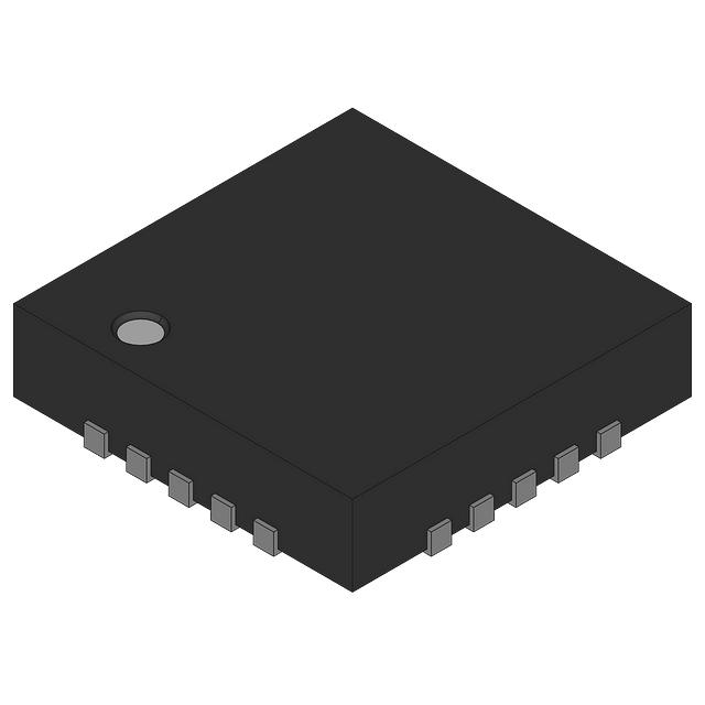
ICGOO电子元器件商城为您提供ADG3245BCPZ由Analog设计生产,在icgoo商城现货销售,并且可以通过原厂、代理商等渠道进行代购。 ADG3245BCPZ价格参考¥8.69-¥18.93。AnalogADG3245BCPZ封装/规格:逻辑 - 信号开关,多路复用器,解码器, Bus Switch 8 x 1:1 20-LFCSP-WQ (4x4)。您可以下载ADG3245BCPZ参考资料、Datasheet数据手册功能说明书,资料中有ADG3245BCPZ 详细功能的应用电路图电压和使用方法及教程。
ADG3245BCPZ 是由 Analog Devices Inc. 生产的一款逻辑信号开关/多路复用器芯片,常用于需要高速信号切换和多通道数据选择的应用场景。该芯片具有低导通电阻、高速切换和宽电源电压范围等优点,适用于多种工业、通信和消费类电子产品。

典型应用场景包括:

1. 数据采集系统:在多通道传感器信号采集系统中,作为多路复用器轮流选择不同传感器信号输入至ADC。

2. 通信系统:用于信号路由和通道选择,如在多路通信接口中切换不同数据通道。

3. 工业控制设备:在PLC或自动化控制系统中实现信号路径的动态切换与管理。

4. 测试与测量设备:用于多路信号的自动切换,提高测试效率,如在示波器或多用表中选择不同输入信号。

5. 音频与视频信号切换:在需要多路音视频信号选择的设备中作为信号开关使用。

6. 嵌入式系统:用于扩展GPIO功能或实现多外设共享同一数据通道。

ADG3245BCPZ采用TSSOP封装,适合在空间受限的电路板上使用,且具备良好的电气性能和稳定性,适合中高精度与中高速度要求的应用场景。
| 参数 | 数值 |
| 产品目录 | 集成电路 (IC)半导体 |
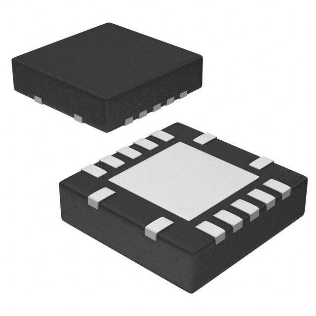
| 描述 | IC SW BUS 2.5-3.3V 8BIT 20LFCSP转换 - 电压电平 2.5V/3.3V 8-Bit 2-Port Bus Switch |
| 产品分类 | |
| 品牌 | Analog Devices |
| 产品手册 | |
| 产品图片 |
|
| rohs | 符合RoHS无铅 / 符合限制有害物质指令(RoHS)规范要求 |
| 产品系列 | 逻辑集成电路,转换 - 电压电平,Analog Devices ADG3245BCPZ- |
| 数据手册 | |
| 产品型号 | ADG3245BCPZ |
| 产品种类 | 转换 - 电压电平 |
| 传播延迟时间 | 225 ps |
| 供应商器件封装 | 20-LFCSP-VQ(4x4) |
| 包装 | 托盘 |
| 商标 | Analog Devices |
| 安装类型 | 表面贴装 |
| 安装风格 | SMD/SMT |
| 封装 | Tray |
| 封装/外壳 | 20-VFQFN 裸露焊盘,CSP |
| 封装/箱体 | LFCSP-20 |
| 工作温度 | -40°C ~ 85°C |
| 工厂包装数量 | 490 |
| 最大工作温度 | + 85 C |
| 最小工作温度 | - 40 C |
| 标准包装 | 490 |
| 独立电路 | 1 |
| 电压-电源 | 2.3 V ~ 3.6 V |
| 电压源 | 单电源 |
| 电流-输出高,低 | - |
| 电源电压-最大 | 3.6 V |
| 电源电压-最小 | 2.3 V |
| 电源电流 | 1 uA |
| 电路 | 8 x 1:1 |
| 类型 | FET 总线开关 |
| 系列 | ADG3245 |


- 商务部:美国ITC正式对集成电路等产品启动337调查
- 曝三星4nm工艺存在良率问题 高通将骁龙8 Gen1或转产台积电
- 太阳诱电将投资9.5亿元在常州建新厂生产MLCC 预计2023年完工
- 英特尔发布欧洲新工厂建设计划 深化IDM 2.0 战略
- 台积电先进制程称霸业界 有大客户加持明年业绩稳了
- 达到5530亿美元!SIA预计今年全球半导体销售额将创下新高
- 英特尔拟将自动驾驶子公司Mobileye上市 估值或超500亿美元
- 三星加码芯片和SET,合并消费电子和移动部门,撤换高东真等 CEO
- 三星电子宣布重大人事变动 还合并消费电子和移动部门
- 海关总署:前11个月进口集成电路产品价值2.52万亿元 增长14.8%


PDF Datasheet 数据手册内容提取
2.5 V/3.3 V, 8-Bit, 2-Port Level Translating, Bus Switch ADG3245 FEATURES FUNCTIONAL BLOCK DIAGRAM 225 ps Propagation Delay through the Switch 4.5 (cid:2) Switch Connection between Ports A0 B0 Data Rate 1.244 Gbps 2.5 V/3.3 V Supply Operation Selectable Level Shifting/Translation Level Translation 3.3 V to 2.5 V 3.3 V to 1.8 V A7 B7 2.5 V to 1.8 V Small Signal Bandwidth 610 MHz 20-Lead TSSOP and LFCSP Packages APPLICATIONS BE 3.3 V to 1.8 V Voltage Translation 3.3 V to 2.5 V Voltage Translation 2.5 V to 1.8 V Voltage Translation Bus Switching Bus Isolation Hot Swap Hot Plug Analog Switch Applications GENERAL DESCRIPTION PRODUCT HIGHLIGHTS The ADG3245 is a 2.5 V or 3.3 V, 8-bit, 2-port digital switch. 1. 3.3 V or 2.5 V supply operation It is designed on Analog Devices’ low voltage CMOS process, 2. Extremely low propagation delay through switch which provides low power dissipation yet gives high switching 3. 4.5 W switches connect inputs to outputs speed and very low on resistance, allowing inputs to be connected 4. Level/voltage translation to outputs without additional propagation delay or generating 5. 20-lead TSSOP and LFCSP (4 mm ¥ 4 mm) packages additional ground bounce noise. The switches are enabled by means of the bus enable (BE) input signal. These digital switches allow bidirectional signals to be switched when ON. In the OFF condition, signal levels up to the supplies are blocked. This device is ideal for applications requiring level translation. When operated from a 3.3 V supply, level translation from 3.3 V inputs to 2.5 V outputs is allowed. Similarly, if the device is operated from a 2.5 V supply and 2.5 V inputs are applied, the device will translate the outputs to 1.8 V. In addition to this, a level translating select pin (SEL) is included. When SEL is low, V is reduced internally, allowing for level translation between CC 3.3 V inputs and 1.8 V outputs. This makes the device suited to applications requiring level translation between different supplies, such as converter to DSP/microcontroller interfacing. Rev. C Document Feedback Information furnished by Analog Devices is believed to be accurate and reliable. However, no responsibility is assumed by Analog Devices for its use, nor for any infringements of patents or other One Technology Way, P.O. Box 9106, Norwood, MA 02062-9106, U.S.A. rights of third parties that may result from its use. Specifications subject to change without notice. No license is granted by implication or otherwise under any patent or patent rights of Analog Devices. Tel: 781.329.4700 ©2003–2015 Analog Devices, Inc. All rights reserved. Trademarks and registered trademarks are the property of their respective owners. Technical Support www.analog.com
ADG3245–SPECIFICATIONS1 (V = 2.3 V to 3.6 V, GND = 0 V, all specifications T to T , unless CC MIN MAX otherwise noted.) B Version Parameter Symbol Conditions Min Typ2 Max Unit DC ELECTRICAL CHARACTERISTICS Input High Voltage V V = 2.7 V to 3.6 V 2.0 V INH CC V V = 2.3 V to 2.7 V 1.7 V INH CC Input Low Voltage V V = 2.7 V to 3.6 V 0.8 V INL CC V V = 2.3 V to 2.7 V 0.7 V INL CC Input Leakage Current I ±0.01 ±1 mA I OFF State Leakage Current I 0 £ A, B £ V ±0.01 ±1 mA OZ CC ON State Leakage Current 0 £ A, B £ V ±0.01 ±1 mA CC Maximum Pass Voltage V V /V = V = SEL = 3.3 V, I = –5 mA 2.0 2.5 2.9 V P A B CC O V /V = V = SEL = 2.5 V, I = –5 mA 1.5 1.8 2.1 V A B CC O V /V = V = 3.3 V, SEL = 0 V, I = –5 mA 1.5 1.8 2.1 V A B CC O CAPACITANCE3 A Port Off Capacitance C OFF f = 1 MHz 5 pF A B Port Off Capacitance C OFF f = 1 MHz 5 pF B A, B Port On Capacitance C , C ON f = 1 MHz 10 pF A B Control Input Capacitance C f = 1 MHz 6 pF IN SWITCHING CHARACTERISTICS3 Propagation Delay A to B or B to A, t 4 t , t C = 50 pF, V = SEL = 3 V 0.225 ns PD PHL PLH L CC Propagation Delay Matching5 22.5 ps Bus Enable Time BE to A or B6 t , t V = 3.0 V to 3.6 V; SEL = V 1 3.2 4.8 ns PZH PZL CC CC Bus Disable Time BE to A or B6 t , t V = 3.0 V to 3.6 V; SEL = V 1 3.2 4.8 ns PHZ PLZ CC CC Bus Enable Time BE to A or B6 t , t V = 3.0 V to 3.6 V; SEL = 0 V 0.5 2.2 3.3 ns PZH PZL CC Bus Disable Time BE to A or B6 t , t V = 3.0 V to 3.6 V; SEL = 0 V 0.5 1.7 2.9 ns PHZ PLZ CC Bus Enable Time BE to A or B6 t , t V = 2.3 V to 2.7 V; SEL = V 0.5 2.2 3 ns PZH PZL CC CC Bus Disable Time BE to A or B6 t , t V = 2.3 V to 2.7 V; SEL = V 0.5 1.75 2.6 ns PHZ PLZ CC CC Maximum Data Rate V = SEL = 3.3 V; V /V = 2 V 1.244 Gbps CC A B Channel Jitter V = SEL = 3.3 V; V /V = 2 V 50 ps p-p CC A B Operating Frequency—Bus Enable fBE 10 MHz DIGITAL SWITCH On Resistance R V = 3 V, SEL = V , V = 0 V, I = 8 mA 4.5 8 W ON CC CC A BA V = 3 V, SEL = V , V = 1.7 V, I = 8 mA 15 28 W CC CC A BA V = 2.3 V, SEL = V , V = 0 V, I = 8 mA 5 9 W CC CC A BA V = 2.3 V, SEL = V , V = 1 V, I = 8 mA 11 18 W CC CC A BA V = 3 V, SEL = 0 V V = 0 V, I = 8 mA 5 8 W CC A BA V = 3 V, SEL = 0 V, V = 1 V, I = 8 mA 14 W CC A BA On Resistance Matching (cid:2)R V = 3 V, SEL = V , V = 0 V, I = 8 mA 0.45 W ON CC CC A BA V = 3 V, SEL = V , V = 1 V, I = 8 mA 0.65 W CC CC A BA POWER REQUIREMENTS V 2.3 3.6 V CC Quiescent Power Supply Current I Digital Inputs = 0 V or V ; SEL = V 0.001 1 mA CC CC CC Digital Inputs = 0 V or V ; SEL = 0 V 0.65 1.2 mA CC Increase in I per Input7 (cid:2)I V = 3.6 V, BE = 3.0 V; SEL = V 130 mA CC CC CC CC NOTES 1Temperature range is as follows: B Version: –40(cid:114)C to +85(cid:114)C. 2Typical values are at 25(cid:114)C, unless otherwise stated. 3Guaranteed by design, not subject to production test. 4The digital switch contributes no propagation delay other than the RC delay of the typical R of the switch and the load capacitance when driven by an ideal voltage ON source. Since the time constant is much smaller than the rise/fall times of typical driving signals, it adds very little propagation delay to the system. Propagation delay of the digital switch when used in a system is determined by the driving circuit on the driving side of the switch and its interaction with the load on the driven side. 5Propagation delay matching between channels is calculated from the on resistance matching and load capacitance of 50 pF. 6See Timing Measurement Information section. 7This current applies to the control pin BE only. The A and B ports contribute no significant ac or dc currents as they transition. Specifications subject to change without notice. –2– REV.(cid:1)(cid:36)
ADG3245 ABSOLUTE MAXIMUM RATINGS* LFCSP Package (T = 25°C, unless otherwise noted.) (cid:3) Thermal Impedance . . . . . . . . . . . . . . . . . . . . . .30.4°C/W A JA V to GND . . . . . . . . . . . . . . . . . . . . . . . . . –0.5 V to +4.6 V TSSOP Package CC Digital Inputs to GND . . . . . . . . . . . . . . . . . –0.5 V to +4.6 V (cid:3) Thermal Impedance . . . . . . . . . . . . . . . . . . . . . . 143°C/W JA DC Input Voltage . . . . . . . . . . . . . . . . . . . . . –0.5 V to +4.6 V Lead Temperature, Soldering (10 seconds) . . . . . . . . . . 300°C DC Output Current . . . . . . . . . . . . . . . . . . 25 mA per channel IR Reflow, Peak Temperature (<20 seconds) . . . . . . . . 235°C Operating Temperature Range *Stresses above those listed under Absolute Maximum Ratings may cause perma- Industrial (B Version) . . . . . . . . . . . . . . . . . –40°C to +85°C nent damage to the device. This is a stress rating only; functional operation of the Storage Temperature Range . . . . . . . . . . . . –65°C to +150°C device at these or any other conditions above those listed in the operational Junction Temperature . . . . . . . . . . . . . . . . . . . . . . . . . . 150°C sections of this specification is not implied. Exposure to absolute maximum rating conditions for extended periods may affect device reliability. Only one absolute maximum rating may be applied at any one time. Table I. Pin Description Mnemonic Description BE Bus Enable (Active Low) SEL Level Translation Select Ax Port A, Inputs or Outputs Bx Port B, Inputs or Outputs Table II. Truth Table EP Exposed Pad. It is recommended that the exposed pad be thermally BE SEL* Function connected to a copper plane for L L A = B, 3.3 V to 1.8 V Level Shifting enhanced thermal performance. L H A = B, 3.3 V to 2.5 V/2.5 V to 1.8 V Level Shifting The pad should be grounded as H X Disconnect well. *SEL = 0 V only when V = 3.3 V ± 10% DD PIN CONFIGURATION 20-Lead LFCSP and TSSOP C 3210 C AAAAV 09876 SEL 1 20 VCC 21111 A0 2 19 BE SEL 1 15 BE A1 3 18 B0 A4 2 ADG3245 14 B0 A2 4 17 B1 A5 3 TOP VIEW 13 B1 A6 4 (Not to Scale) 12 B2 A3 5 ADG3245 16 B2 A7 5 11 B3 A4 6 TOP VIEW 15 B3 (Not to Scale) A5 7 14 B4 67890 1 A6 8 13 B5 D7654 NBBBB A7 9 12 B6 G NOTES 1.IT IS RECOMMENDED THAT THE EXPOSED PAD BE GND 10 11 B7 THERMALLY CONNECTED TO A COPPER PLANE FORENHANCED THERMAL PERFORMANCE.THE PADSHOULDBE GROUNDED AS WELL. CAUTION ESD (electrostatic discharge) sensitive device. Electrostatic charges as high as 4000 V readily accumulate on the human body and test equipment and can discharge without detection. Although the ADG3245 features proprietary ESD protection circuitry, permanent damage may occur on devices subjected to high energy electrostatic discharges. Therefore, proper ESD precautions are recommended EP Ertttepswohhehxneecee(cid:3)ophralor(cid:3)fuloa(cid:3)eo.mmc slnxrdoeapmcmp(cid:3)deblolpae(cid:3)ydesPenn(cid:3)e(cid:3)(cid:3)acgtrcddohd(cid:3)repe(cid:3)one.p.(cid:3)ld(cid:3)unraIaTtm(cid:3)nent(cid:3)dhihcdesa(cid:3)ebt(cid:3)a(cid:3)el(cid:3)fe(cid:3)eptdo(cid:3)d(cid:3)a(cid:3)ra(cid:3)d(cid:3)s(cid:3)(cid:3) to avoid performance degradation or loss of fREV. A u –11– nctionality. –3– REV.(cid:1)(cid:36)
ADG3245 TERMINOLOGY V Positive Power Supply Voltage. CC GND Ground (0 V) Reference. V Minimum Input Voltage for Logic 1. INH V Maximum Input Voltage for Logic 0. INL I Input Leakage Current at the Control Inputs. I I OFF State Leakage Current. It is the maximum leakage current at the switch pin in the OFF state. OZ I ON State Leakage Current. It is the maximum leakage current at the switch pin in the ON state. OL V Maximum Pass Voltage. The maximum pass voltage relates to the clamped output voltage of an NMOS device P when the switch input voltage is equal to the supply voltage. R Ohmic Resistance Offered by a Switch in the ON State. It is measured at a given voltage by forcing a specified ON amount of current through the switch. (cid:2)R On Resistance Match between Any Two Channels, i.e., R Max – R Min. ON ON ON C OFF OFF Switch Capacitance. X C ON ON Switch Capacitance. X C Control Input Capacitance. This consists of BE and SEL. IN I Quiescent Power Supply Current. This current represents the leakage current between the V and ground pins. CC CC It is measured when all control inputs are at a logic HIGH or LOW level and the switches are OFF. (cid:2)I Extra power supply current component for the BE control input when the input is not driven at the supplies. CC t , t Data Propagation Delay through the Switch in the ON State. Propagation delay is related to the RC time constant PLH PHL R ¥ C , where C is the load capacitance. ON L L t , t Bus Enable Times. These are the times taken to cross the V voltage at the switch output when the switch turns on PZH PZL T in response to the control signal, BE. t , t Bus Disable Times. This is the time taken to place the switch in the high impedance OFF state in response to the control PHZ PLZ signal. It is measured as the time taken for the output voltage to change by V(cid:2) from the original quiescent level, with reference to the logic level transition at the control input. (Refer to Figure 3 for enable and disable times.) Max Data Rate Maximum Rate at which Data Can Be Passed through the Switch. Channel Jitter Peak-to-Peak Value of the Sum of the Deterministic and Random Jitter of the Switch Channel. fBE Operating Frequency of Bus Enable. This is the maximum frequency at which bus enable (BE) can be toggled. –4– REV.(cid:36)
Typical Performance Characteristics–ADG3245 40 40 40 35 STEAL = = 2 V5(cid:3)CCC VCC = 3V 35 STEAL = = 2 V5(cid:3)CCC VCC = 2.3V 35 TSAE L= =2 50(cid:3)VC VCC = 3V 30 30 30 (cid:2) 25 (cid:2) 25 (cid:2) 25 R– ON 20 VCC = 3.3V R– ON 20 VCC = 2.5V R– ON 20 VCC = 3.3V 15 15 15 VCC = 2.7V VCC = 3.6V 10 VCC = 3.6V 10 10 5 5 5 00 0.5 1.0 1.5 2.0 2.5 3.0 3.5 00 0.5 1.0 1.5 2.0 2.5 3.0 00 0.5 1.0 1.5 2.0 2.5 3.0 3.5 VA/VB – V VA/VB – V VA/VB – V TPC 1.On Resistance vs. TPC 2.On Resistance vs. TPC 3.On Resistance vs. Input Voltage Input Voltage Input Voltage 20 VSCECL == 3V.C3CV 15 VSCECL == 2V.C5CV 23..50 TISOAE = L= – =25 5V(cid:6)(cid:3)CCAC VCC = 3.6V 15 10 V 2.0 VCC = 3.3V (cid:2)R– ON 10 (cid:4)85(cid:3)C (cid:2)R– ON (cid:4)85(cid:3)C V– OUT 1.5 VCC = 3V 1.0 5 (cid:5)40(cid:3)C 5 (cid:4)25(cid:3)C (cid:4)25(cid:3)C 0.5 (cid:5)40(cid:3)C 0 0 00 0.5 1.0 1.5 2.0 2.5 3.0 3.5 0 0.5 VA/1V.B0 – V 1.5 2.0 0 0.V5A/VB – V 1.0 1.2 VCC – V TPC 4.On Resistance vs. Input TPC 5.On Resistance vs. Input TPC 6.Pass Voltage vs. VCC Voltage for Different Temperatures Voltage for Different Temperatures 2.5 2.5 1800 TSAE L= =2 5V(cid:3)CCC VCC = 2.7V TSAE L= =2 50(cid:3)VC VCC = 3.6V 1600 TA = 25(cid:3)C 2.0 IO = –5(cid:6)A 2.0 IO = –5(cid:6)A 1400 1200 V– VOUT 11..50 VCC = 2V.3CVC = 2.5V V– VOUT 11..50 VCC = 3VVCC = 3.3V (cid:6)I–ACC 1800000 VCC = 3.3V, SEL = 0V 600 400 VCC = SEL = 3.3V 0.5 0.5 200 VCC = SEL = 2.5V 0 0 0 0 0.5 1.0 1.5 2.0 2.5 3.0 0 0.5 1.0 1.5 2.0 2.5 3.0 3.5 0 2 4 6 8 10 12 14 16 18 20 VCC – V VCC – V ENABLE FREQUENCY – MHz TPC 7.Pass Voltage vs. VCC TPC 8.Pass Voltage vs. VCC TPC 9.ICC vs. Enable Frequency REV.(cid:1)(cid:36) –5–
ADG3245 3.0 3.0 0 2.5 BTVAAE === 2005V(cid:3)C 2.5 BTVAAE === 2V05C(cid:3)CC ––00..42 OSTAEN L= = 2O 5VF(cid:3)CCFC CL = InF V 2.0 VCC = 3.3V; SEL = 0V V 2.0 VCC = SEL = 3.3V C ––00..86 VCC = 2.5V V– OUT 1.5 VCC = SEL = 3.3V V– OUT 1.5 Q– pINJ ––11..20 1.0 1.0 VCC = SEL = 2.5V –1.4 0.5 0.5 –1.6 VCC = 3.3V VCC = SEL = 2.5V VCC = 3.3V; SEL = 0V –1.8 0 0 –2.0 0 0.02 0.04 0.06 0.08 0.10 –0.10 –0.08 –0.06 –0.04 –0.02 0 0 0.5 1.0 1.5 2.0 2.5 3.0 IO – A IO – A VA/VB – V TPC 10.Output Low Characteristic TPC 11.Output High Characteristic TPC 12.Charge Injection vs. Source Voltage 0 –20 –20 TA = 25(cid:3)C TA = 25(cid:3)C ATTENUATION – dB––––2468 NRTVSVACIE/LNW CL= == =A=2 R0 5NV3Sd(cid:3). ACCB3=CLV m5Y/02Z(cid:2).5EV R : ATTENUATION – dB–––––7654300000 ANRVSVCIED/LNW CLJ == A =A= RC0 NV3SdE. ACB3=NCLV mT5Y/02 CZ(cid:2).5EHV RA :NNELS ATTENUATION – dB–––––7654300000 NVRSVCIE/LNW CL == =A= R0 NV3Sd. ACB3=CLV m5Y/02Z(cid:2).5EV R : –10 –80 –80 –12 –90 –90 –14 –100 –100 0.03 0.1 1 10 100 1000 0.03 0.1 1 10 100 1000 0.03 0.1 1 10 100 1000 FREQUENCY – MHz FREQUENCY – MHz FREQUENCY – MHz TPC 13.Bandwidth vs. Frequency TPC 14.Crosstalk vs. Frequency TPC 15.Off Isolation vs. Frequency 3.5 2.5 100 ENABLE 90 VCC = SEL = 3.3V 3.0 DISABLE VCC = SEL = 3.3V 2.0 ENABLE 80 2V0INd B= 2AVT TpE-pNUATION 2.5 VCC = SEL = 2.5V 70 E – ns 2.0 EDNISAABBLLEE VCC = 3.3V, SEL = 0V ME – ns 1.5 DISABLE ER – ps 6500 TIM1.5 TI1.0 JITT40 30 1.0 0.5 20 0.5 10 0 0 0 –40 –20 0 20 40 60 80 100 –40 –20 0 20 40 60 80 100 0.5 0.6 0.7 0.8 0.9 1.0 1.1 1.2 1.3 1.4 1.5 TEMPERATURE – (cid:3)C TEMPERATURE – (cid:3)C DATA RATE – Gbps TPC 16.Enable/Disable Time TPC 17.Enable/Disable Time TPC 18.Jitter vs. Data Rate; vs. Temperature vs. Temperature PRBS 31 –6– REV.(cid:36)
ADG3245 100 95 90 VCC = SEL = 3.3V % 85 2V0INd B= 2AVT TpE-pNUATION H – 80 T D 75 WI E 70 EY 6605 % EYE WIDTH = ((CLOCK PERIOD – 31050mpVs//DDIIVV SVVCEINCL = == 2 33V..3 3pVV-p 2AT0TAdT =BE 2N5U(cid:3)CATION 32700mpVs//DDIIVV SVVCIENCL = == 2 22V..5 5pVV-p 2AT0TAdT =BE 2N5U(cid:3)CATION 55 JITTER p-p)/CLOCK PERIOD) (cid:7) 100% 50 0.5 0.6 0.7 0.8 0.9 1.0 1.1 1.2 1.3 1.4 1.5 DATA RATE – Gbps TPC 19.Eye Width vs. Data TPC 20.Eye Pattern; 1.244 Gbps, TPC 21.Eye Pattern; 1 Gbps, Rate; PRBS 31 V = 3.3 V, PRBS 31 V = 2.5 V, PRBS 31 CC CC 20dB 50.1mV/DIV ATTENUATION 50ps/DIV VCC = 3.3V TA = 25(cid:3)C SEL = 3.3V VIN = 2V p-p TPC 22.Jitter @ 1.244 Gbps, PRBS 31 REV.(cid:1)(cid:36) –7–
ADG3245 TIMING MEASUREMENT INFORMATION For the following load circuit and waveforms, the notation that is used is V and V where IN OUT V =V andV =V orV =V andV =V IN A OUT B IN B OUT A VCC SW1 2 (cid:7) VCC CONTROL VIH INPUT BE VT 0V GND t t PULSE VIN D.U.T. VOUT RL VOUT PLH PLH VVHT GENERATOR VL RT CL RL Figure 2.Propagation Delay NOTES PULSE GENERATOR FOR ALL PULSES: tR (cid:4) 2.5ns, tF (cid:4) 2.5ns, FREQUENCY (cid:4) 10MHz. CL INCLUDES BOARD, STRAY, AND LOAD CAPACITANCES. RT IS THE TERMINATION RESISTOR, SHOULD BE EQUAL TO ZOUT OF THE PULSE GENERATOR. Figure 1.Load Circuit Test Conditions Symbol V = 3.3 V ± 0.3 V (SEL = V ) V = 2.5 V ± 0.2 V (SEL = V ) V = 3.3 V ± 0.3 V (SEL = 0 V) Unit CC CC CC CC CC R 500 500 500 W L V 300 150 150 mV (cid:2) C 50 30 30 pF L V 1.5 0.9 0.9 V T ENABLE DISABLE VINH CONTROL INPUT BE VT Table III. Switch Position 0V t t PZL PLZ TEST S1 VIN = 0V SW1V @OU 2TVCC VVTCC VVVCLL C+ V(cid:8) ttPPLHZZ,, ttPPZZLH 2G N¥ VDCC t t PZH PHZ VIN = VCC SW1V O@U TGND VT VVHH –V(cid:8) 0V 0V Figure 3.Enable and Disable Times –8– REV.(cid:36)
ADG3245 BUS SWITCH APPLICATIONS 2.5 V to 1.8 V Translation Mixed Voltage Operation, Level Translation When V is 2.5 V (SEL = 2.5 V) and the input signal range is CC Bus switches can be used to provide an ideal solution for inter- 0 V to V , the maximum output signal will, as before, be clamped CC facing between mixed voltage systems. The ADG3245 is suitable(cid:1) to within a voltage threshold below the V supply. CC for applications where voltage translation from 3.3 V technology(cid:1) to a lower voltage technology is needed. This device can translate(cid:1) 2.5V from 3.3 V to 1.8 V, from 2.5 V to 1.8 V, or(cid:1)from 3.3 V directly to 2.5 V. Figure 4 shows a block diagram of a typical application in which a user needs to interface between a 3.3 V ADC and a 2.5 V 2.5V ADG3245 1.8V microprocessor. The microprocessor may not have 3.3 V toler- ant inputs, therefore placing the ADG3245 between the two devices allows the devices to communicate easily. The bus switch directly connects the two blocks, thus introducing Figure 7.2.5 V to 1.8 V Voltage Translation, SEL = 2.5 V CC minimal propagation delay, timing skew, or noise. In this case, the output will be limited to approximately 1.8 V, as shown in Figure 7. 3.3V 3.3V 2.5V 45 VOUT 2.5V SUPPLY 3.3V ADC 32 2.5V SEL = 2.5V G MICROPROCESSOR 1.8V D A HT CU Figure 4.Level Translation between a 3.3 V ADC WITUTP and a 2.5 V Microprocessor SO 3.3 V to 2.5 V Translation VIN When VCC is 3.3 V (SEL = 3.3 V) and the input signal range is 0V SIWNPITUCTH 2.5V 0 V to V , the maximum output signal will be clamped to CC Figure 8.2.5 V to 1.8 V Voltage Translation, SEL = V within a voltage threshold below the V supply. CC CC 3.3 V to 1.8 V Translation 3.3V The ADG3245 offers the option of interfacing between a 3.3 V device and a 1.8 V device. This is possible through use of the SEL pin. 3.3V 2.5V SEL pin: An active low control pin. SEL activates internal ADG3245 circuitry in the ADG3245 that allows voltage translation between 3.3 V devices and 1.8 V devices. 2.5V 2.5V 3.3V Figure 5.3.3 V to 2.5 V Voltage Translation, SEL = V CC In this case, the output will be limited to 2.5 V, as shown in Figure 6. 3.3V ADG3245 1.8V VOUT 3.3V SUPPLY SEL = 3.3V 2.5V Figure 9.3.3 V to 1.8 V Voltage Translation, SEL = 0 V HT CU WITUTP When VCC is 3.3 V and the input signal range is 0 V to VCC, the SO maximum output signal will be clamped to 1.8 V, as shown in Figure 9. To do this, the SEL pin must be tied to Logic 0. If 0V SWITCH 3.3V VIN SEL is unused, it should be tied directly to VCC. INPUT Figure 6.3.3 V to 2.5 V Voltage Translation, SEL = V CC This device can be used for translation from 2.5 V to 3.3 V devices and also between two 3.3 V devices. REV.(cid:36) –9– REV.(cid:1)(cid:36) REV.(cid:1)(cid:36)
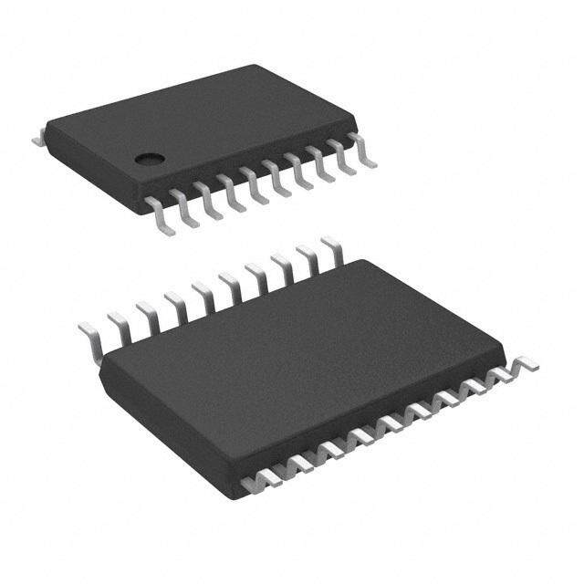
ADG3245 VOUT 3.3V SUPPLY 5 1.8V SEL = 0V G324 PCLAURGD- I(N1) CARD I/O CPU D HT A CU WITUTP 45 SO RAM 2 G3 PCLAURGD- I(N2) CARD I/O 0V SWITCH 3.3V VIN AD INPUT Figure 10.3.3 V to 1.8 V Voltage Translation, SEL = 0 V Bus Isolation Figure 12.ADG3245 in a Hot Plug Application A common requirement of bus architectures is low capacitance There are many systems that require the ability to handle hot loading of the bus. Such systems require bus bridge devices that swapping, such as docking stations, PCI boards for servers, and extend the number of loads on the bus without exceeding the line cards for telecommunications switches. If the bus can be specifications. Because the ADG3245 is designed specifically for isolated prior to insertion or removal, then there is more control applications that do not need drive yet require simple logic over the hot swap event. This isolation can be achieved using a functions, it solves this requirement. The device isolates access bus switch. The bus switches are positioned on the hot swap card to the bus, thus minimizing capacitance loading. between the connector and the devices. During hot swap, the ground pin of the hot swap card must connect to the ground pin LOAD A LOAD C of the back plane before any other signal or power pins. Analog Switching BUS/ BACKPLANE Bus switches can be used in many analog switching applications; for example, video graphics. Bus switches can have lower on BUS SWITCH LOAD B LOAD D resistance, smaller ON and OFF channel capacitance and thus LOCATION improved frequency performance than their analog counterparts. Figure 11.Location of Bus Switched in a Bus The bus switch channel itself consisting solely of an NMOS Isolation Application switch limits the operating voltage (see TPC1 for a typical Hot Plug and Hot Swap Isolation plot), but in many cases, this does not present an issue. The ADG3245 is suitable for hot swap and hot plug applications. High Impedance During Power-Up/Power-Down The output signal of the ADG3245 is limited to a voltage that is To ensure the high impedance state during power-up or power- below the VCC supply, as shown in Figures 6, 8, and 10. Therefore down, BE should be tied to VCC through a pull-up resistor; the the switch acts like a buffer to take the impact from hot insertion, minimum value of the resistor is determined by the current- protecting vital and expensive chipsets from damage. sinking capability of the driver. In hot-plug applications, the system cannot be shutdown when new hardware is being added. To overcome this, a bus switch can PACKAGE AND PINOUT be positioned on the backplane between the bus devices and the The ADG3245 is packaged in both a small 20-lead TSSOP or a hot plug connectors. The bus switch is turned off during hot plug. tiny 20-lead LFCSP package. The area of the TSSOP option is Figure 12 shows a typical example of this type of application. 37.5 mm2, while the area of the LFCSP option is 16 mm2. This leads to a 57% savings in board space when using the LFCSP pack- age compared with the TSSOP package. This makes the LFCSP option an excellent choice for space-constrained applications. The ADG3245 in the TSSOP package offers a flowthrough pinout. The term flowthrough signifies that all the inputs are on opposite sides from the outputs. A flowthrough pinout simplifies the PCB layout. –10– REV.(cid:36)
ADG3245 OUTLINE DIMENSIONS 4.10 0.30 4.00SQ 0.25 PIN1 3.90 0.18 INDICATOR PIN1 0.50 16 20 INDICATOR BSC 15 1 EXPOSED 2.30 PAD 2.10SQ 2.00 11 5 0.65 10 6 0.20MIN TOPVIEW 0.60 BOTTOMVIEW 0.55 0.80 FORPROPERCONNECTIONOF 0.75 THEEXPOSEDPAD,REFERTO 0.05MAX THEPINCONFIGURATIONAND 0.70 0.02NOM FUNCTIONDESCRIPTIONS SECTIONOFTHISDATASHEET. COPLANARITY SEATING 0.08 PLANE COMPLIANTTOJED0E.2C0SRTEAFNDARDSMO-220-WGGD-1. 08-16-2010-B Figure 12. 20-Lead Lead Frame Chip Scale Package [LFCSP_WQ] 4 mm × 4 mm Body, Very Very Thin Quad (CP-20-6) Dimensions shown in millimeters 6.60 6.50 6.40 20 11 4.50 4.40 4.30 6.40 BSC 1 10 PIN 1 0.65 BSC 0.15 1.20 MAX 0.20 0.05 0.09 0.75 0.30 8° 0.60 COPLANARITY 0.19 SEATING 0° 0.45 0.10 PLANE COMPLIANT TO JEDEC STANDARDS MO-153-AC Figure 13. 20-Lead Thin Shrink Small Outline Package [TSSOP] (RU-20) Dimensions shown in millimeters REV. C –11–
ADG3245 ORDERING GUIDE Model1 Temperature Range Package Description Package Option ADG3245BCPZ −40°C to +85°C 20-Lead Lead Frame Chip Scale Package [LFCSP_WQ] CP-20-6 ADG3245BRU −40°C to +85°C 20-Lead Thin Shrink Small Outline Package [TSSOP] RU-20 ADG3245BRU-REEL7 −40°C to +85°C 20-Lead Thin Shrink Small Outline Package [TSSOP] RU-20 ADG3245BRUZ −40°C to +85°C 20-Lead Thin Shrink Small Outline Package [TSSOP] RU-20 ADG3245BRUZ-REEL7 −40°C to +85°C 20-Lead Thin Shrink Small Outline Package [TSSOP] RU-20 1 Z = RoHS Compliant Part. REVISION HISTORY 12/15—Rev. B to Rev. C Change to Mixed Voltage Operation, Level Translation Section ................................................................................................ 9 4/13—Rev. A to Rev. B Change to LFCSP Package Figure ................................................. 3 Change to Ordering Guide ............................................................ 12 10/12—Rev. 0 to Rev. A Added EPAD Note ............................................................................ 3 Updated Outline Dimensions ...................................................... 11 Changes to Ordering Guide .......................................................... 12 5/03—Revision 0—Initial Version ©2003–2015 Analog Devices, Inc. All rights reserved. Trademarks and registered trademarks are the property of their respective owners. D03011-0-12/15(C) –12– REV. C