ICGOO在线商城 > 集成电路(IC) > 接口 - 模拟开关,多路复用器,多路分解器 > ADG1608BCPZ-REEL7
 Datasheet下载
- 型号: ADG1608BCPZ-REEL7
- 制造商: Analog
- 库位|库存: xxxx|xxxx
- 要求:
| 数量阶梯 | 香港交货 | 国内含税 |
| +xxxx | $xxxx | ¥xxxx |
查看当月历史价格
查看今年历史价格
ADG1608BCPZ-REEL7产品简介:
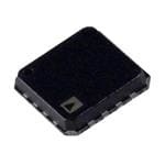
ICGOO电子元器件商城为您提供ADG1608BCPZ-REEL7由Analog设计生产,在icgoo商城现货销售,并且可以通过原厂、代理商等渠道进行代购。 ADG1608BCPZ-REEL7价格参考。AnalogADG1608BCPZ-REEL7封装/规格:接口 - 模拟开关,多路复用器,多路分解器, 1 Circuit IC Switch 8:1 4.5Ohm 16-LFCSP-WQ (3x3)。您可以下载ADG1608BCPZ-REEL7参考资料、Datasheet数据手册功能说明书,资料中有ADG1608BCPZ-REEL7 详细功能的应用电路图电压和使用方法及教程。
ADG1608BCPZ-REEL7是Analog Devices Inc.推出的一款模拟开关/多路复用器,广泛应用于需要高精度信号切换的电子系统中。其典型应用场景包括便携式医疗设备(如血糖仪、心电图机)、工业测量仪器、数据采集系统和自动化测试设备。该器件支持8通道单刀单掷(SPST)开关功能,可实现模拟或数字信号的灵活路由,在电池供电设备中表现出低功耗和高效率的优势。

由于具备宽电源电压范围(±5V至±20V)、低导通电阻和快速开关速度,ADG1608BCPZ-REEL7适用于处理微弱模拟信号的精密系统,例如传感器信号调理电路或多通道模数转换器(ADC)前端切换。其CMOS工艺确保了低漏电流和高隔离度,适合高阻抗信号源的应用环境。

此外,该器件采用TSSOP封装,体积小巧,适合空间受限的消费类电子产品和通信设备中的信号管理。在音频与视频信号切换、自动增益控制电路以及多路传感器接口中也有广泛应用。整体而言,ADG1608BCPZ-REEL7凭借高可靠性、优异的动态性能和稳定的温度特性,成为工业、医疗及通用电子系统中多路信号切换的理想选择。
| 参数 | 数值 |
| 产品目录 | 集成电路 (IC) |
| 描述 | IC MULTIPLEXER 8X1 16LFCSP |
| 产品分类 | |
| 品牌 | Analog Devices Inc |
| 数据手册 | |
| 产品图片 |
|
| 产品型号 | ADG1608BCPZ-REEL7 |
| rohs | 无铅 / 符合限制有害物质指令(RoHS)规范要求 |
| 产品系列 | - |
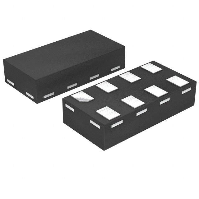
| 供应商器件封装 | 16-LFCSP-WQ(3x3) |
| 其它名称 | ADG1608BCPZ-REEL7TR |
| 功能 | 多路复用器 |
| 包装 | 带卷 (TR) |
| 安装类型 | 表面贴装 |
| 导通电阻 | 4.5 欧姆 |
| 封装/外壳 | 16-WFQFN 裸露焊盘,CSP |
| 工作温度 | -40°C ~ 125°C |
| 标准包装 | 1,500 |
| 电压-电源,单/双 (±) | 3.3 V ~ 16 V, ±1.65 V ~ 4 V |
| 电压源 | 单/双电源 |
| 电流-电源 | 300µA |
| 电路 | 1 x 8:1 |


- 商务部:美国ITC正式对集成电路等产品启动337调查
- 曝三星4nm工艺存在良率问题 高通将骁龙8 Gen1或转产台积电
- 太阳诱电将投资9.5亿元在常州建新厂生产MLCC 预计2023年完工
- 英特尔发布欧洲新工厂建设计划 深化IDM 2.0 战略
- 台积电先进制程称霸业界 有大客户加持明年业绩稳了
- 达到5530亿美元!SIA预计今年全球半导体销售额将创下新高
- 英特尔拟将自动驾驶子公司Mobileye上市 估值或超500亿美元
- 三星加码芯片和SET,合并消费电子和移动部门,撤换高东真等 CEO
- 三星电子宣布重大人事变动 还合并消费电子和移动部门
- 海关总署:前11个月进口集成电路产品价值2.52万亿元 增长14.8%


PDF Datasheet 数据手册内容提取
4.5 Ω R , 4-/8-Channel ON ±5 V, +12 V, +5 V, and +3.3 V Multiplexers Data Sheet ADG1608/ADG1609 FEATURES FUNCTIONAL BLOCK DIAGRAMS 4.5 Ω typical on resistance 1 Ω on-resistance flatness ADG1608 Up to 470 mA continuous current S1 ±3.3 V to ±8 V dual-supply operation 3.3 V to 16 V single-supply operation D No V supply required L 3 V logic-compatible inputs S8 Rail-to-rail operation 16-lead TSSOP and 16-lead, 3 mm × 3 mm LFCSP 1-OF-8 DECODER APPLICATIONS A0 A1 A2 EN 08318-001 Communication systems Figure 1. Medical systems Audio signal routing ADG1609 Video signal routing Automatic test equipment S1A DA Data acquisition systems S4A Battery-powered systems S1B Sample-and-hold systems DB Relay replacements S4B 1-OF-4 DECODER A0 A1 EN 08318-002 Figure 2. GENERAL DESCRIPTION The ADG1608/ADG1609 are monolithic CMOS analog multip- The low on resistance of these switches make them ideal solu- lexers comprising eight single channels and four differential tions for data acquisition and gain switching applications where channels, respectively. The ADG1608 switches one of eight low on resistance and distortion is critical. The on-resistance inputs to a common output, as determined by the 3-bit binary profile is very flat over the full analog input range, ensuring address lines, A0, A1, and A2. The ADG1609 switches one of excellent linearity and low distortion when switching audio four differential inputs to a common differential output, as signals. determined by the 2-bit binary address lines, A0 and A1. An CMOS construction ensures ultralow power dissipation, making EN input on both devices is used to enable or disable the device. the parts ideally suited for portable and battery-powered When disabled, all channels are switched off. instruments. Each switch conducts equally well in both directions when on PRODUCT HIGHLIGHTS and has an input signal range that extends to the supplies. In the 1. 8 Ω maximum on resistance over temperature. off condition, signal levels up to the supplies are blocked. All switches exhibit break-before-make switching action. Inherent 2. Minimum distortion: THD + N = 0.04% in the design is low charge injection for minimum transients 3. 3 V logic-compatible digital inputs: VINH = 2.0 V, VINL = 0.8 V. when switching the digital inputs. 4. No VL logic power supply required. 5. Ultralow power dissipation: <8 nW. 6. 16-lead TSSOP and 16-lead, 3 mm × 3 mm LFCSP. Rev. A Document Feedback Information furnished by Analog Devices is believed to be accurate and reliable. However, no responsibility is assumed by Analog Devices for its use, nor for any infringements of patents or other One Technology Way, P.O. Box 9106, Norwood, MA 02062-9106, U.S.A. rights of third parties that may result from its use. Specifications subject to change without notice. No license is granted by implication or otherwise under any patent or patent rights of Analog Devices. Tel: 781.329.4700 ©2009–2015 Analog Devices, Inc. All rights reserved. Trademarks and registered trademarks are the property of their respective owners. Technical Support www.analog.com
ADG1608/ADG1609 Data Sheet TABLE OF CONTENTS Features .............................................................................................. 1 Continuous Current per Channel, S or D ..................................7 Applications ....................................................................................... 1 Absolute Maximum Ratings ............................................................8 Functional Block Diagrams ............................................................. 1 ESD Caution...................................................................................8 General Description ......................................................................... 1 Pin Configurations and Function Descriptions ............................9 Product Highlights ........................................................................... 1 Typical Performance Characteristics ........................................... 11 Revision History ............................................................................... 2 Test Circuits ..................................................................................... 14 Specifications ..................................................................................... 3 Terminology .................................................................................... 17 ±5 V Dual Supply ......................................................................... 3 Outline Dimensions ....................................................................... 18 12 V Single Supply ........................................................................ 4 Ordering Guide .......................................................................... 18 5 V Single Supply .......................................................................... 5 3.3 V Single Supply ....................................................................... 6 REVISION HISTORY 9/15—Rev. 0 to Rev. A Change to Table 7 ............................................................................. 8 Updated Outline Dimensions ....................................................... 18 7/09—Revision 0: Initial Version Rev. A | Page 2 of 20
Data Sheet ADG1608/ADG1609 SPECIFICATIONS ±5 V DUAL SUPPLY V = +5 V ± 10%, V = −5 V ± 10%, GND = 0 V, unless otherwise noted. DD SS Table 1. −40°C to −40°C to Parameter 25°C +85°C +125°C Unit Test Conditions/Comments ANALOG SWITCH Analog Signal Range VDD to VSS V On Resistance (RON) 4.5 Ω typ VS = ±4.5 V, IS = −10 mA; see Figure 25 5 7 8 Ω max VDD = ±4.5 V, VSS = ±4.5 V On-Resistance Match Between Channels (∆RON) 0.12 Ω typ VS = ±4.5 V, IS = −10 mA 0.25 0.3 0.35 Ω max On-Resistance Flatness (RFLAT(ON)) 1 Ω typ VS = ±4.5 V, IS = −10 mA 1.3 1.7 2 Ω max LEAKAGE CURRENTS VDD = +5.5 V, VSS = −5.5 V Source Off Leakage, IS (Off) ±0.02 nA typ VS = ±4.5 V, VD = ∓4.5 V; see Figure 26 ±0.1 ±0.5 ±3 nA max Drain Off Leakage, ID (Off) ±0.03 nA typ VS = ±4.5 V, VD = ∓4.5 V; see Figure 26 ADG1608 ±0.15 ±2 ±14 nA max ADG1609 ±0.15 ±1 ±7 nA max Channel On Leakage, ID, IS (On) ±0.03 nA typ VS = VD = ±4.5 V; see Figure 27 ±0.15 ±2 ±14 nA max DIGITAL INPUTS Input High Voltage, VINH 2.0 V min Input Low Voltage, VINL 0.8 V max Input Current, IINL or IINH ±1 nA typ VIN = VGND or VDD ±0.1 µA max Digital Input Capacitance, CIN 4 pF typ DYNAMIC CHARACTERISTICS1 Transition Time, tTRANSITION 150 ns typ RL = 300 Ω, CL = 35 pF 182 230 258 ns max VS = 2.5 V; see Figure 28 tON (EN) 106 ns typ RL = 300 Ω, CL = 35 pF 132 150 160 ns max VS = 2.5 V; see Figure 30 tOFF (EN) 113 ns typ RL = 300 Ω, CL = 35 pF 144 178 202 ns max VS = 2.5 V; see Figure 30 Break-Before-Make Time Delay, tD 47 ns typ RL = 300 Ω, CL = 35 pF 30 ns min VS1 = VS2 = 2.5 V; see Figure 29 Charge Injection 24 pC typ VS = 0 V, RS = 0 Ω, CL = 1 nF; see Figure 31 Off Isolation −64 dB typ RL = 50 Ω, CL = 5 pF, f = 1 MHz; see Figure 32 Channel-to-Channel Crosstalk −64 dB typ RL = 50 Ω, CL = 5 pF, f = 1 MHz; see Figure 34 Total Harmonic Distortion + Noise (THD + N) 0.04 % typ RL = 110 Ω, VS = 5 V p-p, f = 20 Hz to 20 kHz; see Figure 35 −3 dB Bandwidth RL = 50 Ω, CL = 5 pF; see Figure 33 ADG1608 40 MHz typ ADG1609 71 MHz typ CS (Off) 20 pF typ VS = 0 V, f = 1 MHz CD (Off) ADG1608 120 pF typ VS = 0 V, f = 1 MHz ADG1609 61 pF typ VS = 0 V, f = 1 MHz CD, CS (On) ADG1608 153 pF typ VS = 0 V, f = 1 MHz ADG1609 85 pF typ VS = 0 V, f = 1 MHz POWER REQUIREMENTS VDD = +5.5 V, VSS = −5.5 V IDD 0.001 µA typ Digital inputs = 0 V or VDD 1.0 µA max VDD/VSS ±3.3/±8 V min/max 1 Guaranteed by design, but not subject to production test. Rev. A | Page 3 of 20
ADG1608/ADG1609 Data Sheet 12 V SINGLE SUPPLY V = 12 V ± 10%, V = 0 V, GND = 0 V, unless otherwise noted. DD SS Table 2. −40°C to −40°C to Parameter 25°C +85°C +125°C Unit Test Conditions/Comments ANALOG SWITCH Analog Signal Range 0 V to VDD V On Resistance (RON) 4 Ω typ VS = 0 V to 10 V, IS = −10 mA; see Figure 25 4.5 6.5 7.5 Ω max VDD = 10.8 V, VSS = 0 V On-Resistance Match Between Channels (∆RON) 0.12 Ω typ VS = 10 V, IS = −10 mA 0.25 0.3 0.35 Ω max On-Resistance Flatness (RFLAT(ON)) 0.9 Ω typ VS = 0 V to 10 V, IS = −10 mA 1.2 1.6 1.9 Ω max LEAKAGE CURRENTS VDD = 13.2 V, VSS = 0 V Source Off Leakage, IS (Off) ±0.02 nA typ VS = 1 V/10 V, VD = 10 V/1 V; see Figure 26 ±0.1 ±0.5 ±3 nA max Drain Off Leakage, ID (Off) ±0.03 nA typ VS = 1 V/10 V, VD = 10 V/1 V; see Figure 26 ADG1608 ±0.15 ±2 ±14 nA max ADG1609 ±0.15 ±1 ±7 nA max Channel On Leakage, ID, IS (On) ±0.03 nA typ VS = VD = 1 V or 10 V; see Figure 27 ±0.15 ±2 ±14 nA max DIGITAL INPUTS Input High Voltage, VINH 2.0 V min Input Low Voltage, VINL 0.8 V max Input Current, IINL or IINH ±1 nA typ VIN = VGND or VDD ±0.1 µA max Digital Input Capacitance, CIN 4 pF typ DYNAMIC CHARACTERISTICS1 Transition Time, tTRANSITION 113 ns typ RL = 300 Ω, CL = 35 pF 141 172 196 ns max VS = 8 V; see Figure 28 tON (EN) 80 ns typ RL = 300 Ω, CL = 35 pF 94 101 110 ns max VS = 8 V; see Figure 30 tOFF (EN) 77 ns typ RL = 300 Ω, CL = 35 pF 93 117 140 ns max VS = 8 V; see Figure 30 Break-Before-Make Time Delay, tD 47 ns typ RL = 300 Ω, CL = 35 pF 30 ns min VS1 = VS2 = 8 V; see Figure 29 Charge Injection 29 pC typ VS = 6 V, RS = 0 Ω, CL = 1 nF; see Figure 31 Off Isolation −64 dB typ RL = 50 Ω, CL = 5 pF, f = 1 MHz; see Figure 32 Channel-to-Channel Crosstalk −64 dB typ RL = 50 Ω, CL = 5 pF, f = 1 MHz; see Figure 34 Total Harmonic Distortion + Noise (THD + N) 0.04 % typ RL = 110 Ω, VS = 5 V p-p, f = 20 Hz to 20 kHz; see Figure 35 −3 dB Bandwidth RL = 50 Ω, CL = 5 pF; see Figure 33 ADG1608 40 MHz typ ADG1609 78 MHz typ CS (Off) 19 pF typ VS = 6 V, f = 1 MHz CD (Off) ADG1608 117 pF typ VS = 6 V, f = 1 MHz ADG1609 59 pF typ VS = 6 V, f = 1 MHz CD, CS (On) ADG1608 149 pF typ VS = 6 V, f = 1 MHz ADG1609 84 pF typ VS = 6 V, f = 1 MHz POWER REQUIREMENTS VDD = 12 V IDD 0.001 µA typ Digital inputs = 0 V or VDD 1.0 µA max ADG1608 300 µA typ Digital inputs = 5 V 480 µA max ADG1609 225 µA typ Digital inputs = 5 V 360 µA max VDD 3.3/16 V min/max 1 Guaranteed by design, but not subject to production test. Rev. A | Page 4 of 20
Data Sheet ADG1608/ADG1609 5 V SINGLE SUPPLY V = 5 V ± 10%, V = 0 V, GND = 0 V, unless otherwise noted. DD SS Table 3. −40°Cto −40°C to Parameter 25°C +85°C +125°C Unit Test Conditions/Comments ANALOG SWITCH Analog Signal Range 0 V to VDD V On Resistance (RON) 8.5 Ω typ VS = 0 V to 4.5 V, IS = −10 mA; see Figure 25 10 12.5 14 Ω max VDD = 4.5 V, VSS = 0 V On-Resistance Match Between Channels (∆RON) 0.15 Ω typ VS = 0 V to 4.5 V, IS = −10 mA 0.3 0.35 0.4 Ω max On-Resistance Flatness (RFLAT(ON)) 1.7 Ω typ VS = 0 V to 4.5 V, IS = −10 mA 2.3 2.7 3 Ω max LEAKAGE CURRENTS VDD = 5.5 V, VSS = 0 V Source Off Leakage, IS (Off) ±0.01 nA typ VS = 1 V/4.5 V, VD = 4.5 V/1 V; see Figure 26 ±0.1 ±0.5 ±3 nA max Drain Off Leakage, ID (Off) ±0.01 nA typ VS = 1 V/4.5 V, VD = 4.5 V/1 V; see Figure 26 ADG1608 ±0.15 ±2 ±14 nA max ADG1609 ±0.15 ±1 ±7 nA max Channel On Leakage, ID, IS (On) ±0.01 nA typ VS = VD = 1 V or 4.5 V; see Figure 27 ±0.15 ±2 ±14 nA max DIGITAL INPUTS Input High Voltage, VINH 2.0 V min Input Low Voltage, VINL 0.8 V max Input Current, IINL or IINH ±1 nA typ VIN = VGND or VDD ±0.1 µA max Digital Input Capacitance, CIN 4 pF typ DYNAMIC CHARACTERISTICS1 Transition Time, tTRANSITION 193 ns typ RL = 300 Ω, CL = 35 pF 251 301 339 ns max VS = 2.5 V; see Figure 28 tON (EN) 115 ns typ RL = 300 Ω, CL = 35 pF 152 171 184 ns max VS = 2.5 V; see Figure 30 tOFF (EN) 140 ns typ RL = 300 Ω, CL = 35 pF 184 225 259 ns max VS = 2.5 V; see Figure 30 Break-Before-Make Time Delay, tD 66 ns typ RL = 300 Ω, CL = 35 pF 37 ns min VS1 = VS2 = 2.5 V; see Figure 29 Charge Injection 11 pC typ VS = 2.5 V, RS = 0 Ω, CL = 1 nF; see Figure 31 Off Isolation −64 dB typ RL = 50 Ω, CL = 5 pF, f = 100 kHz; see Figure 32 Channel-to-Channel Crosstalk −64 dB typ RL = 50 Ω, CL = 5 pF, f = 100 kHz; see Figure 34 Total Harmonic Distortion + Noise (THD + N) 0.3 % typ RL = 110 Ω, f = 20 Hz to 20 kHz, VS = 3.5 V p-p; see Figure 35 −3 dB Bandwidth RL = 50 Ω, CL = 5 pF; see Figure 33 ADG1608 37 MHz typ ADG1609 72 MHz typ CS (Off) 22 pF typ VS = 2.5 V, f = 1 MHz CD (Off) VS = 2.5 V, f = 1 MHz ADG1608 136 pF typ ADG1609 68 pF typ CD, CS (On) VS = 2.5 V, f = 1 MHz ADG1608 168 pF typ ADG1609 94 pF typ POWER REQUIREMENTS VDD = 5.5 V IDD 0.001 µA typ Digital inputs = 0 V or VDD 1.0 µA max VDD 3.3/16 V min/max 1 Guaranteed by design, but not subject to production test. Rev. A | Page 5 of 20
ADG1608/ADG1609 Data Sheet 3.3 V SINGLE SUPPLY V = 3.3 V, V = 0 V, GND = 0 V, unless otherwise noted. DD SS Table 4. −40°C to −40°C to Parameter 25°C +85°C +125°C Unit Test Conditions/Comments ANALOG SWITCH Analog Signal Range 0 V to VDD V On Resistance (RON) 13.5 15 16.5 Ω typ VS = 0 V to VDD, IS = −10 mA; see Figure 25, VDD = 3.3 V, VSS = 0 V On-Resistance Match Between Channels (∆RON) 0.25 0.28 0.3 Ω typ VS = 0 V to VDD, IS = −10 mA On-Resistance Flatness (RFLAT(ON)) 5 5.5 6.5 Ω typ VS = 0 V to VDD, IS = −10 mA LEAKAGE CURRENTS VDD = 3.6 V, VSS = 0 V Source Off Leakage, IS (Off) ±0.01 nA typ VS = 0.6 V/3 V, VD = 3 V/0.6 V; see Figure 26 ±0.1 ±0.5 ±3 nA max Drain Off Leakage, ID (Off) ±0.01 nA typ VS = 0.6 V/3 V, VD = 3 V/0.6 V; see Figure 26 ADG1608 ±0.15 ±2 ±14 nA max ADG1609 ±0.15 ±1 ±7 nA max Channel On Leakage, ID, IS (On) ±0.01 nA typ VS = VD = 0.6 V or 3 V; see Figure 27 ±0.15 ±2 ±14 nA max DIGITAL INPUTS Input High Voltage, VINH 2.0 V min Input Low Voltage, VINL 0.8 V max Input Current, IINL or IINH ±1 nA typ VIN = VGND or VDD ±0.1 µA max Digital Input Capacitance, CIN 4 pF typ DYNAMIC CHARACTERISTICS1 Transition Time, tTRANSITION 312 ns typ RL = 300 Ω, CL = 35 pF 437 498 542 ns max VS = 1.5 V; see Figure 28 tON (EN) 216 ns typ RL = 300 Ω, CL = 35 pF 309 331 344 ns max VS = 1.5 V; see Figure 30 tOFF (EN) 236 ns typ RL = 300 Ω, CL = 35 pF 316 367 411 ns max VS = 1.5 V; see Figure 30 Break-Before-Make Time Delay, tD 104 ns typ RL = 300 Ω, CL = 35 pF 48 ns min VS1 = VS2 = 1.5 V; see Figure 29 Charge Injection 6 pC typ VS = 1.5 V, RS = 0 Ω, CL = 1 nF; see Figure 31 Off Isolation −64 dB typ RL = 50 Ω, CL = 5 pF, f = 100 kHz; see Figure 32 Channel-to-Channel Crosstalk −64 dB typ RL = 50 Ω, CL = 5 pF, f = 100 kHz; see Figure 34 Total Harmonic Distortion + Noise (THD + N) 0.5 % typ RL = 110 Ω, f = 20 Hz to 20 kHz, VS = 2 V p-p; see Figure 35 −3 dB Bandwidth RL = 50 Ω, CL = 5 pF; see Figure 33 ADG1608 34 MHz typ ADG1609 72 MHz typ CS (Off) 23 pF typ VS = 1.5 V, f = 1 MHz CD (Off) VS = 1.5 V, f = 1 MHz ADG1608 145 pF typ ADG1609 72 pF typ CD, CS (On) VS = 1.5 V, f = 1 MHz ADG1608 173 pF typ ADG1609 95 pF typ POWER REQUIREMENTS VDD = 3.6 V IDD 0.001 µA typ Digital inputs = 0 V or VDD 1.0 µA max VDD 3.3/16 V min/max 1 Guaranteed by design, but not subject to production test. Rev. A | Page 6 of 20
Data Sheet ADG1608/ADG1609 CONTINUOUS CURRENT PER CHANNEL, S OR D Table 5. ADG1608 Parameter 25°C 85°C 125°C Unit CONTINUOUS CURRENT, S OR D V = +5 V, V = −5 V DD SS TSSOP (θ = 112.6°C/W) 290 180 100 mA max JA LFCSP (θ = 48.7°C/W) 470 255 120 mA max JA V = 12 V, V = 0 V DD SS TSSOP (θ = 112.6°C/W) 213 129 73 mA max JA LFCSP (θ = 48.7°C/W) 346 185 84 mA max JA V = 5 V, V = 0 V DD SS TSSOP (θ = 112.6°C/W) 157 101 63 mA max JA LFCSP (θ = 48.7°C/W) 252 150 77 mA max JA V = 3.3 V, V = 0 V DD SS TSSOP (θ = 112.6°C/W) 126 87 56 mA max JA LFCSP (θ = 48.7°C/W) 206 129 73.5 mA max JA Table 6. ADG1609 Parameter 25°C 85°C 125°C Unit CONTINUOUS CURRENT, S OR D V = +5 V, V = −5 V DD SS TSSOP (θ = 112.6°C/W) 147 98 63 mA max JA LFCSP (θ = 48.7°C/W) 245 147 77 mA max JA V = 12 V, V = 0 V DD SS TSSOP (θ = 112.6°C/W) 157 101 63 mA max JA LFCSP (θ = 48.7°C/W) 255 150 77 mA max JA V = 5 V, V = 0 V DD SS TSSOP (θ = 112.6°C/W) 115 80 52 mA max JA LFCSP (θ = 48.7°C/W) 189 119 70 mA max JA V = 3.3 V, V = 0 V DD SS TSSOP (θ = 112.6°C/W) 94 66 45 mA max JA LFCSP (θ = 48.7°C/W) 154 101 63 mA max JA Rev. A | Page 7 of 20
ADG1608/ADG1609 Data Sheet ABSOLUTE MAXIMUM RATINGS T = 25°C, unless otherwise noted. A Stresses at or above those listed under Absolute Maximum Ratings may cause permanent damage to the product. This is a Table 7. stress rating only; functional operation of the product at these Parameter Rating or any other conditions above those indicated in the operational V to V 18 V DD SS section of this specification is not implied. Operation beyond V to GND −0.3 V to +18 V DD the maximum operating conditions for extended periods may V to GND +0.3 V to −18 V SS affect product reliability. Analog Inputs1 V − 0.3 V to V + 0.3 V or SS DD 30 mA, whichever occurs first ESD CAUTION Digital Inputs1 GND − 0.3 V to V + 0.3 V or DD 30 mA, whichever occurs first Peak Current, S or D 710 mA (pulsed at 1 ms, 10% duty cycle maximum) Continuous Current, S or D2 Data + 15% Operating Temperature Range Industrial −40°C to +125°C Storage Temperature Range −65°C to +150°C Junction Temperature 150°C 16-Lead TSSOP, θJA Thermal 112.6°C/W Impedance, 0 Airflow (4-Layer Board) 16-Lead LFCSP, θJA Thermal 48.7°C/W Impedance, 0 Airflow (4-Layer Board) Reflow Soldering Peak 260°C Temperature, Pb-free 1 Overvoltages at IN, S, or D are clamped by internal diodes. Current should be limited to the maximum ratings given. 2 See Table 5 and Table 6. Rev. A | Page 8 of 20
Data Sheet ADG1608/ADG1609 PIN CONFIGURATIONS AND FUNCTION DESCRIPTIONS N 0 1 2 E A A A 6 5 4 3 1 1 1 1 PIN 1 VSS 1 INDICATOR 12GND S1 2 ADG1608 11VDD A0 1 16 A1 S2 3 TOP VIEW 10S5 S3 4 (Not to Scale) 9 S6 EN 2 15 A2 VSS 3 14 GND 5 6 7 8 S1 4 ADG1608 13 VDD 4S D 8S 7S TOP VIEW S2 5 (Not to Scale) 12 S5 NOTES 1. THE EXPOSED PAD IS CONNECTED S3 6 11 S6 INTERNALLY. FOR INCREASED RELIABILITY OF THE SOLDER S4 7 10 S7 JOINTS AND MAXIMUM THERMAL D 8 9 S8 08318-003 CTTHHAAEP TAS BTUIHBLESIT TPYRA, AIDTT BEISE, V RSSEOSC.LODMERMEEDN DTEOD 08318-004 Figure 3. ADG1608 Pin Configuration (TSSOP) Figure 4. ADG1608 Pin Configuration (LFCSP) Table 8. ADG1608 Pin Function Descriptions Pin No. TSSOP LFCSP Mnemonic Description 1 15 A0 Logic Control Input. 2 16 EN Active High Digital Input. When this pin is low, the device is disabled and all switches are off. When this pin is high, Ax logic inputs determine on switches. 3 1 V Most Negative Power Supply Potential. In single-supply applications, this pin can be connected to ground. SS 4 2 S1 Source Terminal 1. Can be an input or an output. 5 3 S2 Source Terminal 2. Can be an input or an output. 6 4 S3 Source Terminal 3. Can be an input or an output. 7 5 S4 Source Terminal 4. Can be an input or an output. 8 6 D Drain Terminal. Can be an input or an output. 9 7 S8 Source Terminal 8. Can be an input or an output. 10 8 S7 Source Terminal 7. Can be an input or an output. 11 9 S6 Source Terminal 6. Can be an input or an output. 12 10 S5 Source Terminal 5. Can be an input or an output. 13 11 V Most Positive Power Supply Potential. DD 14 12 GND Ground (0 V) Reference. 15 13 A2 Logic Control Input. 16 14 A1 Logic Control Input. N/A EP EP Exposed Pad. The exposed pad is connected internally. For increased reliability of the solder joints and maximum thermal capability, it is recommended that the pad be soldered to the substrate, V . SS Table 9. ADG1608 Truth Table A2 A1 A0 EN On Switch X1 X1 X1 0 None 0 0 0 1 1 0 0 1 1 2 0 1 0 1 3 0 1 1 1 4 1 0 0 1 5 1 0 1 1 6 1 1 0 1 7 1 1 1 1 8 1 X = don’t care. Rev. A | Page 9 of 20
ADG1608/ADG1609 Data Sheet D NE 0A 1A NG 6 5 4 3 1 1 1 1 PIN 1 VSS 1 INDICATOR 12VDD S1A 2 11S1B ADG1609 S2A 3 TOP VIEW 10S2B A0 1 16 A1 S3A 4 (Not to Scale) 9 S3B EN 2 15 GND VSS 3 14 VDD 5 6 7 8 S1A 4 ADG1609 13 S1B A4 AD BS B4 TOP VIEW S S S2A 5 (Not to Scale) 12 S2B NOTES 1. THE EXPOSED PAD IS CONNECTED S3A 6 11 S3B INTERNALLY. FOR INCREASED RELIABILITY OF THE SOLDER S4A 7 10 S4B JOINTS AND MAXIMUM THERMAL DA 8 9 DB 08318-005 TCTHHAEAP TAS BTUIHBLESIT TPYRA, AIDTT BEISE, V RSSEOSC.LODMERMEEDN DTEOD 08318-006 Figure 5. ADG1609 Pin Configuration (TSSOP) Figure 6. ADG1609 Pin Configuration (LFCSP) Table 10. ADG1609 Pin Function Descriptions Pin No. TSSOP LFCSP Mnemonic Description 1 15 A0 Logic Control Input. 2 16 EN Active High Digital Input. When this pin is low, the device is disabled and all switches are off. When this pin is high, Ax logic inputs determine on switches. 3 1 V Most Negative Power Supply Potential. In single-supply applications, this pin can be connected to ground. SS 4 2 S1A Source Terminal 1A. Can be an input or an output. 5 3 S2A Source Terminal 2A. Can be an input or an output. 6 4 S3A Source Terminal 3A. Can be an input or an output. 7 5 S4A Source Terminal 4A. Can be an input or an output. 8 6 DA Drain Terminal A. Can be an input or an output. 9 7 DB Drain Terminal B. Can be an input or an output. 10 8 S4B Source Terminal 4B. Can be an input or an output. 11 9 S3B Source Terminal 3B. Can be an input or an output. 12 10 S2B Source Terminal 2B. Can be an input or an output. 13 11 S1B Source Terminal 1B. Can be an input or an output. 14 12 V Most Positive Power Supply Potential. DD 15 13 GND Ground (0 V) Reference. 16 14 A1 Logic Control Input. N/A EP EP Exposed Pad. The exposed pad is connected internally. For increased reliability of the solder joints and maximum thermal capability, it is recommended that the pad be soldered to the substrate, V . SS Table 11. ADG1609 Truth Table A1 A0 EN On Switch Pair X1 X1 0 None 0 0 1 1 0 1 1 2 1 0 1 3 1 1 1 4 1 X = don’t care. Rev. A | Page 10 of 20
Data Sheet ADG1608/ADG1609 TYPICAL PERFORMANCE CHARACTERISTICS 7 7 TA = 25°C VDD = 12V VSS = 0V 6 6 5 5 Ω) Ω) ANCE ( 4 VVDSSD == –+33..33VV ANCE ( 4 TTAA == ++18255°°CC T T RESIS 3 VVDSSD == –+55VV RESIS 3 TA = +25°C ON 2 VDD = +8V ON 2 TA = –40°C VSS = –8V 1 1 0 0 –8 –6 S–O4URCE– 2OR DRA0IN VOL2TAGE (V4) 6 8 08318-029 0 2 SOUR4CE OR DRA6IN VOLTA8GE (V) 10 12 08318-032 Figure 7. On Resistance vs. VD (VS) for Dual Supply Figure 10. On Resistance vs. VD (VS) for Different Temperatures, 12 V Single Supply 16 12 TA = 25°C 14 VDD = 3.3V VSS = 0V 10 TA = +125°C 12 Ω) Ω) 8 TA = +85°C SISTANCE ( 108 VVDSSD == 05VV SISTANCE ( 6 TTAA == +–4205°°CC E E N R 6 N R 4 O O 4 VVDSSD == 01V2V VVDSSD == 01V6V 2 2 VDD = 5V VSS = 0V 0 0 0 2 S4OURCE6 OR DRA8IN VO1L0TAGE (1V2) 14 16 08318-030 0 0.5 1.0SO1U.R5CE 2O.0R DR2A.5IN V3O.0LTAG3E.5 (V)4.0 4.5 5.0 08318-033 Figure 8. On Resistance vs. VD (VS) for Single Supply Figure 11. On Resistance vs. VD (VS) for Different Temperatures, 5 V Single Supply 18 7 VDD = 3.3V VDD = +5V VSS = 0V VSS = –5V 16 6 14 STANCE (Ω) 45 TTTAAA === +++1825525°°CC°C SISTANCE (Ω) 11028 TTTTAAAA ==== +++–41820255°5°°CCC°C N RESI 3 TA = –40°C ON RE 6 O 2 4 1 2 0 0–5 –4 –3SOU–2RCE –O1R DRA0IN VO1LTAGE2 (V) 3 4 5 08318-031 0 0.5 SOU1R.0CE OR D1.R5AIN VO2L.T0AGE (V)2.5 3.0 08318-020 Figure 9. On Resistance vs. VD (VS) for Different Temperatures, Figure 12. On Resistance vs. VD (VS) for Different Temperatures, ±5 V Dual Supply 3.3 V Single Supply Rev. A | Page 11 of 20
ADG1608/ADG1609 Data Sheet 12 9 10 VVVDSBSDIA =S= –=+5 5+VV4.5V/–4.5V 8 VVVDSBSDIA =S= 0=3V .03.V6V/3V 8 7 LEAKAGE CURRENT (nA) ––246420 IDID,II DS,II SS IS(( (OO( OO(FFOFNFFNF))) )) +–+ –– ++ ––+ LEAKAGE CURRENT (nA) 513426 IIDD,II,II DD SSIISS (((( OOOO((OOFFFFNNFFFF)))))) +––++– +–++–– –6 ID (OFF) + – 0 –80 20 40TEMPER60ATURE (°8C0) 100 120 08318-035 –10 20 40TEMPER6A0TURE (°8C0) 100 120 08318-018 Figure 13. ADG1608 Leakage Currents vs. Temperature, Figure 16. ADG1608 Leakage Currents vs. Temperature, ±5 V Dual Supply 3.3 V Single Supply 15 600 VVVDSBSDIA =S= 0=1V 21VV/10V ITDAD =P 2E5R° CCHANNEL 10 500 IIDSSD == 0+V12V nA) ID, IS (ON) + + ENT ( 5 IIDS ((OOFFFF)) –+ +– 400 CURR (µA)D300 AKAGE 0 ID200 IIDSSD == –+55VV LE –5 ID, IS (ON) – – IIDSSD == 0+V5V IS (OFF) – + 100 IDD = +3.3V ID (OFF) + – ISS = 0V –10 0 0 20 40TEMPER6A0TURE (°8C0) 100 120 08318-034 0 2 4 6LOGIC (V8) 10 12 14 08318-019 Figure 14. ADG1608 Leakage Currents vs. Temperature, Figure 17. IDD vs. Logic Level 12 V Single Supply 10 30 VDD = 5V 9 VSS = 0V VBIAS = 1V/4.5V 8 25 VDD= +12V A) 7 C) VSS= 0V AGE CURRENT (n 5346 IIDD,I,I D SIISS (( OO((OOFFNNFF)))) +––+ +–+– GE INJECTION (p1250 VVDSSD== –+55VV LEAK 2 IIDS ((OOFFFF)) –+ +– CHAR10 VVDSSD== 0+V5V 1 5 0 VDD= +3.3V VSS= 0V –10 20 40TEMPER6A0TURE (°8C0) 100 120 08318-036 0–6 –4 –2 0 2 VS4 (V) 6 8 10 12 14 08318-026 Figure 15. ADG1608 Leakage Currents vs. Temperature, Figure 18. Charge Injection vs. Source Voltage 5 V Single Supply Rev. A | Page 12 of 20
Data Sheet ADG1608/ADG1609 450 0 TA = 25°C 400 –1 350 ME (ns) 300 VDD= +3.3V, VSS= 0V SS (dB) –2 TI 250 O ON N L –3 TRANSITI 125000 VDD= +5V, VSS= 0V INSERTIO –4 100 VDD= +5V, VSS= –5V 50 VDD= +12V, VSS= 0V –5 VTAD D= =2 5+°5CV VSS = –5V 0 –6 –40 –20 0 T2E0MPER4A0TURE6 (0°C) 80 100 120 08318-024 10k 100k FREQUE1MNCY (Hz) 10M 100M 08318-021 Figure 19. Transition Time vs. Temperature Figure 22. On Response vs. Frequency 0 0 TA = 25°C –10 VDD = +5V TA = 25°C VSS = –5V VDD= +5V –20 –20 VSS= –5V NO DECOUPLING CAPACITORS B) –30 N (d –40 dB) –40 F ISOLATIO ––6500 ACPSRR ( –60 DCEACPOAUCPITLOINRGS OF –70 –80 –80 –100 –90 –10010k 100k F1RMEQUENCY 1(0HMz) 100M 1G 08318-023 –1201k 10k F1R00EkQUENCY 1(HMz) 10M 100M 08318-027 Figure 20. Off Isolation vs. Frequency Figure 23. ACPSRR vs. Frequency 0 0.6 TA = 25°C LOAD = 110Ω –10 VVDSSD == –+55VV TA = 25°C –20 0.5 VDD= +3.3V, VS= 2V p-p –30 B) 0.4 K (d –40 %) OSSTAL ––6500 HD + N (0.3 VDD= +5V, VS= 3.5V p-p R T C –70 0.2 –80 VDD= +5V, VSS= –5V, VS= 5V p-p 0.1 –90 VDD= +12V, VS= 5V p-p –10010k 100k F1RMEQUENCY 1(0HMz) 100M 1G 08318-022 00 5k FREQU1E0NkCY (Hz) 15k 20k 08318-028 Figure 21. Crosstalk vs. Frequency Figure 24. THD + N vs. Frequency Rev. A | Page 13 of 20
ADG1608/ADG1609 Data Sheet TEST CIRCUITS V IS (OFF) ID (OFF) S D A A S D VS IDS 08318-007 VS VD 08318-008 Figure 25. On Resistance Figure 26. Off Leakage ID(ON) S D NC A NC = NO CONNECT VD 08318-009 Figure 27. On Leakage VDD VSS 3V tr < 20ns tf < 20ns VDD VSS ADDRESS 50% 50% DRIVE (VIN) A0 0V VIN 50Ω A1 S1 VS1 S2 TO S7 A2 t t TRANSITION TRANSITION S8 VS8 90% ADG1608* OUTPUT OUTPUT 2.4V EN D GND 100Ω 35pF 90% *SIMILAR CONNECTION FOR ADG1609. 08318-010 Figure 28. Address to Output Switching Times, tTRANSITION VDD VSS 3V VDD VSS ADDRESS A0 DRIVE (VIN) S1 VS 0V VIN 50Ω A1 S2 TO S7 A2 S8 80% 80% ADG1608* OUTPUT OUTPUT 2.4V EN D GND 100Ω 35pF t BBM *SIMILAR CONNECTION FOR ADG1609. 08318-011 Figure 29. Break-Before-Make Delay, tBBM Rev. A | Page 14 of 20
Data Sheet ADG1608/ADG1609 VDD VSS 3V VDD VSS ENABLE 50% 50% A0 DRIVE (VIN) S1 VS A1 S2 TO S8 0V A2 tON (EN) tOFF (EN) ADG1608* OUTPUT 0.9VO 0.9VO EN D OUTPUT VIN 50Ω GND 100Ω 35pF *SIMILAR CONNECTION FOR ADG1609. 08318-012 Figure 30. Enable Delay, tON (EN), tOFF (EN) VDD VSS VDD VSS 3V A0 A1 VIN A2 ADG1608* VOUT ΔVOUT RS S D VOUT EN QINJ = CL × ΔVOUT VS GND C1nLF VIN *SIMILAR CONNECTION FOR ADG1609. 08318-013 Figure 31. Charge Injection Rev. A | Page 15 of 20
ADG1608/ADG1609 Data Sheet VDD VSS VDD VSS 0.1µF 0.1µF 0.1µF 0.1µF NETWORK VDD VSS ANNEATLWYOZREKR ANALYZER VDD VSS VOUT RL S1 S 50Ω 50Ω 50Ω D R VS S2 50Ω D RL VOUT VS 50Ω GND GND OFF ISOLATION = 20 log VVOSUT 08318-014 CHANNEL-TO-CHANNEL CROSSTALK = 20 logVVOSUT 08318-015 Figure 32. Off Isolation Figure 34. Channel-to-Channel Crosstalk VDD VSS VDD VSS 0.1µF 0.1µF 0.1µF 0.1µF NETWORK AUDIO PRECISION VDD VSS ANALYZER VDD VSS RS S 50Ω S IN VS VS D D V p-p RL VOUT VIN RL VOUT 50Ω 10kΩ GND INSERTION LOSS = 20 logVOVUOTUWTIWTHITOHU STW SIWTCITHCH 08318-016 GND 08318-017 Figure 33. Bandwidth Figure 35. THD + Noise Rev. A | Page 16 of 20
Data Sheet ADG1608/ADG1609 TERMINOLOGY I DD C IN The positive supply current. The digital input capacitance. I SS t TRANSITION The negative supply current. The delay time between the 50% and 90% points of the digital V (V) input and switch on condition when switching from one address D S The analog voltage on Terminal D and Terminal S. state to another. R t (EN) ON ON The ohmic resistance between Terminal D and Terminal S. The delay between applying the digital control input and the output switching on. R FLAT(ON) Flatness that is defined as the difference between the maximum t (EN) OFF and minimum value of on resistance measured over the specified The delay between applying the digital control input and the analog signal range. output switching off. I (Off) Charge Injection S The source leakage current with the switch off. A measure of the glitch impulse transferred from the digital input to the analog output during switching. I (Off) D The drain leakage current with the switch off. Off Isolation A measure of unwanted signal coupling through an off switch. I , I (On) D S The channel leakage current with the switch on. Crosstalk A measure of unwanted signal that is coupled through from one V INL channel to another as a result of parasitic capacitance. The maximum input voltage for Logic 0. Bandwidth V INH The frequency at which the output is attenuated by 3 dB. The minimum input voltage for Logic 1. On Response I (I ) INL INH The frequency response of the on switch. The input current of the digital input. Insertion Loss C (Off) S The loss due to the on resistance of the switch. The off switch source capacitance, which is measured with reference to ground. Total Harmonic Distortion + Noise (THD + N) The ratio of the harmonic amplitude plus noise of the signal to C (Off) D the fundamental. The off switch drain capacitance, which is measured with reference to ground. AC Power Supply Rejection Ratio (ACPSRR) The ratio of the amplitude of signal on the output to the amplitude C , C (On) D S of the modulation. This is a measure of the ability of the part to The on switch capacitance, which is measured with reference to avoid coupling noise and spurious signals that appear on the supply ground. voltage pin to the output of the switch. The dc voltage on the device is modulated by a sine wave of 0.62 V p-p. Rev. A | Page 17 of 20
ADG1608/ADG1609 Data Sheet OUTLINE DIMENSIONS 5.10 5.00 4.90 16 9 4.50 6.40 4.40 BSC 4.30 1 8 PIN 1 1.20 MAX 0.15 0.20 0.05 0.09 0.75 0.30 8° 0.60 B0S.6C5 0.19 SEATING 0° 0.45 PLANE COPLANARITY 0.10 COMPLIANT TO JEDEC STANDARDS MO-153-AB Figure 36. 16-Lead Thin Shrink Small Outline Package [TSSOP] (RU-16) Dimensions shown in millimeters 3.10 0.30 3.00 SQ 0.23 PIN 1 2.90 0.18 INDICATOR PIN 1 0.50 13 16 INDICATOR BSC 12 1 EXPOSED 1.75 PAD 1.60 SQ 1.45 9 4 0.50 8 5 0.25 MIN TOP VIEW 0.40 BOTTOM VIEW 0.30 0.80 FOR PROPER CONNECTION OF 0.75 THE EXPOSED PAD, REFER TO 0.05 MAX THE PIN CONFIGURATION AND 0.70 0.02 NOM FUNCTION DESCRIPTIONS SECTION OF THIS DATA SHEET. COPLANARITY SEATING 0.08 PLANE 0.20 REF COMPLIANTTOJEDEC STANDARDS MO-220-WEED-6. 08-16-2010-E Figure 37. 16-Lead Lead Frame Chip Scale Package [LFCSP_WQ] 3 mm x 3 mm Body, Very Very Thin Quad (CP-16-22) Dimensions shown in millimeters ORDERING GUIDE Package Model1 Temperature Range Package Description Option Branding ADG1608BRUZ −40°C to +125°C 16-Lead Thin Shrink Small Outline Package [TSSOP] RU-16 ADG1608BRUZ-REEL7 −40°C to +125°C 16-Lead Thin Shrink Small Outline Package [TSSOP] RU-16 ADG1608BCPZ-REEL7 −40°C to +125°C 16-Lead Lead Frame Chip Scale Package [LFCSP_WQ] CP-16-22 S38 ADG1609BRUZ −40°C to +125°C 16-Lead Thin Shrink Small Outline Package [TSSOP] RU-16 ADG1609BRUZ-REEL7 −40°C to +125°C 16-Lead Thin Shrink Small Outline Package [TSSOP] RU-16 ADG1609BCPZ-REEL7 −40°C to +125°C 16-Lead Lead Frame Chip Scale Package [LFCSP_WQ] CP-16-22 S39 1 Z = RoHS Compliant Part. Rev. A | Page 18 of 20
Data Sheet ADG1608/ADG1609 NOTES Rev. A | Page 19 of 20
ADG1608/ADG1609 Data Sheet NOTES ©2009–2015 Analog Devices, Inc. All rights reserved. Trademarks and registered trademarks are the property of their respective owners. D08318-0-9/15(A) Rev. A | Page 20 of 20
Mouser Electronics Authorized Distributor Click to View Pricing, Inventory, Delivery & Lifecycle Information: A nalog Devices Inc.: ADG1609BRUZ ADG1608BRUZ ADG1609BRUZ-REEL7 ADG1608BCPZ-REEL7 ADG1608BRUZ-REEL7 ADG1609BCPZ-REEL7