ICGOO在线商城 > 集成电路(IC) > 时钟/计时 - 时钟发生器,PLL,频率合成器 > ADF4360-2BCPZRL7

 Datasheet下载
- 型号: ADF4360-2BCPZRL7
- 制造商: Analog
- 库位|库存: xxxx|xxxx
- 要求:
| 数量阶梯 | 香港交货 | 国内含税 |
| +xxxx | $xxxx | ¥xxxx |
查看当月历史价格
查看今年历史价格
ADF4360-2BCPZRL7产品简介:
ICGOO电子元器件商城为您提供ADF4360-2BCPZRL7由Analog设计生产,在icgoo商城现货销售,并且可以通过原厂、代理商等渠道进行代购。 ADF4360-2BCPZRL7价格参考¥31.01-¥55.36。AnalogADF4360-2BCPZRL7封装/规格:时钟/计时 - 时钟发生器,PLL,频率合成器, 。您可以下载ADF4360-2BCPZRL7参考资料、Datasheet数据手册功能说明书,资料中有ADF4360-2BCPZRL7 详细功能的应用电路图电压和使用方法及教程。
ADF4360-2BCPZRL7 是 Analog Devices Inc. 生产的一款时钟发生器、PLL(锁相环)和频率合成器。它具有广泛的应用场景,尤其适用于需要高精度、低抖动时钟信号的通信、测试测量、医疗设备和工业控制系统等领域。

 1. 无线通信
在无线通信系统中,ADF4360-2BCPZRL7 可用于生成稳定的本地振荡器(LO)信号,支持多种无线标准,如 GSM、WCDMA、LTE 等。其宽频带范围(137.5 MHz 至 4400 MHz)和高分辨率步进能力使其能够灵活配置,满足不同频段的需求。此外,该器件还支持快速跳频,适用于跳频扩频通信系统。

 2. 测试与测量设备
在测试测量领域,ADF4360-2BCPZRL7 提供了高精度的频率合成功能,可用于频谱分析仪、信号发生器等设备中。其低相位噪声特性确保了测试结果的准确性,尤其是在高频段测试中表现尤为出色。同时,该器件的集成 PLL 功能可以简化电路设计,减少外部元件数量,降低整体成本。

 3. 医疗设备
在医疗设备中,ADF4360-2BCPZRL7 可用于超声波成像、核磁共振(MRI)等设备中的时钟信号生成。这些设备对时钟信号的稳定性和精度要求极高,ADF4360-2BCPZRL7 的低抖动特性能够有效提高图像质量和诊断精度。此外,其小尺寸封装也使得它适合用于便携式医疗设备中。

 4. 工业自动化
在工业自动化控制系统中,ADF4360-2BCPZRL7 可用于生成精确的时钟信号,驱动各种传感器、执行器和通信接口。其高可靠性和宽温度工作范围(-40°C 至 +85°C)使其能够在恶劣的工业环境中稳定工作。此外,该器件还支持多种调制方式,如 FM、FSK 等,适用于无线传感网络(WSN)等应用。

总之,ADF4360-2BCPZRL7 凭借其高性能、灵活性和可靠性,成为众多高端应用的理想选择。
| 参数 | 数值 |
| 产品目录 | 集成电路 (IC) |
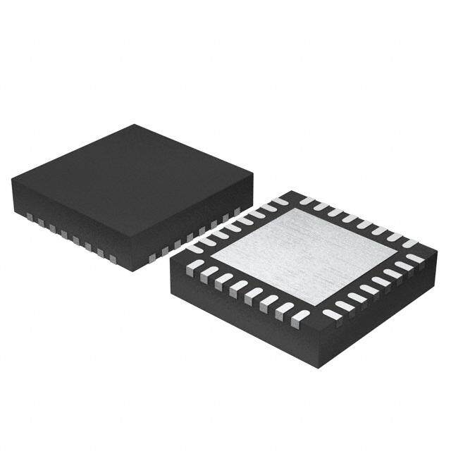
| 描述 | IC SYNTHESIZER VCO 24LFCSP |
| 产品分类 | |
| 品牌 | Analog Devices Inc |
| 数据手册 | |
| 产品图片 |
|
| 产品型号 | ADF4360-2BCPZRL7 |
| PCN组件/产地 | |
| PLL | 是 |
| rohs | 无铅 / 符合限制有害物质指令(RoHS)规范要求 |
| 产品系列 | - |
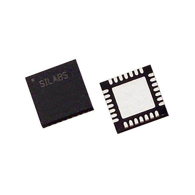
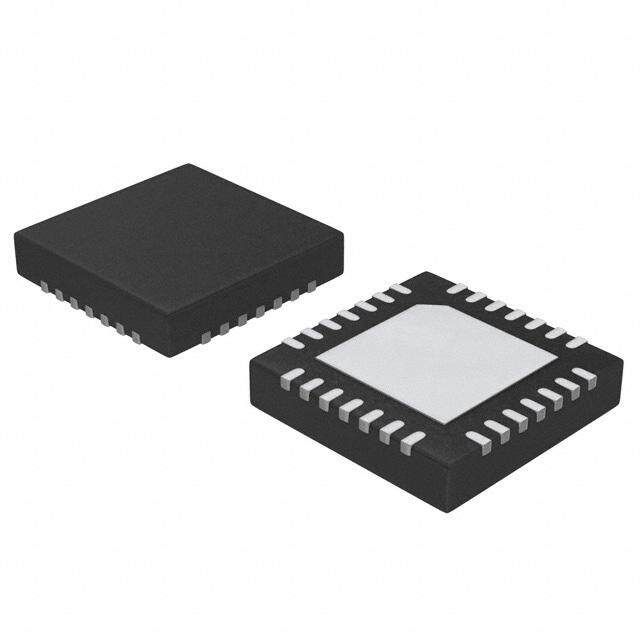
| 供应商器件封装 | 24-LFCSP-VQ(4x4) |
| 其它名称 | ADF4360-2BCPZRL7DKR |
| 分频器/倍频器 | 是/无 |
| 包装 | Digi-Reel® |
| 安装类型 | 表面贴装 |
| 封装/外壳 | 24-VFQFN 裸露焊盘,CSP |
| 工作温度 | -40°C ~ 85°C |
| 差分-输入:输出 | 无/无 |
| 标准包装 | 1 |
| 比率-输入:输出 | 1:2 |
| 电压-电源 | 3 V ~ 3.6 V |
| 电路数 | 1 |
| 类型 | 扇出配送,整数-N,合成器(RF) |
| 输入 | CMOS,TTL |
| 输出 | 时钟 |
| 配用 | /product-detail/zh/EVAL-ADF4360-2EBZ1/EVAL-ADF4360-2EBZ1-ND/1305725 |
| 频率-最大值 | 2.17GHz |


- 商务部:美国ITC正式对集成电路等产品启动337调查
- 曝三星4nm工艺存在良率问题 高通将骁龙8 Gen1或转产台积电
- 太阳诱电将投资9.5亿元在常州建新厂生产MLCC 预计2023年完工
- 英特尔发布欧洲新工厂建设计划 深化IDM 2.0 战略
- 台积电先进制程称霸业界 有大客户加持明年业绩稳了
- 达到5530亿美元!SIA预计今年全球半导体销售额将创下新高
- 英特尔拟将自动驾驶子公司Mobileye上市 估值或超500亿美元
- 三星加码芯片和SET,合并消费电子和移动部门,撤换高东真等 CEO
- 三星电子宣布重大人事变动 还合并消费电子和移动部门
- 海关总署:前11个月进口集成电路产品价值2.52万亿元 增长14.8%


PDF Datasheet 数据手册内容提取
Integrated Synthesizer and VCO Data Sheet ADF4360-2 FEATURES GENERAL DESCRIPTION Output frequency range: 1850 MHz to 2170 MHz The ADF4360-2 is a fully integrated integer-N synthesizer Divide-by-2 output and voltage-controlled oscillator (VCO). The ADF4360-2 is 3.0 V to 3.6 V power supply designed for a center frequency of 2000 MHz. In addition, a 1.8 V logic compatibility divide-by-2 option is available, whereby the user gets an RF Integer-N synthesizer output of between 925 MHz and 1085 MHz. Programmable dual-modulus prescaler 8/9, 16/17, 32/33 Programmable output power level Control of all the on-chip registers is through a simple 3-wire 3-wire serial interface interface. The device operates with a power supply ranging Analog and digital lock detect from 3.0 V to 3.6 V and can be powered down when not in use. Hardware and software power-down mode APPLICATIONS Wireless handsets (DECT, GSM, PCS, DCS, WCDMA) Test equipment Wireless LANs CATV equipment FUNCTIONAL BLOCK DIAGRAM AVDD DVDD CE RSET ADF4360-2 MULTIPLEXER MUXOUT 14-BIT R REFIN COUNTER LOCK MUTE DETECT CLK DATLAE DATA2 4R-EBGITISTER FUL2N4A-CTBTCITIHON CHPUAMRGPE CP PHASE COMPARATOR VVCO VTUNE CC CN INTEGER REGISTER RFOUTA VCO OUTPUT CORE STAGE 13-BIT B COUNTER RFOUTB PRESCALER LOAD P/P+1 LOAD 5-BIT A COUNTER N = (BP + A) ER DIVSEL = 1 ÷2 X E PL ULTI M DIVSEL = 2 04436-001 AGND DGND CPGND Figure 1. Rev. D Document Feedback Information furnished by Analog Devices is believed to be accurate and reliable. However, no responsibility is assumed by Analog Devices for its use, nor for any infringements of patents or other One Technology Way, P.O. Box 9106, Norwood, MA 02062-9106, U.S.A. rights of third parties that may result from its use. Specifications subject to change without notice. No license is granted by implication or otherwise under any patent or patent rights of Analog Devices. Tel: 781.329.4700 ©2004–2016 Analog Devices, Inc. All rights reserved. Trademarks and registered trademarks are the property of their respective owners. Technical Support www.analog.com
ADF4360-2 Data Sheet TABLE OF CONTENTS Features .............................................................................................. 1 MUXOUT and Lock Detect ...................................................... 10 Applications ....................................................................................... 1 Input Shift Register .................................................................... 10 General Description ......................................................................... 1 VCO ............................................................................................. 10 Functional Block Diagram .............................................................. 1 Output Stage ................................................................................ 11 Revision History ............................................................................... 2 Latch Structure ........................................................................... 12 Specifications ..................................................................................... 3 Power-Up ..................................................................................... 16 Timing Characteristics ..................................................................... 5 Control Latch .............................................................................. 18 Absolute Maximum Ratings ............................................................ 6 N Counter Latch ......................................................................... 19 Transistor Count ........................................................................... 6 R Counter Latch ......................................................................... 19 ESD Caution .................................................................................. 6 Applications Information .............................................................. 20 Pin Configuration and Function Descriptions ............................. 7 Direct Conversion Modulator .................................................. 20 Typical Performance Characteristics ............................................. 8 Fixed Frequency LO ................................................................... 21 Circuit Description ........................................................................... 9 Interfacing ................................................................................... 21 Reference Input Section ............................................................... 9 PCB Design Guidelines for Chip Scale Package........................... 22 Prescaler (P/P + 1) ........................................................................ 9 Output Matching ........................................................................ 22 A and B Counters ......................................................................... 9 Outline Dimensions ....................................................................... 23 R Counter ...................................................................................... 9 Ordering Guide .......................................................................... 23 PFD and Charge Pump ................................................................ 9 REVISION HISTORY Changes to Table 1 ............................................................................. 3 5/2016—Rev. C to Rev. D Changes to VCO Section ............................................................... 11 Changed ADF4360 Family to ADF4360-2 and ADSP-21xx to Changes to Control Latch Section ............................................... 18 ADSP-2181 ..................................................................... Throughout Changes to Direct Conversion Modulator Section .................... 20 Changes to Figure 3 .......................................................................... 7 Changes to Ordering Guide .......................................................... 23 Updated Outline Dimensions ....................................................... 23 Changes to Ordering Guide .......................................................... 23 12/2004—Rev. 0 to Rev. A Updated Format .................................................................. Universal 11/2012—Rev. B to Rev. C Changes to Specifications ................................................................. 3 Changes to Table 1 ............................................................................ 4 Changes to Timing Characteristics ................................................. 5 Changes to Table 3 ............................................................................ 6 Changes to Power-Up Section ...................................................... 16 Changes to Figure 3 and Table 4 ..................................................... 7 Added Table 10 ............................................................................... 16 Change to Output Matching Section ........................................... 22 Added Figure 16 ............................................................................. 16 Updated Outline Dimensions ....................................................... 23 Changes to Ordering Guide .......................................................... 23 Changes to Ordering Guide .......................................................... 23 Updated Outline Dimensions ....................................................... 23 4/2006—Rev. A to Rev. B 1/2004—Revision 0: Initial Version Updated Format .................................................................. Universal Changes to Features and General Description ............................. 1 Rev. D | Page 2 of 24
Data Sheet ADF4360-2 SPECIFICATIONS1 AV = DV = V = 3.3 V ± 10%; AGND = DGND = 0 V; T = T to T , unless otherwise noted. DD DD VCO A MIN MAX Table 1. Parameter B Version Unit Test Conditions/Comments REF CHARACTERISTICS IN REF Input Frequency 10/250 MHz min/max For f < 10 MHz, use a CMOS-compatible IN square wave, slew rate > 21 V/µs REF Input Sensitivity 0.7/AV V p-p min/max AC-coupled IN DD 0 to AV V max CMOS-compatible DD REF Input Capacitance 5.0 pF max IN REF Input Current ±100 µA max IN PHASE DETECTOR Phase Detector Frequency2 8 MHz max CHARGE PUMP I Sink/Source3 With R = 4.7 kΩ CP SET High Value 2.5 mA typ Low Value 0.312 mA typ R Range 2.7/10 kΩ SET I Three-State Leakage Current 0.2 nA typ CP Sink and Source Current Matching 2 % typ 1.25 V ≤ V ≤ 2.5 V CP I vs. V 1.5 % typ 1.25 V ≤ V ≤ 2.5 V CP CP CP I vs. Temperature 2 % typ V = 2.0 V CP CP LOGIC INPUTS V , Input High Voltage 1.5 V min INH V , Input Low Voltage 0.6 V max INL I /I , Input Current ±1 µA max INH INL C , Input Capacitance 3.0 pF max IN LOGIC OUTPUTS V , Output High Voltage DV − 0.4 V min CMOS output chosen OH DD I , Output High Current 500 µA max OH V , Output Low Voltage 0.4 V max I = 500 µA OL OL POWER SUPPLIES AV 3.0/3.6 V min/V max DD DV AV DD DD V AV VCO DD AI 4 10 mA typ DD DI 4 2.5 mA typ DD I 4, 5 24.0 mA typ I = 15 mA VCO CORE I 4, 5 29.0 mA typ I = 20 mA VCO CORE I 4 3.5 to 11.0 mA typ RF output stage is programmable RFOUT Low Power Sleep Mode4 7 µA typ Rev. D | Page 3 of 24
ADF4360-2 Data Sheet Parameter B Version Unit Test Conditions/Comments RF OUTPUT CHARACTERISTICS5 VCO Output Frequency 1850/2170 MHz min/max I = 20 mA, RF < 2 GHz CORE I = 15 mA, RF > 2 GHz CORE VCO Sensitivity 57 MHz/V typ Lock Time6 400 µs typ To within 10 Hz of final frequency Frequency Pushing (Open Loop) 6 MHz/V typ Frequency Pulling (Open Loop) 15 kHz typ Into 2.00 VSWR load Harmonic Content (Second) −19 dBc typ Harmonic Content (Third) −37 dBc typ Output Power5, 7 −13/−6 dBm typ Programmable in 3 dB steps (see Table 7) Output Power Variation ±3 dB typ For tuned loads, see the Output Matching section VCO Tuning Range 1.25/2.7 V min/max NOISE CHARACTERISTICS5 VCO Phase-Noise Performance8 −110 dBc/Hz typ At 100 kHz offset from carrier −133 dBc/Hz typ At 1 MHz offset from carrier −141 dBc/Hz typ At 3 MHz offset from carrier −147 dBc/Hz typ At 10 MHz offset from carrier Synthesizer Phase-Noise Floor9 −172 dBc/Hz typ At 25 kHz PFD frequency −163 dBc/Hz typ At 200 kHz PFD frequency −147 dBc/Hz typ At 8 MHz PFD frequency In-Band Phase Noise10, 11 −83 dBc/Hz typ At 1 kHz offset from carrier RMS Integrated Phase Error12 0.64 Degrees typ 100 Hz to 100 kHz Spurious Signals due to PFD Frequency11, 13 −70 dBc typ Level of Unlocked Signal with MTLD Enabled −42 dBm typ 1 Operating temperature range is −40°C to +85°C. 2 Guaranteed by design. Sample tested to ensure compliance. 3 ICP is internally modified to maintain constant loop gain over the frequency range. 4 TA = 25°C; AVDD = DVDD = VVCO = 3.3 V; P = 32. 5 For RF > 2 GHz, these characteristics are guaranteed only for VCO core power = 15 mA. For frequencies < 2 GHz, these characteristics are guaranteed only for VCO core power = 20 mA. 6 Jumping from 2.0 GHz to 2.17 GHz. PFD frequency = 200 kHz; loop bandwidth = 10 kHz. 7 Using 50 Ω resistors to VVCO into a 50 Ω load. For tuned loads, see the Output Matching section. 8 The noise of the VCO is measured in open-loop conditions. 9 The synthesizer phase-noise floor is estimated by measuring the in-band phase noise at the output of the VCO and subtracting 20 log N (where N is the N divider value). 10 The phase noise is measured with the EV-ADF4360-2EB1Z evaluation board and the HP8562E spectrum analyzer. The spectrum analyzer provides the REFIN for the synthesizer; offset frequency = 1 kHz. 11 fREFIN = 10 MHz; fPFD = 200 kHz; N = 10,000; loop bandwidth = 10 kHz. 12 fREFIN = 10 MHz; fPFD = 1 MHz; N = 2000; loop bandwidth = 25 kHz. 13 The spurious signals are measured with the EV-ADF4360-2EB1Z evaluation board and the HP8562E spectrum analyzer. The spectrum analyzer provides the REFIN for the synthesizer; fREFOUT = 10 MHz at 0 dBm. Rev. D | Page 4 of 24
Data Sheet ADF4360-2 TIMING CHARACTERISTICS1 AV = DV = V = 3.3 V ± 10%; AGND = DGND = 0 V; 1.8 V and 3 V logic levels used; T = T to T , unless otherwise noted. DD DD VCO A MIN MAX Table 2. Parameter Limit at T to T (B Version) Unit Test Conditions/Comments MIN MAX t 20 ns min LE Setup Time 1 t 10 ns min DATA to CLOCK Setup Time 2 t 10 ns min DATA to CLOCK Hold Time 3 t 25 ns min CLOCK High Duration 4 t 25 ns min CLOCK Low Duration 5 t 10 ns min CLOCK to LE Setup Time 6 t 20 ns min LE Pulse Width 7 1 See the Power-Up section for the recommended power-up procedure for this device. t t 4 5 CLOCK t t 2 3 DB1 DB0 (LSB) DATA DB23 (MSB) DB22 DB2 (CONTROL BIT C2) (CONTROL BIT C1) t 7 LE t1 t6 LE 04436-002 Figure 2. Timing Diagram Rev. D | Page 5 of 24
ADF4360-2 Data Sheet ABSOLUTE MAXIMUM RATINGS T = 25°C, unless otherwise noted. Stresses at or above those listed under Absolute Maximum A Ratings may cause permanent damage to the product. This is a Table 3. stress rating only; functional operation of the product at these Parameter Rating or any other conditions above those indicated in the operational AV to GND1 −0.3 V to +3.9 V section of this specification is not implied. Operation beyond DD AV to DV −0.3 V to +0.3 V the maximum operating conditions for extended periods may DD DD V to GND −0.3 V to +3.9 V affect product reliability. VCO V to AV −0.3 V to +0.3 V VCO DD This device is a high performance RF integrated circuit with an Digital I/O Voltage to GND −0.3 V to V + 0.3 V DD ESD rating of <1 kV; it is ESD sensitive. Proper precautions Analog I/O Voltage to GND −0.3 V to V + 0.3 V DD should be taken for handling and assembly. REF to GND −0.3 V to V + 0.3 V IN DD Operating Temperature TRANSISTOR COUNT Maximum Junction Temperature 150°C 12,543 (CMOS) and 700 (Bipolar). CSP θ Thermal Impedance JA Paddle Soldered 50°C/W ESD CAUTION Paddle Not Soldered 88°C/W Lead Temperature, Soldering Reflow 260°C 1 GND = AGND = DGND = 0 V. Rev. D | Page 6 of 24
Data Sheet ADF4360-2 PIN CONFIGURATION AND FUNCTION DESCRIPTIONS T U PC EC DNGA VDDDOXUM EL 42 32 22 12 02 91 CPGND1 18DATA AVDD2 17CLK AGND3 ADF4360-2 16REFIN RFOUTA4 TOP VIEW 15DGND (Not to Scale) RFOUTB5 14CN VVCO6 13RSET 7VENUTDNGA8 9DNGA 01DNGA 11DNGA 21CC 04436-003 NOTES 1. THE EXPOSED PAD MUST BE CONNECTED TO AGND. Figure 3. Pin Configuration Table 4. Pin Function Descriptions Pin No. Mnemonic Descriptions 1 CPGND Charge Pump Ground. This is the ground return path for the charge pump. 2 AV Analog Power Supply. This ranges from 3.0 V to 3.6 V. Decoupling capacitors to the analog ground plane DD should be placed as close as possible to this pin. AV must have the same value as DV . DD DD 3, 8 to 11, 22 AGND Analog Ground. This is the ground return path of the prescaler and VCO. 4 RF A VCO Output. The output level is programmable from −6 dBm to −13 dBm. See the Output Matching section OUT for a description of the various output stages. 5 RF B VCO Complementary Output. The output level is programmable from −6 dBm to −13 dBm. See the OUT Output Matching section for a description of the various output stages. 6 V Power Supply for the VCO. This ranges from 3.0 V to 3.6 V. Decoupling capacitors to the analog ground plane VCO should be placed as close as possible to this pin. V must have the same value as AV . VCO DD 7 V Control Input to the VCO. This voltage determines the output frequency and is derived from filtering the CP TUNE output voltage. 12 C Internal Compensation Node. This pin must be decoupled to ground with a 10 nF capacitor. C 13 R Connecting a resistor between this pin and CP sets the maximum charge pump output current for the SET GND synthesizer. The nominal voltage potential at the R pin is 0.6 V. The relationship between I and R is SET CP SET 11.75 I = CPmax R SET where R = 4.7 kΩ, I = 2.5 mA. SET CPmax 14 C Internal Compensation Node. This pin must be decoupled to V with a 10 µF capacitor. N VCO 15 DGND Digital Ground. 16 REF Reference Input. This is a CMOS input with a nominal threshold of V /2 and a dc equivalent input resistance of IN DD 100 kΩ. See Figure 10. This input can be driven from a TTL or CMOS crystal oscillator, or it can be ac-coupled. 17 CLK Serial Clock Input. This serial clock is used to clock in the serial data to the registers. The data is latched into the 24-bit shift register on the CLK rising edge. This input is a high impedance CMOS input. 18 DATA Serial Data Input. The serial data is loaded MSB first with the two LSBs being the control bits. This input is a high impedance CMOS input. 19 LE Load Enable, CMOS Input. When LE goes high, the data stored in the shift registers is loaded into one of the four latches, and the relevant latch is selected using the control bits. 20 MUXOUT This multiplexer output allows either the lock detect, the scaled RF, or the scaled reference frequency to be accessed externally. 21 DV Digital Power Supply. This ranges from 3.0 V to 3.6 V. Decoupling capacitors to the digital ground plane DD should be placed as close as possible to this pin. DV must have the same value as AV . DD DD 23 CE Chip Enable. A logic low on this pin powers down the device and puts the charge pump into three-state mode. Taking the pin high powers up the device depending on the status of the power-down bits. 24 CP Charge Pump Output. When enabled, this provides ± I to the external loop filter, which in turn drives the CP internal VCO. EP Exposed Pad. The exposed pad must be connected to AGND. Rev. D | Page 7 of 24
ADF4360-2 Data Sheet TYPICAL PERFORMANCE CHARACTERISTICS 0 0 –10 VDD = 3V, VVCO = 3V –20 –10 ICP = 2.5mA –30 PFD FREQUENCY = 200kHz –20 LOOP BANDWIDTH = 10kHz –40 RES. BANDWIDTH = 30Hz dB) ––5600 dB) –30 VSIWDEEEOP B =A 1N.D9SWEICDOTHN D= S30Hz R ( –70 1 R ( –40 AVERAGES = 10 E E W –80 W PO –90 PO –50 UT –100 2 UT –60 –84.0dBc/Hz TP–110 TP OU–120 3 OU –70 –130 4 –140 –80 –––111567000 04436-004 –90 04436-007 1k 10k 100k 1M 10M –2kHz –1kHz 2000MHz 1kHz 2kHz FREQUENCY OFFSET (Hz) Figure 4. Open-Loop VCO Phase Noise Figure 7. Close-In Phase Noise at 2000 MHz (200 kHz Channel Spacing) –70 0 –75 VDD = 3V, VVCO = 3V –80 –10 ICP = 2.5mA PFD FREQUENCY = 200kHz –85 –20 LOOP BANDWIDTH = 10kHz –90 RES. BANDWIDTH = 3kHz R (dB)––10905 R (dB) ––4300 VSAIWVDEEEREOAP BG =AE 1NS4D 0=Wm 1I0sD0TH = 3kHz E–105 E W W O–110 O –50 P P T –115 T TPU–120 TPU –60 –79.5dBc OU–125 OU –70 –130 –135 –80 –––111454500 04436-005 –90 04436-008 100 1k 10k 100k 1M 10M –200kHz –100kHz 2000MHz 100kHz 200kHz FREQUENCY OFFSET (Hz) Figure 5. VCO Phase Noise, 2000 MHz, 200 kHz PFD, 10 kHz Loop Bandwidth Figure 8. Reference Spurs at 2000 MHz (200 kHz Channel Spacing, 10 kHz Loop Bandwidth) –70 0 –75 VDD = 3V, VVCO = 3V –80 –10 ICP = 2.5mA PFD FREQUENCY = 1MHz –85 –20 LOOP BANDWIDTH = 25kHz –90 RES. BANDWIDTH = 30kHz R (dB)––19050 R (dB) ––4300 VSAIWVDEEEREOAP BG =AE 5NS0D m=W 1sI0D0TH = 30kHz E–105 E W W O–110 O –50 P P T –115 T PU–120 PU –60 OUT–125 OUT –70 –83.8dBc/Hz –130 –135 –80 –––111454500 04436-006 –90 04436-009 100 1k 10k 100k 1M 10M –1MHz –0.5MHz 2000MHz 0.5MHz 1MHz FREQUENCY OFFSET (Hz) Figure 6. VCO Phase Noise, 1000 MHz, Figure 9. Reference Spurs at 2000 MHz Divide-by-2 Enabled 200 kHz PFD, 10 kHz Loop Bandwidth (1 MHz Channel Spacing, 25 kHz Loop Bandwidth) Rev. D | Page 8 of 24
Data Sheet ADF4360-2 CIRCUIT DESCRIPTION REFERENCE INPUT SECTION N = BP + A The reference input stage is shown in Figure 10. SW1 and SW2 13-BIT B TO PFD COUNTER are normally closed switches. SW3 is normally open. When LOAD power-down is initiated, SW3 is closed, and SW1 and SW2 are PRESCALER FROM VCO P/P+1 opened. This ensures that there is no loading of the REF pin LOAD IN on power-down. MODULUS 5-BIT A CONTROL COUNTER POCWOENRT-RDOOLWN N DIVIDER 04436-011 NC 100kΩ Figure 11. A and B Counters SW2 REFIN NC TO R COUNTER R COUNTER BUFFER SW1 NO SW3 04436-010 Tbeh ed i1v4id-beidt Rdo cwonu ntote pr raolldouwcse tthhee irnepfeurte rnecfee rcelnoccek ftroe qthuee npchya steo Figure 10. Reference Input Stage frequency detector (PFD). Division ratios from 1 to 16,383 are allowed. PRESCALER (P/P + 1) PFD AND CHARGE PUMP The dual-modulus prescaler (P/P + 1), along with the A and B counters, enables the large division ratio, N, to be realized The PFD takes inputs from the R counter and N counter (N = BP + A). The dual-modulus prescaler, operating at CML (N = BP + A) and produces an output proportional to the phase levels, takes the clock from the VCO and divides it down to a and frequency difference between them. Figure 12 is a simplified manageable frequency for the CMOS A and B counters. The schematic. The PFD includes a programmable delay element prescaler is programmable. It can be set in software to 8/9, that controls the width of the antibacklash pulse. This pulse 16/17, or 32/33 and is based on a synchronous 4/5 core. There is ensures that there is no dead zone in the PFD transfer function a minimum divide ratio possible for fully contiguous output and minimizes phase noise and reference spurs. Two bits in the frequencies; this minimum is determined by P, the prescaler R counter latch, ABP2 and ABP1, control the width of the pulse value, and is given by (P2 − P). (see Table 9). A AND B COUNTERS VP CHARGE PUMP The A and B CMOS counters combine with the dual-modulus UP HI D1 Q1 prescaler to allow a wide range division ratio in the PLL feedback U1 counter. The counters are specified to work when the prescaler output is 300 MHz or less. Thus, with a VCO frequency of R DIVIDER CLR1 2.5 GHz, a prescaler value of 16/17 is valid, but a value of 8/9 is not valid. PROGRAMMABLE U3 CP DELAY Pulse Swallow Function The A and B counters, in conjunction with the dual-modulus ABP1 ABP2 prescaler, make it possible to generate output frequencies that CLR2 are spaced only by the reference frequency divided by R. The DOWN HI D2 Q2 VCO frequency equation is U2 f = ((P × B) + A) × f /R VCO REFIN N DIVIDER CPGND where: f is the output frequency of the VCO. VCO P is the preset modulus of the dual-modulus prescaler (8/9, R DIVIDER 16/17, and so on). N DIVIDER B is the preset divide ratio of the binary 13-bit counter (3 to 8,191). A is the preset divide ratio of the binary 5-bit swallow counter (0 to 31). CP OUTPUT 04436-012 fREFIN is the external reference frequency oscillator. Figure 12. PFD Simplified Schematic and Timing (In Lock) Rev. D | Page 9 of 24
ADF4360-2 Data Sheet MUXOUT AND LOCK DETECT Table 5. C2 and C1 Truth Table Control Bits The output multiplexer on the ADF4360-2 allows the user to C2 C1 Data Latch access various internal points on the chip. The state of 0 0 Control Latch MUXOUT is controlled by M3, M2, and M1 in the function 0 1 R Counter latch. The full truth table is shown in Table 7. Figure 13 shows 1 0 N Counter (A and B) the MUXOUT section in block diagram form. 1 1 Test Mode Latch Lock Detect MUXOUT can be programmed for two types of lock detect: VCO digital and analog. Digital lock detect is active high. When LDP The VCO core in the ADF4360-2 uses eight overlapping bands, in the R counter latch is set to 0, digital lock detect is set high as shown in Figure 14, to allow a wide frequency range to be when the phase error on three consecutive phase detector cycles covered without a large VCO sensitivity (K ) and resultant poor V is less than 15 ns. phase noise and spurious performance. With LDP set to 1, five consecutive cycles of less than 15 ns The correct band is chosen automatically by the band select phase error are required to set the lock detect. It stays set high logic at power-up or whenever the N counter latch is updated. It until a phase error of greater than 25 ns is detected on any is important that the correct write sequence be followed at subsequent PD cycle. power-up. This sequence is The N-channel, open-drain, analog lock detect should be 1. R counter latch operated with an external pull-up resistor of 10 kΩ nominal. 2. Control latch When a lock is detected, the output is high with narrow low- 3. N counter latch going pulses. During band select, which takes five PFD cycles, the VCO V DVDD TUNE is disconnected from the output of the loop filter and is connected to an internal reference voltage. ANALOG LOCK DETECT DIGITAL LOCK DETECT 3.5 R COUNTER OUTPUT MUX CONTROL MUXOUT 3.0 N COUNTER OUTPUT SDOUT 2.5 DGND 04436-013 LTAGE (V) 12..50 Figure 13. MUXOUT Circuit O V 1.0 INPUT SHIFT REGISTER Tshhieft drieggiitsatle sr,e cat 1io4n-b oitf Rth ceo AuDntFe4r,3 a6n0d-2 a inn 1cl8u-dbeits Na 2c4o-ubnitt eirn p ut 0.05 04436-014 comprised of a 5-bit A counter and a 13-bit B counter. Data is 1600 1700 1800 1900 2000 2100 2200 2300 clocked into the 24-bit shift register on each rising edge of CLK. FREQUENCY (MHz) The data is clocked in MSB first. Data is transferred from the Figure 14. Frequency vs. VTUNE, ADF4360-2 shift register to one of four latches on the rising edge of LE. The The R counter output is used as the clock for the band select destination latch is determined by the state of the two control logic and should not exceed 1 MHz. A programmable divider is bits (C2, C1) in the shift register. The two LSBs are DB1 and provided at the R counter input to allow division by 1, 2, 4, or 8 DB0, as shown in Figure 2. and is controlled by Bit BSC1 and Bit BSC2 in the R counter latch. The truth table for these bits is shown in Table 5. Table 6 shows Where the required PFD frequency exceeds 1 MHz, the divide ratio a summary of how the latches are programmed. Note that the should be set to allow enough time for correct band selection. test mode latch is used for factory testing and should not be After band selection, normal PLL action resumes. The nominal programmed by the user. value of K is 57 MHz/V, or 28 MHz/V if divide-by-2 operation V is selected (by programming DIV2 [DB22] high in the N counter latch). The ADF4360-2 contains linearization circuitry to minimize any variation of the product of I and K . CP V Rev. D | Page 10 of 24
Data Sheet ADF4360-2 The operating current in the VCO core is programmable in four If the outputs are used individually, the optimum output stage steps: 5 mA, 10 mA, 15 mA, and 20 mA. This is controlled by consists of a shunt inductor to V . DD Bit PC1 and Bit PC2 in the control latch. For VCO frequencies above 2 GHz, only the 15 mA core current should be used, and Another feature of the ADF4360-2 is that the supply current to for frequencies below 2 GHz, only 20 mA core current should the RF output stage is shut down until the device achieves lock be used. as measured by the digital lock detect circuitry. This is enabled by the mute-till-lock detect (MTLD) bit in the control latch. OUTPUT STAGE RFOUTA RFOUTB The RF A and RF B pins of the ADF4360-2 are connected OUT OUT to the collectors of an NPN differential pair driven by buffered outputs of the VCO, as shown in Figure 15. To allow the user to optimize the power dissipation vs. the output power requirements, VCO BUFFER/ the tail current of the differential pair is programmable via Bit PL1 DIVIDE-BY-2 and Bit PL2 in the control latch. Four current levels can be set: 3p.o5w merA l,e 5v emlsA o,f 7−.153 m dAB,m a,n −d1 111 d mBAm., T−h8e dseB mlev, ealnsd g i−v6e doButmpu, t 04436-015 respectively, using a 50 Ω resistor to V and ac coupling into a Figure 15. Output Stage ADF4360-2 DD 50 Ω load. Alternatively, both outputs can be combined in a 1 + 1:1 transformer or a 180° microstrip coupler (see the Output Matching section). Rev. D | Page 11 of 24
ADF4360-2 Data Sheet LATCH STRUCTURE Table 6 shows the three on-chip latches for the ADF4360-2. The two LSBs determines which latch is programmed. Table 6. Latch Structure CONTROL LATCH PRVEASCLUAELER POWER-DOWN 2 POWER-DOWN 1 SCEUTRTRINEGNT2 SCEUTRTRINEGNT1 OPLUOETWVPEEULRT MUTE-TILL-LD CP GAIN CPTHREE-STATEPHASEDETECTORPOLARITY CMOUNXTORUOTL COUNTERRESET PLCOEOWVREEELR COBNITTRSOL DB23 DB22 DB21 DB20 DB19 DB18 DB17 DB16 DB15 DB14 DB13 DB12 DB11 DB10 DB9 DB8 DB7 DB6 DB5 DB4 DB3 DB2 DB1 DB0 P2 P1 PD2 PD1 CPI6 CPI5 CPI4 CPI3 CPI2 CPI1 PL2 PL1 MTLD CPG CP PDP M3 M2 M1 CR PC2 PC1 C2 (0)C1 (0) N COUNTER LATCH DIVIDE-BY-2 SELECT DIVIDE-BY-2 CP GAIN 13-BIT B COUNTER RESERVED 5-BIT A COUNTER COBNITTRSOL DB23 DB22 DB21 DB20 DB19 DB18 DB17 DB16 DB15 DB14 DB13 DB12 DB11 DB10 DB9 DB8 DB7 DB6 DB5 DB4 DB3 DB2 DB1 DB0 DIVSEL DIV2 CPG B13 B12 B11 B10 B9 B8 B7 B6 B5 B4 B3 B2 B1 RSV A5 A4 A3 A2 A1 C2 (1)C1 (0) R COUNTER LATCH D D RESERVE RESERVE SCBELALONECCDKT TESTMODEBITLOCKDETECTPRECISION BAPWCAUIKNDLLTTSAIH-ESH 14-BIT REFERENCE COUNTER COBNITTRSOL DB23 DB22 DB21 DB20 DB19 DB18 DB17 DB16 DB15 DB14 DB13 DB12 DB11 DB10 DB9 DB8 DB7 DB6 DB5 DB4 DB3 DB2 DB1 DB0 RSV RSV BSC2 BSC1 TMB LDP ABP2 ABP1 R14 R13 R12 R11 R10 R9 R8 R7 R6 R5 R4 R3 R2 R1 C2 (0)C1 (1) 04436-016 Rev. D | Page 12 of 24
Data Sheet ADF4360-2 Table 7. Control Latch PREVASLCUAELER POWER-DOWN 2 POWER-DOWN 1 SCEUTRTRINEGNT2 SCEUTRTRINEGNT1 OPLUOETWVPEEULRT MUTE-TILL-LD CP GAIN CPTHREE-STATEPHASEDETECTORPOLARITY CMOUNXTORUOTL COUNTERRESET PLCOEOWVREEELR COBNITTRSOL DB23 DB22 DB21 DB20 DB19 DB18 DB17 DB16 DB15 DB14 DB13 DB12 DB11 DB10 DB9 DB8 DB7 DB6 DB5 DB4 DB3 DB2 DB1 DB0 P2 P1 PD2 PD1 CPI6 CPI5 CPI4 CPI3 CPI2 CPI1 PL2 PL1 MTLD CPG CP PDP M3 M2 M1 CR PC2 PC1 C2(0)C1(0) PC2 PC1 COREPOWER LEVEL 0 0 5mA 0 1 10mA 1 0 15mA 1 1 20mA CPI6 CPI5 CPI4 ICP(mA) PHASEDETECTOR C00PI3 C00PI2 01CPI1 004...36712kΩ P01DP PNPOOEGSLIAATTRIVIIVETEY C0R CONOOPEURRNMATATELIRON 0 1 0 0.93 1 R,A,BCOUNTERS 0 1 1 1.25 CHARGEPUMP HELD INRESET 1 0 0 1.56 CP OUTPUT 1 0 1 1.87 0 NORMAL 1 1 0 2.18 1 THREE-STATE 1 1 1 2.50 CPG CP GAIN 0 CURRENTSETTING1 1 CURRENTSETTING2 MTLD MUTE-TILL-LOCKDETECT 0 DISABLED 1 ENABLED PL2 PL1 OUTPUTPOWERLEVEL M3 M2 M1 OUTPUT CURRENT POWER INTO50Ω(USING50ΩTOVVCC) 0 0 0 THREE-STATE OUTPUT 0 0 3.5mA –13dBm 0 0 1 DIGITALLOCKDETECT (ACTIVEHIGH) 0 1 5.0mA –11dBm 1 0 7.5mA –8dBm 0 1 0 NDIVIDER OUTPUT 1 1 11.0mA –6dBm 0 1 1 DVDD 1 0 0 RDIVIDER OUTPUT 1 0 1 N-CHANNEL OPEN-DRAIN LOCKDETECT 1 1 0 SERIALDATA OUTPUT 1 1 1 DGND CEPIN PD2 PD1 MODE 0 X X ASYNCHRONOUSPOWER-DOWN 1 X 0 NORMAL OPERATION 1 0 1 ASYNCHRONOUSPOWER-DOWN 1 1 1 SYNCHRONOUSPOWER-DOWN P2 P1 PRESCALERVALUE 0 0 8/9 101 110 331226///331337 04436-017 Rev. D | Page 13 of 24
ADF4360-2 Data Sheet Table 8. N Counter Latch DIVIDE-BY-2 SELECT DIVIDE-BY-2 CP GAIN 13-BIT B COUNTER RESERVED 5-BIT A COUNTER COBNITTRSOL DB23 DB22 DB21 DB20 DB19 DB18 DB17 DB16 DB15 DB14 DB13 DB12 DB11 DB10 DB9 DB8 DB7 DB6 DB5 DB4 DB3 DB2 DB1 DB0 DIVSEL DIV2 CPG B13 B12 B11 B10 B9 B8 B7 B6 B5 B4 B3 B2 B1 RSV A5 A4 A3 A2 A1 C2 (1)C1 (0) THIS BIT IS NOT USED BY THE DEVICEAND IS A DON'T CARE BIT. A COUNTER A5 A4 .......... A2 A1 DIVIDE RATIO 0 0 .......... 0 0 0 0 0 .......... 0 1 1 0 0 .......... 1 0 2 0 0 .......... 1 1 3 . . .......... . . . . . .......... . . . . . .......... . . . 1 1 .......... 0 0 28 1 1 .......... 0 1 29 1 1 .......... 1 0 30 1 1 .......... 1 1 31 B13 B12 B11 B3 B2 B1 B COUNTER DIVIDE RATIO 0 0 0 .......... 0 0 0 NOTALLOWED 0 0 0 .......... 0 0 1 NOTALLOWED 0 0 0 .......... 0 1 0 NOTALLOWED 0 0 0 .......... 1 1 1 3 . . . .......... . . . . . . . .......... . . . . . . . .......... . . . . 1 1 1 .......... 1 0 0 8188 1 1 1 .......... 1 0 1 8189 1 1 1 .......... 1 1 0 8190 1 1 1 .......... 1 1 1 8191 F4 (FUNCTION LATCH) FASTLOCK ENABLE CP GAIN OPERATION 0 0 CHARGE PUMP CURRENT SETTING 1 IS PERMANENTLY USED 0 1 CHARGE PUMP CURRENT SETTING 2 IS PERMANENTLY USED N = BP +A;P IS PRESCALERVALUE SET IN THE CONTROL LATCH. BA DMJUASCTE NBTE VGARLEUAETSE RO FT H(NA N× FORRE FE)Q,AUTA TLHTEO OAU. TFPOURT C, NOMNITN IINSU (OP2U–SPL)Y. 04436-018 DIV2 DIVIDE-BY-2 0 FUNDAMENTAL OUTPUT 1 DIVIDE-BY-2 DIVSEL DIVIDE-BY-2 SELECT (PRESCALER INPUT) 0 FUNDAMENTAL OUTPUT SELECTED 1 DIVIDE-BY-2 SELECTED Rev. D | Page 14 of 24
Data Sheet ADF4360-2 Table 9. R Counter Latch D D RESERVE RESERVE SCBELALONECCDKT TESTMODEBITLOCKDETECTPRECISION BAPWCAUIKNDLLTTSAIH-ESH 14-BIT REFERENCE COUNTER COBNITTRSOL DB23 DB22 DB21 DB20 DB19 DB18 DB17 DB16 DB15 DB14 DB13 DB12 DB11 DB10 DB9 DB8 DB7 DB6 DB5 DB4 DB3 DB2 DB1 DB0 RSV RSV BSC2 BSC1 TMB LDP ABP2 ABP1 R14 R13 R12 R11 R10 R9 R8 R7 R6 R5 R4 R3 R2 R1 C2 (0)C1 (1) R14 R13 R12 R3 R2 R1 DIVIDE RATIO 0 0 0 .......... 0 0 0 1 0 0 0 .......... 0 1 1 2 0 0 0 .......... 0 1 0 3 TEST MODE 0 0 0 .......... 1 0 1 4 BIT SHOULD . . . .......... . . . . BE SET TO 0 . . . .......... . . . . THESE BITS ARE NOT FOR NORMAL . . . .......... . . . . USED BY THE DEVICE OPERATION. 1 1 1 .......... 1 0 0 16380 AND ARE DON'T CARE 1 1 1 .......... 1 0 1 16381 BITS. 1 1 1 .......... 1 1 0 16382 1 1 1 .......... 1 1 1 16383 ABP2 ABP1 ANTIBACKLASH PULSE WIDTH 0 0 3.0ns 0 1 1.3ns 1 0 6.0ns 1 1 3.0ns LDP LOCK DETECT PRECISION 0 THREE CONSECUTIVE CYCLES OF PHASE DELAY LESS THAN 15ns MUST OCCUR BEFORE LOCK DETECT IS SET. 1 FIVE CONSECUTIVE CYCLES OF PHASE DELAY LESS THAN 15ns MUST OCCUR BEFORE LOCK DETECT IS SET. BSC2 BSC1 BAND SELECT CLOCK DIVIDER 0 0 1 011 101 482 04436-019 Rev. D | Page 15 of 24
ADF4360-2 Data Sheet POWER-UP This interval is necessary to allow the transient behavior of the Power-Up Sequence ADF4360-2 during initial power-up to have settled. During initial power-up, a write to the control latch powers up the The correct programming sequence for the ADF4360-2 after device and the bias currents of the VCO begin to settle. If these power-up is as: currents have not settled to within 10% of their steady-state 1. R counter latch value, and if the N counter latch is then programmed, the VCO 2. Control latch may not be able to oscillate at the desired frequency, which does 3. N counter latch not allow the band select logic to choose the correct frequency band and the ADF4360-2 may not achieve lock. If the Initial Power-Up recommended interval is inserted and the N counter latch is Initial power-up refers to programming the device after the programmed, the band select logic can choose the correct application of voltage to the AV , DV , V , and CE pins. On frequency band, and the device locks to the correct frequency. DD DD VCO initial power-up, an interval is required between programming The duration of this interval is affected by the value of the the control latch and programming the N counter latch. capacitor on the C pin (Pin 14). This capacitor is used to N reduce the close-in noise of the ADF4360-2 VCO. The recommended value of this capacitor is 10 µF. Using this value requires an interval of ≥ 5 ms between the latching in of the control latch bits and the latching in of the N counter latch bits. If a shorter delay is required, this capacitor can be reduced. A slight phase noise penalty is incurred by this change, which is explained further in Table 10. Table 10. C Capacitance vs. Interval and Phase Noise N C Value Recommended Interval Between Control Latch and N Counter Latch Open-Loop Phase Noise at 10 kHz Offset N 10 µF ≥ 5 ms −86 dBc 440 nF ≥ 600 µs −85 dBc POWER-UP CLOCK R COUNTER CONTROL N COUNTER DATA LATCH DATA LATCH DATA LATCH DATA LE CNO CNROTERUQONULTIR ELERAD TL CIANHTT CWEHRR VWITARELI TTEO 04436-020 Figure 16. ADF4360-2 Power-Up Timing Rev. D | Page 16 of 24
Data Sheet ADF4360-2 Hardware Power-Up/Power-Down Software Power-Up/Power-Down If the ADF4360-2 is powered down via the hardware (using the If the ADF4360-2 is powered down via the software (using the CE pin) and powered up again without any change to the N control latch) and powered up again without any change to the counter register during power-down, the device locks at the N counter latch during power-down, the device locks at the correct frequency because it is already in the correct frequency correct frequency because it is already in the correct frequency band. The lock time depends on the value of capacitance on the band. The lock time depends on the value of capacitance on the C pin, which is <5 ms for 10 µF capacitance. The smaller C pin, which is <5 ms for 10 µF capacitance. The smaller N N capacitance of 440 nF on this pin enables lock times of <600 µs. capacitance of 440 nF on this pin enables lock times of <600 µs. The N counter value cannot be changed while it is in power- The N counter value cannot be changed while the device is in down because it may not lock to the correct frequency on power-down because it may not lock to the correct frequency power-up. If it is updated, the correct programming sequence on power-up. If it is updated, the correct programming sequence for the device after power-up is to the R counter latch, followed for the devices after power-up is to the R counter latch, followed by the control latch, and finally the N counter latch, with the by the control latch, and finally the N counter latch, with the required interval between the control latch and N counter latch, required interval between the control latch and N counter latch, as described in the Initial Power-Up section. as described in the Initial Power-Up section. Rev. D | Page 17 of 24
ADF4360-2 Data Sheet CONTROL LATCH Charge Pump Currents With (C2, C1) = (0, 0), the control latch is programmed. Table 7 CPI3, CPI2, and CPI1 in the ADF4360-2 determine shows the input data format for programming the control latch. Current Setting 1. Prescaler Value CPI6, CPI5, and CPI4 determine Current Setting 2. See the truth table in Table 7. In the ADF4360-2, P2 and P1 in the control latch set the prescaler values. Output Power Level Power-Down Bit PL1 and Bit PL2 set the output power level of the VCO. See the truth table in Table 7. DB21 (PD2) and DB20 (PD1) provide programmable power- down modes. Mute-Till-Lock Detect (LD) In the programmed asynchronous power-down, the device DB11 of the control latch in the ADF4360-2 is the mute-till- powers down immediately after latching a 1 into Bit PD1, with lock detect bit. This function, when enabled, ensures that the the condition that PD2 is loaded with a 0. In the programmed RF outputs are not switched on until the PLL is locked. synchronous power-down, the device power-down is gated by CP Gain the charge pump to prevent unwanted frequency jumps. Once DB10 of the control latch in the ADF4360-2 is the charge pump the power-down is enabled by writing a 1 into Bit PD1 (on the gain bit. When it is programmed to 1, Current Setting 2 is used. condition that a 1 is also loaded to PD2), the device goes into When it is programmed to 0, Current Setting 1 is used. power-down on the second rising edge of the R counter output, after LE goes high. When the CE pin is low, the device is Charge Pump (CP) Three-State immediately disabled regardless of the state of PD1 or PD2. This bit puts the charge pump into three-state mode when When a power-down is activated (either synchronous or programmed to a 1. It should be set to 0 for normal operation. asynchronous mode), the following events occur: Phase Detector Polarity • All active dc current paths are removed. The PDP bit in the ADF4360-2 sets the phase detector polarity. • The R, N, and timeout counters are forced to their load The positive setting enabled by programming a 1 is used when state conditions. using the on-chip VCO with a passive loop filter or with an • The charge pump is forced into three-state mode. active noninverting filter. It can also be set to 0, which is • The digital lock detect circuitry is reset. required if an active inverting loop filter is used. • The RF outputs are debiased to a high impedance state. MUXOUT Control • The reference input buffer circuitry is disabled. The on-chip multiplexer is controlled by M3, M2, and M1. • The input register remains active and capable of loading See the truth table in Table 7. and latching data. Counter Reset DB4 is the counter reset bit for the ADF4360-2. When this is 1, the R counter and the A, B counters are reset. For normal operation, this bit should be 0. Core Power Level PC1 and PC2 set the power level in the VCO core. The recommended setting is 15 mA for frequencies above 2 GHz and 20 mA for frequencies below 2 GHz. No other settings are valid. See the truth table in Table 7. Rev. D | Page 18 of 24
Data Sheet ADF4360-2 N COUNTER LATCH R COUNTER LATCH With (C2, C1) = (1, 0), the N counter latch is programmed. With (C2, C1) = (0, 1), the R counter latch is programmed. Table 8 shows the input data format for programming the Table 9 shows the input data format for programming the N counter latch. R counter latch. A Counter Latch R Counter A5 to A1 program the 5-bit A counter. The divide range is R1 to R14 set the counter divide ratio. The divide range is 0 (00000) to 31 (11111). 1 (00......001) to 16383 (111......111). Reserved Bits Antibacklash Pulse Width DB7 is a spare bit that is reserved. It should be programmed to 0. DB16 and DB17 set the antibacklash pulse width. B Counter Latch Lock Detect Precision B13 to B1 program the B counter. The divide range is 3 DB18 is the lock detect precision bit. This bit sets the number of (00.....0011) to 8191 (11....111). reference cycles with less than 15 ns phase error for entering the locked state. With LDP at 1, five cycles are taken; with LDP at 0, Overall Divide Range three cycles are taken. The overall divide range is defined by ((P × B) + A), where P is Test Mode Bit (TMB) the prescaler value. DB19 is the test mode bit and should be set to 0. With TMB = 0, CP Gain the contents of the test mode latch are ignored and normal DB21 of the N counter latch in the ADF4360-2 is the charge operation occurs as determined by the contents of the control pump gain bit. When this bit is programmed to 1, Current latch, R counter latch, and N counter latch. Note that test modes Setting 2 is used. When programmed to 0, Current Setting 1 is are for factory testing only and should not be programmed by used. This bit can also be programmed through DB10 of the the user. control latch. The bit always reflects the latest value written to it, Band Select Clock whether through the control latch or the N counter latch. These bits set a divider for the band select logic clock input. The Divide-by-2 output of the R counter is by default the value used to clock the DB22 is the divide-by-2 bit. When set to 1, the output divide-by-2 band select logic. If this value is too high (>1 MHz), a divider function is chosen. When set to 0, normal operation occurs. can be switched on to divide the R counter output to a smaller value (see Table 9). Divide-by-2 Select DB23 is the divide-by-2 select bit. When programmed to 1, the Reserved Bits divide-by-2 output is selected as the prescaler input. When set DB23 to DB22 are spare bits that are reserved. They should be to 0, the fundamental is used as the prescaler input. For programmed to 0. example, using the output divide-by-2 feature and a PFD frequency of 200 kHz, the user needs a value of N = 10,000 to generate 1000 MHz. With the divide-by-2 select bit high, the user can keep N = 5000. Rev. D | Page 19 of 24
ADF4360-2 Data Sheet APPLICATIONS INFORMATION DIRECT CONVERSION MODULATOR The LO ports of the AD8349 can be driven differentially from the complementary RF A and RF B outputs of the Direct conversion architectures are increasingly being used to OUT OUT ADF4360-2. This gives better performance than a single-ended implement base station transmitters. Figure 17 shows how LO driver and eliminates the often necessary use of a balun to Analog Devices, Inc., devices can be used to implement such a convert from a single-ended LO input to the more desirable system. differential LO inputs for the AD8349. The typical rms phase The circuit block diagram shows the AD9761 TxDAC® being noise (100 Hz to 100 kHz) of the LO in this configuration is 2.1°. used with the AD8349. The use of dual integrated DACs, such The AD8349 accepts LO drive levels from −10 dBm to 0 dBm. as the AD9761 with its specified ±0.02 dB and ±0.004 dB gain The optimum LO power can be software programmed on the and offset matching characteristics, ensures minimum error ADF4360-2, which allows levels from −13 dBm to −6 dBm from contribution (over temperature) from this portion of the signal each output. chain. The RF output is designed to drive a 50 Ω load but must be ac- The local oscillator is implemented using the ADF4360-2. The coupled, as shown in Figure 17. If the I and Q inputs are driven low-pass filter was designed using ADIsimPLL™ for a channel in quadrature by 2 V p-p signals, the resulting output power spacing of 100 kHz and an open-loop bandwidth of 10 kHz. from the modulator is approximately 2 dBm. The frequency range of the ADF4360-2 (1.85 GHz to 2.17 GHz) makes it ideally suited for the implementation of a W-CDMA transceiver. REFIO IOUTA LOW-PASS MODULATED AD9761 IOUTB FILTER DIGITAL TxDAC DATA QOUTA LOW-PASS QOUTB FILTER FSADJ 2kΩ LOCK VVCO VDD DETECT VPS1 VPS2 IBBP 10µF 6 21 2 23 20 1nF1nF 14 CVNVCO DVDD AVDD CE MUXOUT VTUCNPE 274 13kΩ IBBN 100pF FREFIN 16 REFIN 6.8nF 51Ω 470pF 220pF TO 6.8kΩ AD8349 RFPA 17 CLK ADF4360-2 QBBP 18 DATA VVCO 19 LE BUS 12 CC 47nH 47nH QBBN AL 1nF 13 RSET 1.8pF 3.6nH LOIP ERI 4.7kΩ RFOUTA 4 PHASE PATIBLE S CP1GND3 8 A9GN1D0 11 22DG15ND RFOUTB 5 1.8pF 3.6nH LOIN SPLITTER 04436-021 M O C PI- S Figure 17. Direct Conversion Modulator Rev. D | Page 20 of 24
Data Sheet ADF4360-2 FIXED FREQUENCY LO ADuC812 Interface Figure 18 shows the ADF4360-2 used as a fixed frequency LO at Figure 19 shows the interface between the ADF4360-2 and the 2.0 GHz. The low-pass filter was designed using ADIsimPLL ADuC812 MicroConverter®. Because the ADuC812 is based on for a channel spacing of 8 MHz and an open-loop bandwidth of an 8051 core, this interface can be used with any 8051-based 40 kHz. The maximum PFD frequency of the ADF4360-2 is microcontroller. The MicroConverter is set up for SPI master 8 MHz. Because using a larger PFD frequency allows the use of a mode with CPHA = 0. To initiate the operation, the I/O port smaller N, the in-band phase noise is reduced to as low as driving LE is brought low. Each latch of the ADF4360-2 needs a possible, –99 dBc/Hz. The 40 kHz bandwidth is chosen to be just 24-bit word, which is accomplished by writing three 8-bit bytes greater than the point at which the open-loop phase noise of the from the MicroConverter to the device. When the third byte is VCO is –99 dBc/Hz, thus giving the best possible integrated written, the LE input should be brought high to complete the noise. The typical rms phase noise (100 Hz to 100 kHz) of the LO transfer. in this configuration is 0.3°. The reference frequency is from a 16 MHz TCXO from Fox; thus, an R value of 2 is programmed. Taking into account the high PFD frequency and its effect on the SCLOCK SCLK band select logic, the band select clock divider is enabled. In this MOSI SDATA case, a value of 8 is chosen. A very simple pull-up resistor and dc ADuC812 LE ADF4360-2 blocking capacitor complete the RF output stage. I/O PORTS CE MUXOUT LOCK (LOCK DETECT) VVCO VVDD DETECT 04436-023 10µF 6 21 2 23 20 Figure 19. ADuC812 to ADF4360-2 Interface VVCO DVDDAVDD CEMUXOUTVTUNE 7 FOX 1nF 1nF14 CN CP24 I/O port lines on the ADuC812 are also used to control power 801BE-160 16 REFIN 18.0nF 16MHz 3.3nF down (CE input) and detect lock (MUXOUT configured as lock 51Ω 560Ω 17 CLK detect and polled by the port input). When operating in the ADF4360-2 1189 LDEATA VVCO described mode, the maximum SCLOCK rate of the ADuC812 S BU 12 CC 51Ω 51Ω is 4 MHz. This means that the maximum rate at which the ERIAL 1nF 4.7kΩ 13 RSET RFOUTA 4 100pF output frequency can be changed is 166 kHz. E S CPGND AGND DGNDRFOUTB 5 BL 1 3 8 9 10 11 22 15 100pF ADSP-2181 Interface ATI MP Figure 20 shows the interface between the ADF4360-2 and the O PI-C ADSP-2181 digital signal processor. The ADF4360-2 needs a S 04436-022 2ac4c-obmit pselirsihal t whiosr uds fionrg etahceh A laDtcShP -w2r1i8te1. iTs htoe euassei ethste w auayto tbou ffered Figure 18. Fixed Frequency LO transmit mode of operation with alternate framing. This provides a means for transmitting an entire block of serial data before an INTERFACING interrupt is generated. The ADF4360-2 has a simple SPI®-compatible serial interface for writing to the device. CLK, DATA, and LE control the data transfer. When LE goes high, the 24 bits that are clocked into SCLOCK SCLK the appropriate register on each rising edge of CLK are MOSI SDATA transferred to the appropriate latch. See Figure 2 for the timing TFS LE ADF4360-2 ADSP-2181 diagram and Table 5 for the latch truth table. CE I/O PORTS MUXOUT The maximum allowable serial clock rate is 20 MHz. This (LOCK DETECT) moneea nups dthaatet tehvee rmy a1x.2im μus.m T huipsd ias tcee rrattaein ploy smsibolree itsh 8a3n3 a kdHeqzu oart e 04436-024 Figure 20. ADSP-2181 to ADF4360-2 Interface for systems that have typical lock times in hundreds of microseconds. Set up the word length for 8 bits and use three memory locations for each 24-bit word. To program each 24-bit latch, store the 8-bit bytes, enable the autobuffered mode, and write to the transmit register of the DSP. This last operation initiates the autobuffer transfer. Rev. D | Page 21 of 24
ADF4360-2 Data Sheet PCB DESIGN GUIDELINES FOR CHIP SCALE PACKAGE Experiments have shown that the circuit shown in Figure 22 provides an excellent match to 50 Ω over the operating range of The leads on the chip scale package (CP-24) are rectangular. the ADF4360-2. This gives approximately −3 dBm output The printed circuit board pad for these should be 0.1 mm power across the frequency range of the ADF4360-2. Both longer than the package lead length and 0.05 mm wider than single-ended architectures can be examined using the the package lead width. The lead should be centered on the pad EV-ADF4360-2EB1Z evaluation board. to ensure that the solder joint size is maximized. VVCO The bottom of the chip scale package has a central thermal pad. The thermal pad on the printed circuit board should be at least 47nH as large as this exposed pad. On the printed circuit board, there 1.8pF 3.6nH should be a clearance of at least 0.25 mm between the thermal RFOUT pad and the inner edges of the pad pattern to ensure that 50Ω 04436-026 shorting is avoided. Figure 22. Optimum ADF4360-2 Output Stage Thermal vias can be used on the printed circuit board thermal If the user does not need the differential outputs available on pad to improve thermal performance of the package. If vias are the ADF4360-2, the user can either terminate the unused used, they should be incorporated into the thermal pad at a output or combine both outputs using a balun. The circuit in 1.2 mm pitch grid. The via diameter should be between 0.3 mm Figure 23 shows how best to combine the outputs. and 0.33 mm, and the via barrel should be plated with 1 ounce of copper to plug the via. VVCO The user should connect the printed circuit thermal pad to 3.6nH 47nH 2.2nH AGND. This is internally connected to AGND. RFOUTA 1.8pF 10pF OUTPUT MATCHING 50Ω 3.6nH There are a number of ways to match the output of the 2.2nH RFOUTB A50D ΩF4 r3e6si0s-t2o rf otor oVpVtCiOm. uAm d co pbeyrpaatsios nca; pthaec imtoor sot fb 1a0s0ic p iFs tios use a 1.8pF 04436-027 connected in series, as shown in Figure 21. Because the resistor Figure 23. Balun for Combining ADF4360-2 RF Outputs is not frequency dependent, this provides a good broadband The circuit in Figure 23 is a lumped-lattice-type LC balun. It is match. The output power in this circuit typically gives −6 dBm designed for a center frequency of 2.0 GHz and outputs 2.0 dBm at output power into a 50 Ω load. this frequency. The series 2.2 nH inductor is used to tune out VVCO any parasitic capacitance due to the board layout from each input, and the remainder of the circuit is used to shift the 51Ω output of one RF input by +90° and the second by −90°, thus 100pF combining the two. The action of the 3.6 nH inductor and the RFOUT 50Ω 04436-025 1an.8 RpFF cchaopkacei ttoo rf eaecdco tmhep sliusphpesly t hvoisl.t aTghee, a4n7 dn Hth eis 1u0s epdF t oca ppraocviitdoer Figure 21. Simple ADF4360-2 Output Stage provides the necessary dc block. To ensure good RF performance, the circuits in Figure 22 and Figure 23 are implemented with A better solution is to use a shunt inductor (acting as an RF Coilcraft 0402/0603 inductors and AVX 0402 thin-film capacitors. choke) to V This gives a better match and, therefore, more VCO. output power. Additionally, a series inductor is added after the Alternatively, instead of the LC balun shown in Figure 23, both dc bypass capacitor to provide a resonant LC circuit. This tunes outputs can be combined using a 180° rat-race coupler. the oscillator output and provides approximately 10 dB additional rejection of the second harmonic. The shunt inductor needs to be a relatively high value (>40 nH). Rev. D | Page 22 of 24
Data Sheet ADF4360-2 OUTLINE DIMENSIONS 4.10 4.00 SQ PIN 1 3.90 INDICATOR PIN 1 0.50 19 24 INDICATOR BSC 18 1 2.40 EXPPAODSED 2.30 SQ 2.20 6 13 0.50 12 7 0.20 MIN TOP VIEW 0.40 BOTTOM VIEW 0.30 FOR PROPER CONNECTION OF 0.80 THE EXPOSED PAD, REFER TO 0.75 THE PIN CONFIGURATION AND 0.70 0.05 MAX FUNCTION DESCRIPTIONS 0.02 NOM SECTION OF THIS DATA SHEET. COPLANARITY SEATING 0.30 0.08 PLANE 0.25 0.203 REF 0.20COMPLIANTTOJEDEC STANDARDS MO-220-WGGD-8. 01-18-2012-A Figure 24. 24-Lead Lead Frame Chip Scale Package [LFCSP] 4 mm × 4mm Body and 0.75 mm Package Height (CP-24-14) Dimensions shown in millimeters ORDERING GUIDE Model1 Temperature Range Frequency Range Package Description Package Option ADF4360-2BCPZ −40°C to +85°C 1850 MHz to 2170 MHz 24-Lead Lead Frame Chip Scale Package [LFCSP] CP-24-14 ADF4360-2BCPZRL7 −40°C to +85°C 1850 MHz to 2170 MHz 24-Lead Lead Frame Chip Scale Package [LFCSP] CP-24-14 EV-ADF4360-2EB1Z Evaluation Board 1 Z = RoHS Compliant Part. Rev. D | Page 23 of 24
ADF4360-2 Data Sheet NOTES ©2004–2016 Analog Devices, Inc. All rights reserved. Trademarks and registered trademarks are the property of their respective owners. D04436–0–5/16(D) Rev. D | Page 24 of 24
Mouser Electronics Authorized Distributor Click to View Pricing, Inventory, Delivery & Lifecycle Information: A nalog Devices Inc.: EV-ADF4360-2EB1Z ADF4360-2BCPZRL7 ADF4360-2BCPZRL ADF4360-2BCPZ