ICGOO在线商城 > 集成电路(IC) > 时钟/计时 - 时钟发生器,PLL,频率合成器 > ADF4002BRUZ-RL7
 Datasheet下载
- 型号: ADF4002BRUZ-RL7
- 制造商: Analog
- 库位|库存: xxxx|xxxx
- 要求:
| 数量阶梯 | 香港交货 | 国内含税 |
| +xxxx | $xxxx | ¥xxxx |
查看当月历史价格
查看今年历史价格
ADF4002BRUZ-RL7产品简介:
ICGOO电子元器件商城为您提供ADF4002BRUZ-RL7由Analog设计生产,在icgoo商城现货销售,并且可以通过原厂、代理商等渠道进行代购。 ADF4002BRUZ-RL7价格参考。AnalogADF4002BRUZ-RL7封装/规格:时钟/计时 - 时钟发生器,PLL,频率合成器, 。您可以下载ADF4002BRUZ-RL7参考资料、Datasheet数据手册功能说明书,资料中有ADF4002BRUZ-RL7 详细功能的应用电路图电压和使用方法及教程。
ADF4002BRUZ-RL7是Analog Devices Inc.推出的一款高性能时钟发生器和锁相环(PLL)频率合成器,广泛应用于对时钟精度和稳定性要求较高的电子系统中。其主要应用场景包括无线通信设备,如基站、微波链路和射频收发器,用于生成稳定的本振信号;在有线通信系统中,可用于同步光网络(SONET)、宽带接入设备和网络交换机,提供精确的时钟同步。此外,该器件也适用于测试与测量仪器,如频谱分析仪、信号发生器等,确保高频信号处理的准确性。在工业自动化和雷达系统中,ADF4002BRUZ-RL7可为模数转换器(ADC)和数模转换器(DAC)提供低抖动的采样时钟,提升系统性能。其集成度高、功耗低的特点,也使其适用于便携式或紧凑型射频设计。总体而言,该芯片适用于需要高精度、低相位噪声频率合成的各种高性能电子系统。
| 参数 | 数值 |
| 产品目录 | 集成电路 (IC)半导体 |
| 描述 | IC PLL FREQUENCY SYNTH 16-TSSOP锁相环 - PLL Phase Detect / PLL Freq Synthesizer |
| 产品分类 | |
| 品牌 | Analog Devices |
| 产品手册 | |
| 产品图片 | |
| rohs | 符合RoHS无铅 / 符合限制有害物质指令(RoHS)规范要求 |
| 产品系列 | RF集成电路,锁相环 - PLL,Analog Devices ADF4002BRUZ-RL7- |
| 数据手册 | |
| 产品型号 | ADF4002BRUZ-RL7 |
| PLL | 带旁路 |
| 产品种类 | 锁相环 - PLL |
| 供应商器件封装 | * |
| 其它名称 | ADF4002BRUZ-RL7DKR |
| 分频器/倍频器 | 是/无 |
| 包装 | * |
| 商标 | Analog Devices |
| 安装类型 | * |
| 安装风格 | SMD/SMT |
| 封装 | Reel |
| 封装/外壳 | * |
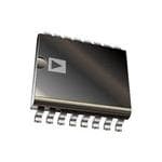
| 封装/箱体 | TSSOP-16 |
| 工作温度 | -40°C ~ 85°C |
| 工作电源电压 | 3 V |
| 工厂包装数量 | 1000 |
| 差分-输入:输出 | 是/无 |
| 最大工作温度 | + 85 C |
| 最大输入频率 | 400 MHz |
| 最小工作温度 | - 40 C |
| 最小输入频率 | 5 MHz |
| 标准包装 | 1 |
| 比率-输入:输出 | 2:1 |
| 电压-电源 | 2.7 V ~ 3.3 V |
| 电源电压-最大 | 3.3 V |
| 电源电压-最小 | 2.7 V |
| 电源电流 | 5 mA |
| 电路数 | 1 |
| 电路数量 | 1 |
| 类型 | Inter N |
| 系列 | ADF4002 |
| 输入 | CMOS,TTL |
| 输出 | 时钟 |
| 频率-最大值 | 400MHz |


- 商务部:美国ITC正式对集成电路等产品启动337调查
- 曝三星4nm工艺存在良率问题 高通将骁龙8 Gen1或转产台积电
- 太阳诱电将投资9.5亿元在常州建新厂生产MLCC 预计2023年完工
- 英特尔发布欧洲新工厂建设计划 深化IDM 2.0 战略
- 台积电先进制程称霸业界 有大客户加持明年业绩稳了
- 达到5530亿美元!SIA预计今年全球半导体销售额将创下新高
- 英特尔拟将自动驾驶子公司Mobileye上市 估值或超500亿美元
- 三星加码芯片和SET,合并消费电子和移动部门,撤换高东真等 CEO
- 三星电子宣布重大人事变动 还合并消费电子和移动部门
- 海关总署:前11个月进口集成电路产品价值2.52万亿元 增长14.8%


PDF Datasheet 数据手册内容提取
Phase Detector/Frequency Synthesizer Data Sheet ADF4002 FEATURES GENERAL DESCRIPTION 400 MHz bandwidth The ADF4002 frequency synthesizer is used to implement local 2.7 V to 3.3 V power supply oscillators in the upconversion and downconversion sections of Separate charge pump supply (VP) allows extended wireless receivers and transmitters. It consists of a low noise tuning voltage in 3 V systems digital phase frequency detector (PFD), a precision charge Programmable charge pump currents pump, a programmable reference divider, and programmable 3-wire serial interface N divider. The 14-bit reference counter (R counter) allows Analog and digital lock detect selectable REFIN frequencies at the PFD input. A complete Hardware and software power-down mode phase-locked loop (PLL) can be implemented if the synthesizer 104 MHz phase detector is used with an external loop filter and voltage controlled APPLICATIONS oscillator (VCO). In addition, by programming R and N to 1, the device can be used as a standalone PFD and charge pump. Clock conditioning Clock generation IF LO generation FUNCTIONAL BLOCK DIAGRAM AVDD DVDD VP CPGND RSET REFERENCE REFIN R C1O4U-BNITTER FREPQHAUSEENCY CHARGE CP PUMP DETECTOR 14 R COUNTER LOCK CURRENT CURRENT LATCH DETECT SETTING 1 SETTING 2 CLK 24-BIT INPUT FUNCTION DATA REGISTER 22 LATCH CPI3 CPI2 CPI1 CPI6 CPI5 CPI4 LE N COUNTER HIGH Z SDOUT LATCH AVDD MUXOUT MUX SDOUT RFINA 13-BIT RFINB N COUNTER M3 M2 M1 ADF4002 CE AGND DGND 06052-001 Figure 1. Rev. D Document Feedback Information furnished by Analog Devices is believed to be accurate and reliable. However, no responsibility is assumed by Analog Devices for its use, nor for any infringements of patents or other One Technology Way, P.O. Box 9106, Norwood, MA 02062-9106, U.S.A. rights of third parties that may result from its use. Specifications subject to change without notice. No license is granted by implication or otherwise under any patent or patent rights of Analog Devices. Tel: 781.329.4700 ©2006–2015 Analog Devices, Inc. All rights reserved. Trademarks and registered trademarks are the property of their respective owners. Technical Support www.analog.com
ADF4002 Data Sheet TABLE OF CONTENTS Features .............................................................................................. 1 MUXOUT and Lock Detect .........................................................9 Applications ....................................................................................... 1 Input Shift Register .......................................................................9 General Description ......................................................................... 1 Latch Maps and Descriptions ....................................................... 10 Functional Block Diagram .............................................................. 1 Latch Summary ........................................................................... 10 Revision History ............................................................................... 2 Reference Counter Latch Map .................................................. 11 Specifications ..................................................................................... 3 N Counter Latch Map ................................................................ 12 Timing Characteristics ................................................................ 4 Function Latch Map ................................................................... 13 Absolute Maximum Ratings ............................................................ 5 Initialization Latch Map ............................................................ 14 Thermal Characteristics .............................................................. 5 Function Latch ............................................................................ 15 ESD Caution .................................................................................. 5 Initialization Latch ..................................................................... 16 Pin Configurations and Function Descriptions ........................... 6 Applications ..................................................................................... 17 Typical Performance Characteristics ............................................. 7 Very Low Jitter Encode Clock for High Speed Converters ... 17 Theory of Operation ........................................................................ 8 PFD............................................................................................... 17 Reference Input Section ............................................................... 8 Interfacing ................................................................................... 17 RF Input Stage ............................................................................... 8 PCB Design Guidelines for Chip Scale Package .................... 18 N Counter ...................................................................................... 8 Outline Dimensions ....................................................................... 19 R Counter ...................................................................................... 8 Ordering Guide .......................................................................... 19 Phase Frequency Detector (PFD) and Charge Pump .............. 8 REVISION HISTORY 9/15—Rev. C to Rev. D 9/11—Rev. A to Rev. B Changed ADSP21xx to ADSP-2181 ............................ Throughout Changes to Normalized Phase Noise Floor (PN ) Parameter SYNTH Changes to Table 3 ............................................................................ 5 and Endnote 6, Table 1 ..................................................................... 4 Changes to Figure 4 .......................................................................... 6 Added Normalized 1/f Noise (PN ) Parameter and Endnote 7, 1_f Changes to Very Low Jitter Encode Clock for High Speed Table 1 ................................................................................................. 4 Converters Section and Figure 20 ................................................ 17 Changes to Figure 4 and Table 5 ...................................................... 6 Update Outline Dimensions ......................................................... 19 Updated Outline Dimensions ....................................................... 19 Changes to Ordering Guide .......................................................... 19 4/07—Rev. 0 to Rev. A 12/12—Rev. B to Rev. C Changes to Features List ................................................................... 1 Change to Table 1 ............................................................................. 4 Changes to Table 1 ............................................................................. 3 Added RF A to RF B Parameter, Table 3 .................................... 5 Deleted Figure .................................................................................... 7 IN IN Updated Outline Dimensions ....................................................... 19 Changes to Figure 16 ...................................................................... 11 Changes to Ordering Guide .......................................................... 19 4/06—Revision 0: Initial Version Rev. D | Page 2 of 20
Data Sheet ADF4002 SPECIFICATIONS AV = DV = 3 V ± 10%, AV ≤ V ≤ 5.5 V, AGND = DGND = CPGND = 0 V, R = 5.1 kΩ, dBm referred to 50 Ω, DD DD DD P SET T = T to T , unless otherwise noted. A MAX MIN Table 1. B Version1 Parameter Min Typ Max Unit Test Conditions/Comments RF CHARACTERISTICS See Figure 11 for input circuit RF Input Sensitivity −10 0 dBm RF Input Frequency (RF ) 5 400 MHz For RF < 5 MHz, ensure slew rate (SR) > 4 V/µs IN IN REFIN CHARACTERISTICS REFIN Input Frequency 20 300 MHz For REFIN < 20 MHz, ensure SR > 50 V/µs REFIN Input Sensitivity2 0.8 V V p-p Biased at AV /23 DD DD REFIN Input Capacitance 10 pF REFIN Input Current ±100 µA PHASE DETECTOR Phase Detector Frequency4 104 MHz ABP = 0, 0 (2.9 ns antibacklash pulse width) CHARGE PUMP Programmable, see Figure 18 I Sink/Source CP High Value 5 mA With R = 5.1 kΩ SET Low Value 625 µA Absolute Accuracy 2.5 % With R = 5.1 kΩ SET R Range 3.0 11 kΩ See Figure 18 SET I Three-State Leakage 1 nA T = 25°C CP A I vs. V 1.5 % 0.5 V ≤ V ≤ V − 0.5 V CP CP CP P Sink and Source Current Matching 2 % 0.5 V ≤ V ≤ V − 0.5 V CP P I vs. Temperature 2 % V = V/2 CP CP P LOGIC INPUTS V , Input High Voltage 1.4 V IH V , Input Low Voltage 0.6 V IL I , I , Input Current ±1 µA INH INL C , Input Capacitance 10 pF IN LOGIC OUTPUTS V , Output High Voltage 1.4 V Open-drain output chosen, 1 kΩ pull-up resistor to 1.8 V OH V , Output High Voltage V − 0.4 V CMOS output chosen OH DD I 100 µA OH V , Output Low Voltage 0.4 V I = 500 µA OL OL POWER SUPPLIES AV 2.7 3.3 V DD DV AV DD DD V AV 5.5 V AV ≤ V ≤ 5.5 V P DD DD P I 5 (AI + DI ) 5.0 6.0 mA DD DD DD I 0.4 mA T = 25°C P A Power-Down Mode 1 µA AI + DI DD DD Rev. D | Page 3 of 20
ADF4002 Data Sheet B Version1 Parameter Min Typ Max Unit Test Conditions/Comments NOISE CHARACTERISTICS Normalized Phase Noise Floor (PN )6 −222 dBc/Hz PLL loop bandwidth = 500 kHz, measured at 100 kHz offset SYNTH Normalized 1/f Noise (PN )7 −119 dBc/Hz 10 kHz offset; normalized to 1 GHz 1_f 1 Operating temperature range (B version) is −40°C to +85°C. 2 AVDD = DVDD = 3 V. 3 AC coupling ensures AVDD/2 bias. 4 Guaranteed by design. Sample tested to ensure compliance. 5 TA = 25°C; AVDD = DVDD = 3 V; RFIN = 350 MHz. The current for any other setup (25°C, 3.0 V) in mA is given by 2.35 + 0.0046 (REFIN) + 0.0062 (RF), RF frequency and REFIN frequency in MHz. 6 The synthesizer phase noise floor is estimated by measuring the in-band phase noise at the output of the VCO and subtracting 20 logN (where N is the N divider value) and 10 logFPFD. PNSYNTH = PNTOT – 10 logFPFD – 20 logN. 7 The PLL phase noise is composed of 1/f (flicker) noise plus the normalized PLL noise floor. The formula for calculating the 1/f noise contribution at an RF frequency, fRF, and at a frequency offset, f, is given by PN = PN1_f + 10 log(10 kHz/f) + 20 log(fRF/1 GHz). All phase noise measurements were performed with the EV-ADF4002SD1Z and the Agilent E5500 phase noise system. Both the normalized phase noise floor and flicker noise are modeled in ADIsimPLL. TIMING CHARACTERISTICS AV = DV = 3 V ± 10%, AV ≤ V ≤ 5.5 V, AGND = DGND = CPGND = 0 V, R = 5.1 kΩ, dBm referred to 50 Ω, T = T to T , DD DD DD P SET A MAX MIN unless otherwise noted.1 Table 2. Parameter Limit (B Version)2 Unit Test Conditions/Comments t 10 ns min DATA to CLK setup time 1 t 10 ns min DATA to CLK hold time 2 t 25 ns min CLK high duration 3 t 25 ns min CLK low duration 4 t 10 ns min CLK to LE setup time 5 t 20 ns min LE pulse width 6 1 Guaranteed by design, but not production tested. 2 Operating temperature range (B version) is −40°C to +85°C. Timing Diagram t3 t4 CLK t1 t2 DATA DB23 (MSB) DB22 DB2 DB1 B(CITO CN2T)ROL (CONDTBR0O (LLS BBIT) C1) t6 LE t5 LE 06052-022 Figure 2. Timing Diagram Rev. D | Page 4 of 20
Data Sheet ADF4002 ABSOLUTE MAXIMUM RATINGS T = 25°C, unless otherwise noted. This device is a high performance RF integrated circuit with an A ESD rating of <2 kV, and it is ESD sensitive. Take proper Table 3. precautions for handling and assembly. Parameter Rating AV to GND1 −0.3 V to +3.6 V DD AV to DV −0.3 V to +0.3 V THERMAL CHARACTERISTICS DD DD V to GND −0.3 V to +5.8 V P Table 4. Thermal Impedance V to AV −0.3 V to +5.8 V P DD Package Type θ Unit Digital I/O Voltage to GND −0.3 V to V + 0.3 V JA DD TSSOP 150.4 °C/W Analog I/O Voltage to GND −0.3 V to V + 0.3 V P LFCSP 122 °C/W REF , RF A, RF B to GND −0.3 V to V + 0.3 V IN IN IN DD RFINA to RFINB ±600 mV Operating Temperature Range ESD CAUTION Industrial (B Version) −40°C to +85°C Storage Temperature Range −65°C to +125°C Maximum Junction Temperature 150°C Reflow Soldering Peak Temperature (60 sec) 260°C Time at Peak Temperature 40 sec Transistor Count CMOS 6425 Bipolar 303 1 GND = AGND = DGND = 0 V. Stresses at or above those listed under Absolute Maximum Ratings may cause permanent damage to the product. This is a stress rating only; functional operation of the product at these or any other conditions above those indicated in the operational section of this specification is not implied. Operation beyond the maximum operating conditions for extended periods may affect product reliability. Rev. D | Page 5 of 20
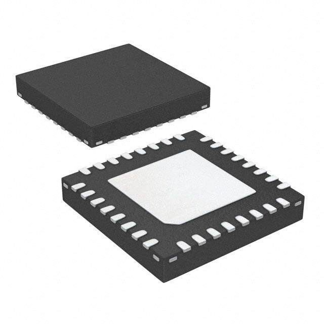
ADF4002 Data Sheet PIN CONFIGURATIONS AND FUNCTION DESCRIPTIONS P SET PVDDVDD CRVDD 09876 21111 CPGND 1 15 MUXOUT RSET 1 PININD I1CATOR 16 VP AGND 2 ADF4002 14 LE CP 2 15 DVDD AGND 3 TOP VIEW 13 DATA RFINB 4 (Not to Scale) 12 CLK CPGND 3 14 MUXOUT RFINA 5 11 CE AGND 4 ADF4002 13 LE RFINB 5 (NToOt Pto V SIEcWale)12 DATA 678901 D D NDD RFINA 6 11 CLK AVDAVDREFIDGNDGN RAEVFDIDN 78 190 CDEGND 06052-002 N1.O TTHEES EXPOSED PAD MUST BE CONNECTED TO AGND. 06052-003 Figure 3. TSSOP Pin Configuration (Top View) Figure 4. LFCSP Pin Configuration (Top View) Table 5. Pin Function Descriptions Pin No. TSSOP LFCSP Mnemonic Description 1 19 R Connecting a resistor between this pin and CPGND sets the maximum charge pump output current. The SET nominal voltage potential at the R pin is 0.66 V. The relationship between I and R is SET CP SET 25.5 I = CPMAX R SET where R = 5.1 kΩ and I = 5 mA. SET CP MAX 2 20 CP Charge Pump Output. When enabled, this provides ±I to the external loop filter that, in turn, drives the CP external VCO. 3 1 CPGND Charge Pump Ground. This is the ground return path for the charge pump. 4 2, 3 AGND Analog Ground. This is the ground return path of the RF input. 5 4 RF B Complementary Input to the RF Input. This point must be decoupled to the ground plane with a small IN bypass capacitor, typically 100 pF. See Figure 11. 6 5 RF A Input to the RF Input. This small signal input is ac-coupled to the external VCO. IN 7 6, 7 AV Analog Power Supply. This can range from 2.7 V to 3.3 V. Decoupling capacitors to the analog ground DD plane should be placed as close as possible to the AV pin. AV must be the same value as DV . DD DD DD 8 8 REF Reference Input. This is a CMOS input with a nominal threshold of V /2 and a dc equivalent input IN DD resistance of 100 kΩ. See Figure 10. This input can be driven from a TTL or CMOS crystal oscillator or it can be ac-coupled. 9 9, 10 DGND Digital Ground. 10 11 CE Chip Enable. A logic low on this pin powers down the device and puts the charge pump output into three- state mode. Taking this pin high powers up the device, depending on the status of the Power-Down Bit F2. 11 12 CLK Serial Clock Input. This serial clock is used to clock in the serial data to the registers. The data is latched into the 24-bit shift register on the CLK rising edge. This input is a high impedance CMOS input. 12 13 DATA Serial Data Input. The serial data is loaded MSB first with the two LSBs being the control bits. This input is a high impedance CMOS input. 13 14 LE Load Enable, CMOS Input. When LE goes high, the data stored in the shift registers is loaded into one of the four latches; the latch is selected using the control bits. 14 15 MUXOUT Multiplexer Output. This allows either the lock detect, the scaled RF, or the scaled reference frequency to be accessed externally. 15 16, 17 DV Digital Power Supply. This can range from 2.7 V to 3.3 V. Decoupling capacitors to the digital ground plane DD should be placed as close as possible to this pin. DV must be the same value as AV . DD DD 16 18 V Charge Pump Power Supply. This should be greater than or equal to V . In systems where V is 3 V, it can P DD DD be set to 5.5 V and used to drive a VCO with a tuning range of up to 5 V. EP Exposed Pad. The exposed pad must be connected to AGND. Rev. D | Page 6 of 20
Data Sheet ADF4002 TYPICAL PERFORMANCE CHARACTERISTICS 0 –130 –135 –5 –140 –10 Hz) WER (dBm) ––1250 +25°C NOISE (dBc/ –––111456550 O +85°C E P –25 S HA –165 P –30 –170 –40°C ––4305 06052-027 ––117850 06052-033 0 100 200 300 400 500 600 100k 1M 10M 100M 1G FREQUENCY (MHz) PFD FREQUENCY (Hz) Figure 5. RF Input Sensitivity Figure 8. Phase Noise (Referred to CP Output) vs. PFD Frequency 0 REF –4dBm MKR1 1.000 MHz SAMP LOG 10dB/ ATTN 10dB –94.5dBc 0 1R –10 –5 –40°C –20 m) +25°C –30 B –10 R (d –40 E W –50 O –15 +85°C P –60 –70 –20 –250 1 2 3 4 5 6 7 8 9 1006052-026 –1––098000 1 –94.5dBc 06052-030 FREQUENCY (MHz) CENTER 399.995MHz VBW 20kHz SPAN 2.2MHz RES BW 20kHz SWEEP 21ms (601pts) Figure 6. RF Input Sensitivity, Low Frequency Figure 9. Reference Spurs (400 MHz, 1 MHz, 7 kHz) –70 –80 rms NOISE = 0.07 DEGREES –90 Hz) c/ –100 B d E ( –110 S OI N –120 E S HA –130 P –140 ––115600 06052-031 1k 10k 100k 1M 10M FREQUENCY OFFSET (Hz) Figure 7. Integrated Phase Noise (400 MHz, 1 MHz, 50 kHz) Rev. D | Page 7 of 20
ADF4002 Data Sheet THEORY OF OPERATION REFERENCE INPUT SECTION The equation for the VCO frequency is The reference input stage is shown in Figure 10. SW1 and SW2 f f = N × REFIN are normally closed switches. SW3 is normally open. When VCO R power-down is initiated, SW3 is closed and SW1 and SW2 are where: opened. This ensures that there is no loading of the REF pin IN on power-down. fVCO is the output frequency of external voltage controlled oscillator (VCO). POWER-DOWN CONTROL N is the preset divide ratio of binary 13-bit counter (1 to 8191). f is the external reference frequency oscillator. REFIN FROM N NC 100kΩ COUNTER LATCH SW2 REFIN NC TO R COUNTER BUFFER SW1 NO SW3 06052-013 INPFURTO MST RAFGFiEgureC1 1O32U-B.N NITT ECNRounterT O PFD 06052-021 R COUNTER Figure 10. Reference Input Stage The 14-bit R counter allows the input reference frequency to be RF INPUT STAGE divided down to produce the reference clock to the phase The RF input stage is shown in Figure 11. It is followed by a frequency detector (PFD). Division ratios from 1 to 16,383 are 2-stage limiting amplifier to generate the CML clock levels allowed. needed for the N counter. PHASE FREQUENCY DETECTOR (PFD) AND CHARGE PUMP BIAS 1.6V GENERATOR AVDD The PFD takes inputs from the R counter and N counter and 500Ω 500Ω produces an output proportional to the phase and frequency difference between them. Figure 13 is a simplified schematic. The PFD includes a programmable delay element that controls RFINA the width of the antibacklash pulse. This pulse ensures that there is no dead zone in the PFD transfer function, and RFINB minimizes phase noise and reference spurs. Two bits in the reference counter latch (ABP2 and ABP1) control the width of AGND 06052-014 tphuel speu wlsied.t She ies Fniogtu rreec 1o6m fmore dnedteadil.s . The smallest antibacklash Figure 11. RF Input Stage VP CHARGE N COUNTER PUMP UP HI D1 Q1 The N CMOS counter allows a wide ranging division ratio in U1 the PLL feedback counter. Division ratios from 1 to 8191 are R DIVIDER CLR1 allowed. N and R Relationship PROGRAMMABLE DELAY U3 CP The N counter makes it possible to generate output frequencies that are spaced only by the reference frequency divided by R. ABP2 ABP1 CLR2 DOWN HI D2 Q2 N DIVIDER U2 CPGND 06052-023 Figure 13. PFD Simplified Schematic and Timing (In Lock) Rev. D | Page 8 of 20
Data Sheet ADF4002 MUXOUT AND LOCK DETECT analog lock detect is more accurate because of the smaller pulse widths. The output multiplexer on the ADF4002 allows the user to access various internal points on the chip. The state of The N-channel, open-drain, analog lock detect should be MUXOUT is controlled by M3, M2, and M1 in the function operated with an external pull-up resistor of 10 kΩ nominal. latch. Figure 18 shows the full truth table. Figure 14 shows the When lock has been detected, this output is high with narrow, MUXOUT section in block diagram form. low going pulses. DVDD INPUT SHIFT REGISTER The ADF4002 digital section includes a 24-bit input shift ANALOG LOCK DETECT register, a 14-bit R counter, and a 13-bit N counter. Data is clocked into the 24-bit shift register on each rising edge of CLK. DIGITAL LOCK DETECT The data is clocked in MSB first. Data is transferred from the R COUNTER OUTPUT MUX CONTROL MUXOUT shift register to one of four latches on the rising edge of LE. The N COUNTER OUTPUT destination latch is determined by the state of the two control SDOUT bits (C2, C1) in the shift register. These are the two LSBs, DB1 and DB0, as shown in the timing diagram (see Figure 2). Table 6 DGND 06052-024 psuromvmidaersy t hoef htrouwth t htaeb llaet cfohre st haersee p broitgs.r aFmigmureed 1. 5 shows a Figure 14. MUXOUT Circuit Table 6. C2, C1 Truth Table Lock Detect Control Bits MUXOUT can be programmed for two types of lock detect: C2 C1 Data Latch digital lock detect and analog lock detect. 0 0 R Counter Digital lock detect is active high. When LDP in the R counter 0 1 N Counter latch is set to 0, digital lock detect is set high when the phase 1 0 Function Latch error on three consecutive phase detector (PD) cycles is less 1 1 Initialization Latch than 15 ns. With LDP set to 1, five consecutive cycles of less than 15 ns are required to set the lock detect. It stays set at high until a phase error of greater than 25 ns is detected on any subsequent PD cycle. For PFD frequencies greater than 10 MHz, Rev. D | Page 9 of 20
ADF4002 Data Sheet LATCH MAPS AND DESCRIPTIONS LATCH SUMMARY REFERENCE COUNTER LATCH N TO RESERVED LOCKDETECRECISIMOTDEES BTITS BAWCAKINDLTTAIH-SH 14-BIT REFERENCE COUNTER COBNITTRSOL P DB23 DB22 DB21 DB20 DB19 DB18 DB17 DB16 DB15 DB14 DB13 DB12 DB11 DB10 DB9 DB8 DB7 DB6 DB5 DB4 DB3 DB2 DB1 DB0 X 0 0 LDP T2 T1 ABP2 ABP1 R14 R13 R12 R11 R10 R9 R8 R7 R6 R5 R4 R3 R2 R1 C2 (0) C1 (0) N COUNTER LATCH N RESERVED GAI 13-BIT N COUNTER RESERVED CONTROL P BITS C DB23 DB22 DB21 DB20 DB19 DB18 DB17 DB16 DB15 DB14 DB13 DB12 DB11 DB10 DB9 DB8 DB7 DB6 DB5 DB4 DB3 DB2 DB1 DB0 X X G1 B13 B12 B11 B10 B9 B8 B7 B6 B5 B4 B3 B2 B1 X X X X X X C2 (0) C1 (1) FUNCTION LATCH RESERVED POWER-DOWN 2 CSUERTR2TEINNGT CSUERTR1TEINNGT TIMECRO NCTORUONLTER FASTLOCKMODE FASTLOCKENABLE CP THREE-STATE PDPOLARITY CMOUNXTORUOTL POWER-DOWN 1 COUNTERRESET COBNITTRSOL DB23 DB22 DB21 DB20 DB19 DB18 DB17 DB16 DB15 DB14 DB13 DB12 DB11 DB10 DB9 DB8 DB7 DB6 DB5 DB4 DB3 DB2 DB1 DB0 X X PD2 CPI6 CPI5 CPI4 CPI3 CPI2 CPI1 TC4 TC3 TC2 TC1 F5 F4 F3 F2 M3 M2 M1 PD1 F1 C2 (1) C1 (0) INITIALIZATION LATCH RESERVED POWER-DOWN 2 CSUERTR2TEINNGT CSUERTR1TEINNGT TIMECRO NCTORUONLTER FASTLOCKMODE FASTLOCKENABLE CP THREE-STATE PDPOLARITY CMOUNXTORUOTL POWER-DOWN 1 COUNTERRESET COBNITTRSOL DB23 DB22 DB21 DB20 DB19 DB18 DB17 DB16 DB15 DB14 DB13 DB12 DB11 DB10 DB9 DB8 DB7 DB6 DB5 DB4 DB3 DB2 DB1 DB0 X X PD2 CPI6 CPI5 CPI4 CPI3 CPI2 CPI1 TC4 TC3 TC2 TC1 F5 F4 F3 F2 M3 M2 M1 PD1 F1 C2 (1) C1 (1) 06052-015 Figure 15. Latch Summary Rev. D | Page 10 of 20
Data Sheet ADF4002 REFERENCE COUNTER LATCH MAP N RESERVED LOCKDETECTRECISIO MOTDEES BTITS BAWCAKINDLTTAIH-SH 14-BIT REFERENCE COUNTER COBNITTRSOL P DB23 DB22 DB21 DB20 DB19 DB18 DB17 DB16 DB15 DB14 DB13 DB12 DB11 DB10 DB9 DB8 DB7 DB6 DB5 DB4 DB3 DB2 DB1 DB0 X 0 0 LDP T2 T1 ABP2 ABP1 R14 R13 R12 R11 R10 R9 R8 R7 R6 R5 R4 R3 R2 R1 C2 (0) C1 (0) X = DON’T CARE R14 R13 R12 .......... R3 R2 R1 DIVIDE RATIO 0 0 0 .......... 0 0 1 1 0 0 0 .......... 0 1 0 2 0 0 0 .......... 0 1 1 3 0 0 0 .......... 1 0 0 4 . . . .......... . . . . . . . .......... . . . . . . . .......... . . . . 1 1 1 .......... 1 0 0 16380 1 1 1 .......... 1 0 1 16381 1 1 1 .......... 1 1 0 16382 1 1 1 .......... 1 1 1 16383 ABP2 ABP1 ANTIBACKLASH PULSE WIDTH 0 0 2.9ns 0 1 NOT ALLOWED 1 0 6.0ns 1 1 2.9ns TEST MODE BITS SHOULD BE SET TO 00 FOR NORMAL OPERATION. LDP OPERATION 0 THREE CONSECUTIVE CYCLES OF PHASE DELAY LESS THAN 15ns MUST OCCUR BEFORE LOCK DETECT IS SET. 1 FIVE CONSECUTIVE CYCLES OF PHASE DELAY LESS THAN 15ns MUST OCCUR BEFORE LOCK DETECT IS SET. BMNOOUTRSHTM AOBLEF OSTPEHETERSTAEOT B0IOI TFNSO.R 06052-025 Figure 16. Reference Counter Latch Map Rev. D | Page 11 of 20
ADF4002 Data Sheet N COUNTER LATCH MAP N RESERVED P GAI 13-BIT N COUNTER RESERVED COBNITTRSOL C DB23 DB22 DB21 DB20 DB19 DB18 DB17 DB16 DB15 DB14 DB13 DB12 DB11 DB10 DB9 DB8 DB7 DB6 DB5 DB4 DB3 DB2 DB1 DB0 X X G1 B13 B12 B11 B10 B9 B8 B7 B6 B5 B4 B3 B2 B1 X X X X X X C2 (0) C1 (1) X = DON’T CARE N13 N12 N11 N3 N2 N1 N COUNTER DIVIDE RATIO 0 0 0 .......... 0 0 0 NOTALLOWED 0 0 0 .......... 0 0 1 1 0 0 0 .......... 0 1 0 2 0 0 0 .......... 0 1 1 3 . . . .......... . . . . . . . .......... . . . . . . . .......... . . . . 1 1 1 .......... 1 0 0 8188 1 1 1 .......... 1 0 1 8189 1 1 1 .......... 1 1 0 8190 1 1 1 .......... 1 1 1 8191 F4 (FUNCTION LATCH) FASTLOCK ENABLE CP GAIN OPERATION 0 0 CHARGE PUMP CURRENT SETTING 1 IS PERMANENTLY USED. 0 1 CHARGE PUMP CURRENT SETTING 2 IS PERMANENTLY USED. 1 0 CHARGE PUMP CURRENT SETTING 1 IS USED. 1 1 CHARGE PUMP CURRENT IS SWITCHEDTO SETTING 2. THE TIME SPENT IN SETTING 2 IS DEPENDENT ON WHICHFASTLOCK MODE IS USED. SEE FUNCTION THESE BITSARE NOT USED LATCH DESCRIPTION. BY THE DEVICEANDARE DON'T CARE BITS. THESE BITSARE NOT USED BDOY NT'HTE C DAERVEI CBEITASN.DARE 06052-016 Figure 17. N Counter Latch Map Rev. D | Page 12 of 20
Data Sheet ADF4002 FUNCTION LATCH MAP RESERVED POWER-DOWN 2 CSUERTR2TEINNGT CSUERTR1TEINNGT TIMECRO NCTORUONLTER FASTLOCKMODE FASTLOCKENABLE CP THREE-STATE PDPOLARITY CMOUNXTORUOTL POWER-DOWN 1 COUNTERRESET COBNITTRSOL DB23 DB22 DB21 DB20 DB19 DB18 DB17 DB16 DB15 DB14 DB13 DB12 DB11 DB10 DB9 DB8 DB7 DB6 DB5 DB4 DB3 DB2 DB1 DB0 X X PD2 CPI6 CPI5 CPI4 CPI3 CPI2 CPI1 TC4 TC3 TC2 TC1 F5 F4 F3 F2 M3 M2 M1 PD1 F1 C2 (1) C1 (0) PHASE DETECTOR COUNTER F2 POLARITY F1 OPERATION 0 NEGATIVE 0 NORMAL 1 POSITIVE 1 R COUNTERAND N COUNTER HELD IN RESET CHARGE PUMP F3 OUTPUT 0 NORMAL 1 THREE-STATE F4 F5 FASTLOCK MODE 0 X FASTLOCK DISABLED 1 0 FASTLOCK MODE 1 1 1 FASTLOCK MODE 2 M3 M2 M1 OUTPUT TIMEOUT TC4 TC3 TC2 TC1 (PFD CYCLES) 0 0 0 THREE-STATE OUTPUT 0 0 0 0 3 0 0 1 DIGITAL LOCK DETECT (ACTIVE HIGH) 0 0 0 1 7 0 1 0 N DIVIDER OUTPUT 0 0 1 0 11 0 0 1 1 15 0 1 1 DVDD 1 0 0 R DIVIDER OUTPUT 0 1 0 0 19 1 0 1 N-CHANNEL OPEN-DRAIN 0 1 0 1 23 LOCK DETECT 0 1 1 0 27 1 1 0 SERIAL DATA OUTPUT 0 1 1 1 31 1 1 1 DGND 1 0 0 0 35 1 0 0 1 39 1 0 1 0 43 1 0 1 1 47 1 1 0 0 51 1 1 0 1 55 1 1 1 0 59 1 1 1 1 63 SEEPAGE 15 CPI6 CPI5 CP14 ICP (mA) CPI3 CPI2 CPI1 3kΩ 5.1kΩ 11kΩ 0 0 0 1.088 0.625 0.294 0 0 1 2.176 1.250 0.588 0 1 0 3.264 1.875 0.882 0 1 1 4.352 2.500 1.176 1 0 0 5.440 3.125 1.470 1 0 1 6.528 3.750 1.764 1 1 0 7.616 4.375 2.058 1 1 1 8.704 5.000 2.352 CE PIN PD2 PD1 MODE 0 X X ASYNCHRONOUS POWER-DOWN 1 X 0 NORMAL OPERATION 1 0 1 ASYNCHRONOUS POWER-DOWN 1 1 1 SYNCHRONOUS POWER-DOWN THESE BITSARE NOT USED BY THE DEVICEANDARE DON'T CARE BITS. 06052-017 Figure 18. Function Latch Map Rev. D | Page 13 of 20
ADF4002 Data Sheet INITIALIZATION LATCH MAP RESERVED POWER-DOWN 2 CSUERTR2TEINNGT CSUERTR1TEINNGT TIMECRO NCTORUONLTER FASTLOCKMODE FASTLOCKENABLE CP THREE-STATE PDPOLARITY CMOUNXTORUOTL POWER-DOWN 1 COUNTERRESET COBNITTRSOL DB23 DB22 DB21 DB20 DB19 DB18 DB17 DB16 DB15 DB14 DB13 DB12 DB11 DB10 DB9 DB8 DB7 DB6 DB5 DB4 DB3 DB2 DB1 DB0 X X PD2 CPI6 CPI5 CPI4 CPI3 CPI2 CPI1 TC4 TC3 TC2 TC1 F5 F4 F3 F2 M3 M2 M1 PD1 F1 C2 (1) C1 (1) PHASE DETECTOR COUNTER F2 POLARITY F1 OPERATION 0 NEGATIVE 0 NORMAL 1 POSITIVE 1 R COUNTERAND N COUNTER HELD IN RESET CHARGE PUMP F3 OUTPUT 0 NORMAL 1 THREE-STATE F4 F5 FASTLOCK MODE 0 X FASTLOCK DISABLED 1 0 FASTLOCK MODE 1 1 1 FASTLOCK MODE 2 M3 M2 M1 OUTPUT TIMEOUT TC4 TC3 TC2 TC1 (PFD CYCLES) 0 0 0 THREE-STATE OUTPUT 0 0 0 0 3 0 0 1 DIGITAL LOCK DETECT 0 0 0 1 7 (ACTIVE HIGH) 0 1 0 N DIVIDER OUTPUT 0 0 1 0 11 0 0 1 1 15 0 1 1 DVDD 1 0 0 R DIVIDER OUTPUT 0 1 0 0 19 1 0 1 N-CHANNEL OPEN-DRAIN 0 1 0 1 23 LOCK DETECT 0 1 1 0 27 1 1 0 SERIAL DATA OUTPUT 0 1 1 1 31 1 1 1 DGND 1 0 0 0 35 1 0 0 1 39 1 0 1 0 43 1 0 1 1 47 1 1 0 0 51 1 1 0 1 55 1 1 1 0 59 1 1 1 1 63 SEEPAGE 16 CPI6 CPI5 CP14 ICP (mA) CPI3 CPI2 CPI1 3kΩ 5.1kΩ 11kΩ 0 0 0 1.088 0.625 0.294 0 0 1 2.176 1.250 0.588 0 1 0 3.264 1.875 0.882 0 1 1 4.352 2.500 1.176 1 0 0 5.440 3.125 1.470 1 0 1 6.528 3.750 1.764 1 1 0 7.616 4.375 2.058 1 1 1 8.704 5.000 2.352 CE PIN PD2 PD1 MODE 0 X X ASYNCHRONOUS POWER-DOWN 1 X 0 NORMAL OPERATION 1 0 1 ASYNCHRONOUS POWER-DOWN 1 1 1 SYNCHRONOUS POWER-DOWN THESE BITSARE NOT USED BY THE DEVICEANDARE DON'T CARE BITS. Figure 19. Initialization Latch Map 06052-036 Rev. D | Page 14 of 20
Data Sheet ADF4002 FUNCTION LATCH Fastlock Mode Bit With C2, C1 set to 1, 0, the on-chip function latch is DB10 of the function latch is the fastlock mode bit. When programmed. Figure 18 shows the input data format for fastlock is enabled, this bit determines the fastlock mode to be programming the function latch. used. If the fastlock mode bit is 0, then Fastlock Mode 1 is selected, and if the fastlock mode bit is 1, then Fastlock Mode 2 Counter Reset is selected. DB2 (F1) is the counter reset bit. When this bit is set to 1, the Fastlock Mode 1 R counter and the N counter are reset. For normal operation, set this bit to 0. Upon powering up, the F1 bit needs to be In this mode, the charge pump current is switched to the disabled (set to 0). Then, the N counter resumes counting in contents of Current Setting 2. The device enters fastlock by close alignment with the R counter (the maximum error is one having a 1 written to the CP gain bit in the N counter latch. The prescaler cycle). device exits fastlock by having a 0 written to the CP gain bit in the AB counter latch. Power-Down Fastlock Mode 2 DB3 (PD1) and DB21 (PD2) provide programmable power- down modes. These bits are enabled by the CE pin. In this mode, the charge pump current is switched to the contents of Current Setting 2. The device enters fastlock by When the CE pin is low, the device is immediately disabled having a 1 written to the CP gain bit in the N counter latch. The regardless of the states of the PD2, PD1 bits. device exits fastlock under the control of the timer counter. In the programmed asynchronous power-down, the device After the timeout period determined by the value in TC4 to powers down immediately after latching a 1 into Bit PD1, with TC1, the CP gain bit in the N counter latch is automatically the condition that Bit PD2 has been loaded with a 0. reset to 0 and the device reverts to normal mode instead of In the programmed synchronous power-down, the device fastlock. See Figure 18 for the timeout periods. power-down is gated by the charge pump to prevent unwanted Timer Counter Control frequency jumps. Once the power-down is enabled by writing The user has the option of programming two charge pump a 1 into Bit PD1 (on condition that a 1 has also been loaded to currents. The intent is to use the Current Setting 1 when the Bit PD2), then the device enters power-down on the occurrence RF output is stable and the system is in a static state. Current of the next charge pump event. Setting 2 is meant to be used when the system is dynamic and When a power-down is activated (either in synchronous or in a state of change, that is, when a new output frequency is asynchronous mode, including a CE pin activated power- programmed. down), the following events occur: The normal sequence of events is as follows: • All active dc current paths are removed. The user initially decides the referred charge pump currents. • The R, N, and timeout counters are forced to their load For example, the choice can be 2.5 mA as Current Setting 1 and state conditions. 5 mA as Current Setting 2. • The charge pump is forced into three-state mode. At the same time, the decision must be made as to how long the • The digital lock detect circuitry is reset. secondary current is to stay active before reverting to the • The RFIN input is debiased. primary current. This is controlled by Timer Counter Control • The reference input buffer circuitry is disabled. Bit DB14 to Timer Counter Control Bit DB11 (TC4 to TC1) in • The input register remains active and capable of loading the function latch. See Figure 18 for the truth table. and latching data. To program a new output frequency, simply program the N MUXOUT Control counter latch with a new value for N. At the same time, the CP The on-chip multiplexer is controlled by M3, M2, and M1 on gain bit can be set to 1. This sets the charge pump with the the ADF4002. Figure 18 shows the truth table. value in CPI6 to CPI4 for a period of time determined by TC4 to TC1. When this time is up, the charge pump current reverts Fastlock Enable Bit to the value set by CPI3 to CPI1. At the same time, the CP gain DB9 of the function latch is the fastlock enable bit. Only when bit in the N counter latch is reset to 0 and is ready for the next this is 1 is fastlock enabled. time that the user wishes to change the frequency. Note that there is an enable feature on the timer counter. It is enabled when Fastlock Mode 2 is chosen by setting the Fastlock Mode Bit DB10 in the function latch to 1. Rev. D | Page 15 of 20
ADF4002 Data Sheet Charge Pump Currents When the initialization latch is loaded, the following occurs: CPI3, CPI2, and CPI1 program Current Setting 1 for the charge • The function latch contents are loaded. pump. CPI6, CPI5, and CPI4 program Current Setting 2 for the • An internal pulse resets the R, N, and timeout counters to charge pump. See Figure 18 for the truth table. load state conditions and three-states the charge pump. PD Polarity Note that the prescaler band gap reference and the oscilla- tor input buffer are unaffected by the internal reset pulse, This bit sets the phase detector polarity bit (see Figure 18). allowing close phase alignment when counting resumes. CP Three-State • Latching the first N counter data after the initialization This bit controls the CP output pin. Setting the bit high puts the word activates the same internal reset pulse. Successive N CP output into three-state. With the bit set low, the CP output loads do not trigger the internal reset pulse unless there is is enabled. another initialization. INITIALIZATION LATCH CE Pin Method The initialization latch is programmed when C2, C1 = 1, 1. This 1. Apply V . DD is essentially the same as the function latch (programmed when 2. Bring CE low to put the device into power-down. This is an C2, C1 = 1, 0). asynchronous power-down because it happens immediately. However, when the initialization latch is programmed there is 3. Program the function latch (10). an additional internal reset pulse applied to the R and N 4. Program the R counter latch (00). counters. This pulse ensures that the N counter is at load point 5. Program the N counter latch (01). when the N counter data is latched and the device begins 6. Bring CE high to take the device out of power-down. The counting in close phase alignment. R and N counters resume counting in close alignment. Note that after CE goes high, a duration of 1 µs can be If the latch is programmed for synchronous power-down (CE required for the prescaler band gap voltage and oscillator pin is high; PD1 bit is high; and PD2 bit is low), the internal input buffer bias to reach steady state. pulse also triggers this power-down. The prescaler reference and the oscillator input buffer are unaffected by the internal CE can be used to power the device up and down to check for reset pulse, thereby maintaining close phase alignment when channel activity. The input register does not need to be counting resumes. reprogrammed each time the device is disabled and enabled, as When the first N counter data is latched after initialization, the long as it has been programmed at least once after VDD was internal reset pulse is reactivated. However, successive AB initially applied. counter loads after this do not trigger the internal reset pulse. Counter Reset Method Device Programming After Initial Power-Up 1. Apply V . DD After initially powering up the device, there are three ways to 2. Do a function latch load (10 in two LSBs). As part of this program the device. step, load 1 to the F1 bit. This enables the counter reset. 3. Perform an R counter load (00 in two LSBs). Initialization Latch Method 4. Perform an N counter load (01 in two LSBs). 1. Apply VDD. 5. Do a function latch load (10 in two LSBs). As part of this 2. Program the initialization latch (11 in two LSBs of input step, load 0 to the F1 bit. This disables the counter reset. word). Make sure that the F1 bit is programmed to 0. This sequence provides the same close alignment as the 3. Conduct a function latch load (10 in two LSBs of the initialization method. It offers direct control over the internal control word). Make sure that the F1 bit is programmed to 0. reset. Note that counter reset holds the counters at load point 4. Perform an R load (00 in two LSBs). and three-states the charge pump, but does not trigger 5. Perform an N load (01 in two LSBs). synchronous power-down. Rev. D | Page 16 of 20
Data Sheet ADF4002 APPLICATIONS INFORMATION VERY LOW JITTER ENCODE CLOCK FOR HIGH PFD SPEED CONVERTERS As the ADF4002 permits both R and N counters to be pro- Figure 20 shows the ADF4002 with a VCXO to provide the grammed to 1, the part can effectively be used as a standalone encode clock for a high speed analog-to-digital converter (ADC). PFD and charge pump. This is particularly useful in either a clock cleaning application or a high performance LO. Addi- The converter used in this application is an AD9215-80, a 12-bit tionally, the very low normalized phase noise floor (−222 dBc/Hz) converter that accepts up to an 80 MHz encode clock. To realize enables very low in-band phase noise levels. It is possible to a stable low jitter clock, use a 77.76 MHz, narrow-band VCXO. operate the PFD up to a maximum frequency of 104 MHz. This example assumes a 19.44 MHz reference clock. In Figure 21, the reference frequency equals the PFD; therefore, To minimize the phase noise contribution of the ADF4002, the R = 1. The charge pump output integrates into a stable control smallest multiplication factor of 4 is used. Thus, the R divider is voltage for the VCXO, and the output from the VCXO is divided programmed to 1, and the N divider is programmed to 4. down to the desired PFD frequency using an external divider. The charge pump output of the ADF4002 (Pin 2) drives the loop filter. The loop filter bandwidth is optimized for the best VDD VP RFOUT possible rms jitter, a key factor in the signal-to-noise ratio 100pF (SNR) of the ADC. Too narrow a bandwidth allows the VCXO 7 15 16 2 LOOP VCC VCO 100pF 18Ω 18Ω noise to dominate at small offsets from the carrier frequency. VDD VDD VPCE FILTER VOCXRO Too wide a bandwidth allows the ADF4002 noise to dominate at REFIN 8 AREFDIN RSET 1 GND 18Ω offsets where the VCXO noise is lower than the ADF4002 noise. 10kΩ VCC ADF4002 Thus, the intersection of the VCXO noise and the ADF4002 in- 100pF VCC band noise is chosen as the optimum loop filter bandwidth. ND D D RFINA 6 EXTERNAL PRESCALER The design of the loop filter uses the ADIsimPLL (Version 3.0) and CPG AGN DGN RFINB 5 51Ω GND iTs haev arimlabs ljei tatse ra ifsr eme edaoswurneloda adt f<ro1m.2 pwsw. Twh.ainsa lleovge.cl oism lo/AwDerI stihmaPnL L. 3 4 9 10DI0NpETFCEORUFPALCIEN GS ICGANPAALCSI THOARVES BAENEDN 06052-035 OMITTED FROM THE DIAGRAM IN the maximum allowable 6 ps rms required to ensure the THE INTERESTS OF GREATER CLARITY. theoretical SNR performance of 59 dB for this converter. Figure 21. ADF4002 as a PFD The setup shown in Figure 20 using the ADF4002, AD9215, and INTERFACING an ADC FIFO evaluation board allows the user to quickly and The ADF4002 has a simple SPI-compatible serial interface for effectively determine the suitability of the converter and encode writing to the device. CLK, DATA, and LE control the data clock. The SPI® interface is used to control the ADF4002, and the transfer. When the latch enable (Pin LE) goes high, the 24 bits USB interface helps control the operation of the AD9215-80. The that have been clocked into the input register on each rising controller board sends back FFT information to the PC that, if edge of CLK are transferred to the appropriate latch. For more using an ADC analyzer, provides all conversion results from the information, see Figure 2 for the timing diagram and Table 6 for ADC. the latch truth table. SPI The maximum allowable serial clock rate is 20 MHz. This TCXO: VCXO: 77.76MHz 19.44MHz ADF4002 means that the maximum update rate possible for the device is R = 1 PC 833 kHz, or one update every 1.2 μs. This is certainly more than PD N = 4 adequate for systems that have typical lock times in hundreds of microseconds. B S U ENCODE CLOCK ADC FIFO 500AkHGzIL, 1E.N8VT: p-p AIN AD9215-80 EVABLOUAARTDION 06052-034 Figure 20. ADF4002 as Encode Clock Rev. D | Page 17 of 20
ADF4002 Data Sheet ADuC812 Interface interrupt is generated. Set up the word length for eight bits and use three memory locations for each 24-bit word. To program Figure 22 shows the interface between the ADF4002 and the each 24-bit latch, store the three 8-bit bytes, enable the ADuC812 MicroConverter®. Because the ADuC812 is based on autobuffered mode, and then write to the transmit register of an 8051 core, this interface can be used with any 8051-based the DSP. This last operation initiates the autobuffer transfer. microcontroller. The MicroConverter is set up for SPI master mode with CPHA = 0. To initiate the operation, the I/O port SCLK CLK driving LE is brought low. Each latch of the ADF4002 needs a 24-bit word. This is accomplished by writing three 8-bit bytes DT DATA ADSP-2181 ADF4002 from the MicroConverter to the device. When the third byte TFS LE has been written, bring the LE input high to complete the CE transfer. On first applying power to the ADF4002, it needs four writes I/O FLAGS M(LUOXCOKU DTETECT) 06052-020 (one each to the initialization latch, function latch, R counter Figure 23. ADSP-2181 to ADF4002 Interface latch, and N counter latch) for the output to become active. PCB DESIGN GUIDELINES FOR CHIP SCALE I/O port lines on the ADuC812 are also used to control power- PACKAGE down (CE input) and to detect lock (MUXOUT configured as The lands on the lead frame chip scale package (CP-20-1) are lock detect and polled by the port input). rectangular. The printed circuit board pad for these should be When operating in the SPI master mode, the maximum SCLOCK 0.1 mm longer than the package land length and 0.05 mm wider rate of the ADuC812 is 4 MHz. This means that the maximum than the package land width. The land should be centered on rate at which the output frequency can be changed is 166 kHz. the pad. This ensures that the solder joint size is maximized. The bottom of the lead frame chip scale package has a central SCLOCK CLK thermal pad. MOSI DATA ADuC812 ADF4002 The thermal pad on the printed circuit board should be at least LE as large as this exposed pad. On the printed circuit board, there I/O PORTS CE should be a clearance of at least 0.25 mm between the thermal M(LUOXCOKU DTETECT) 06052-019 pshaodr atinndg tihs ea vinonideerd e.d ges of the pad pattern. This ensures that Figure 22. ADuC812 to ADF4002 Interface Thermal vias can be used on the printed circuit board thermal ADSP-2181 Interface pad to improve thermal performance of the package. If vias are used, they should be incorporated into the thermal pad at a Figure 23 shows the interface between the ADF4002 and the 1.2 mm pitch grid. The via diameter should be between 0.3 mm ADSP-2181 digital signal processor. The ADF4002 needs a and 0.33 mm and the via barrel should be plated with 1 oz 24-bit serial word for each latch write. The easiest way to accom- copper to plug the via. plish this using the ADSP-2181 family is to use the autobuffered transmit mode of operation with alternate framing. This provides The user should connect the printed circuit board thermal pad a means for transmitting an entire block of serial data before an to AGND. Rev. D | Page 18 of 20
Data Sheet ADF4002 OUTLINE DIMENSIONS 5.10 5.00 4.90 16 9 4.50 6.40 4.40 BSC 4.30 1 8 PIN 1 1.20 MAX 0.15 0.20 0.05 0.09 0.75 0.30 8° 0.60 0.65 0.19 SEATING 0° 0.45 BSC PLANE COPLANARITY 0.10 COMPLIANT TO JEDEC STANDARDS MO-153-AB Figure 24. 16-Lead Thin Shrink Small Outline Package [TSSOP] (RU-16) Dimensions shown in millimeters 4.10 0.30 4.00SQ 0.25 PIN1 3.90 0.18 INDICATOR PIN1 16 20 INDICATOR 0.50 BSC 15 1 EXPOSED 2.30 PAD 2.10SQ 2.00 11 5 0.65 10 6 0.20MIN TOPVIEW 0.60 BOTTOMVIEW 0.55 0.80 FORPROPERCONNECTIONOF 0.75 THEEXPOSEDPAD,REFERTO 0.05MAX THEPINCONFIGURATIONAND 0.70 0.02NOM FUNCTIONDESCRIPTIONS SECTIONOFTHISDATASHEET. COPLANARITY SEATING 0.08 PLANE COMPLIANTTOJED0E.2C0SRTEAFNDARDSMO-220-WGGD-1. 08-16-2010-B Figure 25. 20-Lead Lead Frame Chip Scale Package [LFCSP] 4 mm × 4 mm Body, and 0.75 mm Package Height (CP-20-6) Dimensions shown in millimeters ORDERING GUIDE Model1 Temperature Range Package Description Package Option ADF4002BRUZ −40°C to +85°C 16-Lead TSSOP RU-16 ADF4002BRUZ-RL −40°C to +85°C 16-Lead TSSOP RU-16 ADF4002BRUZ-RL7 −40°C to +85°C 16-Lead TSSOP RU-16 ADF4002BCPZ −40°C to +85°C 20-Lead LFCSP CP-20-6 ADF4002BCPZ-RL −40°C to +85°C 20-Lead LFCSP CP-20-6 ADF4002BCPZ-RL7 −40°C to +85°C 20-Lead LFCSP CP-20-6 EV-ADF4002SD1Z Evaluation Board EV-ADF411XSD1Z Evaluation Board 1 Z = RoHS Compliant Part. Rev. D | Page 19 of 20
ADF4002 Data Sheet NOTES ©2006–2015 Analog Devices, Inc. All rights reserved. Trademarks and registered trademarks are the property of their respective owners. D06052-0-9/15(D) Rev. D | Page 20 of 20
Mouser Electronics Authorized Distributor Click to View Pricing, Inventory, Delivery & Lifecycle Information: A nalog Devices Inc.: EV-ADF4002SD1Z ADF4002BRUZ ADF4002SRU-EP-RL7 ADF4002BCPZ-RL7 ADF4002BRUZ-RL7 ADF4002SRU-EP ADF4002BRUZ-RL ADF4002BCPZ ADF4002BCPZ-RL ADF4002SRUZ-EP ADF4002SRUZ-EP- RL7