ICGOO在线商城 > 集成电路(IC) > 线性 - 放大器 - 仪表,运算放大器,缓冲器放大器 > ADA4661-2ARMZ
 Datasheet下载
- 型号: ADA4661-2ARMZ
- 制造商: Analog
- 库位|库存: xxxx|xxxx
- 要求:
| 数量阶梯 | 香港交货 | 国内含税 |
| +xxxx | $xxxx | ¥xxxx |
查看当月历史价格
查看今年历史价格
ADA4661-2ARMZ产品简介:
ICGOO电子元器件商城为您提供ADA4661-2ARMZ由Analog设计生产,在icgoo商城现货销售,并且可以通过原厂、代理商等渠道进行代购。 ADA4661-2ARMZ价格参考。AnalogADA4661-2ARMZ封装/规格:线性 - 放大器 - 仪表,运算放大器,缓冲器放大器, 通用 放大器 2 电路 满摆幅 8-MSOP。您可以下载ADA4661-2ARMZ参考资料、Datasheet数据手册功能说明书,资料中有ADA4661-2ARMZ 详细功能的应用电路图电压和使用方法及教程。
ADA4661-2ARMZ 是由 Analog Devices Inc. 生产的一款双通道低噪声、高精度仪表放大器,属于线性 - 放大器 - 仪表/运算放大器/缓冲器放大器类别。其应用场景广泛,特别是在需要高精度信号调理和低噪声性能的领域中表现优异。以下是该型号的主要应用场景:

 1. 医疗设备
   - 心电图(ECG)和脑电图(EEG):ADA4661-2ARMZ 的低噪声特性和高共模抑制比(CMRR)使其非常适合用于放大微弱的生物电信号。
   - 血压监测和脉搏血氧仪:能够精确处理传感器输出的低幅值信号,确保测量结果的准确性。

 2. 工业自动化
   - 传感器信号调理:用于压力传感器、温度传感器或应变计等设备的信号放大,提供高精度和稳定的输出。
   - 数据采集系统(DAQ):在多通道数据采集系统中,能够同时处理多个输入信号,并保持良好的线性度和稳定性。

 3. 测试与测量
   - 精密测量仪器:如数字万用表(DMM)、示波器等,需要对微小电压变化进行精确放大。
   - 振动分析仪:用于检测机械设备的振动信号,帮助诊断潜在故障。

 4. 音频处理
   - 低失真音频放大:凭借其低噪声和低失真的特性,适合用于高端音频设备中的前置放大器。

 5. 汽车电子
   - 车载传感器:如胎压监测系统(TPMS)和惯性测量单元(IMU),需要处理来自传感器的低电平信号。
   - 电池管理系统(BMS):用于精确监测电池电压和电流,确保电动车或混合动力车的安全运行。

 6. 航空航天与国防
   - 导航系统:如惯性导航系统(INS)中的加速度计和陀螺仪信号处理。
   - 雷达和通信设备:用于前端信号放大,保证信号的完整性。

 特点总结
- 低噪声:适合处理微弱信号。
- 高共模抑制比(CMRR):有效抑制干扰信号。
- 宽增益范围:支持多种应用需求。
- 低功耗:适合便携式和电池供电设备。

综上所述,ADA4661-2ARMZ 在需要高精度、低噪声和稳定性能的应用场景中具有显著优势,特别适用于医疗、工业、测试测量和汽车等领域。
| 参数 | 数值 |
| -3db带宽 | 2.1MHz |
| 产品目录 | 集成电路 (IC)半导体 |
| 描述 | IC OPAMP GP 4MHZ RRO 8MSOP精密放大器 18V LowPower RRIO Precision CmosAmp |
| 产品分类 | Linear - Amplifiers - Instrumentation, OP Amps, Buffer Amps集成电路 - IC |
| 品牌 | Analog Devices Inc |
| 产品手册 | |
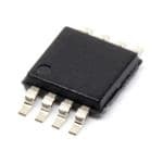
| 产品图片 |
|
| rohs | 符合RoHS无铅 / 符合限制有害物质指令(RoHS)规范要求 |
| 产品系列 | 放大器 IC,精密放大器,Analog Devices ADA4661-2ARMZ- |
| 数据手册 | |
| 产品型号 | ADA4661-2ARMZ |
| 产品种类 | 精密放大器 |
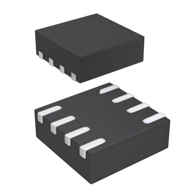
| 供应商器件封装 | 8-MSOP |
| 共模抑制比—最小值 | 140 dB |
| 包装 | 管件 |
| 压摆率 | 2 V/µs |
| 商标 | Analog Devices |
| 增益带宽生成 | 4 MHz |
| 增益带宽积 | 4MHz |
| 安装类型 | 表面贴装 |
| 安装风格 | SMD/SMT |
| 封装 | Tube |
| 封装/外壳 | 8-TSSOP,8-MSOP(0.118",3.00mm 宽) |
| 封装/箱体 | MSOP-8 |
| 工作温度 | -40°C ~ 125°C |
| 工作电源电压 | 18 V |
| 工厂包装数量 | 50 |
| 放大器类型 | 通用 |
| 最大双重电源电压 | 9 V |
| 最大工作温度 | + 125 C |
| 最小双重电源电压 | 1.5 V |
| 最小工作温度 | - 40 C |
| 标准包装 | 50 |
| 电压-电源,单/双 (±) | 3 V ~ 18 V, ±1.5 V ~ 9 V |
| 电压-输入失调 | 30µV |
| 电流-电源 | 630µA |
| 电流-输入偏置 | 0.5pA |
| 电流-输出/通道 | 220mA |
| 电源电压-最大 | 18 V |
| 电源电压-最小 | 3 V |
| 电源电流 | 630 uA |
| 电路数 | 2 |
| 转换速度 | 2 V/us |
| 输入偏压电流—最大 | 0.5 pA |
| 输入电压范围—最大 | 18 V |
| 输入补偿电压 | 30 uV |
| 输出电流 | 40 mA |
| 输出类型 | 满摆幅 |
| 通道数量 | 2 Channel |


- 商务部:美国ITC正式对集成电路等产品启动337调查
- 曝三星4nm工艺存在良率问题 高通将骁龙8 Gen1或转产台积电
- 太阳诱电将投资9.5亿元在常州建新厂生产MLCC 预计2023年完工
- 英特尔发布欧洲新工厂建设计划 深化IDM 2.0 战略
- 台积电先进制程称霸业界 有大客户加持明年业绩稳了
- 达到5530亿美元!SIA预计今年全球半导体销售额将创下新高
- 英特尔拟将自动驾驶子公司Mobileye上市 估值或超500亿美元
- 三星加码芯片和SET,合并消费电子和移动部门,撤换高东真等 CEO
- 三星电子宣布重大人事变动 还合并消费电子和移动部门
- 海关总署:前11个月进口集成电路产品价值2.52万亿元 增长14.8%


PDF Datasheet 数据手册内容提取
18 V, Precision, 725 µA, 4 MHz, CMOS RRIO Operational Amplifier Data Sheet ADA4661-2 FEATURES PIN CONNECTION DIAGRAMS Low power at high voltage (18 V): 725 μA maximum OUT A 1 8 V+ Low offset voltage –IN A 2 ADA4661-2 7 OUT B 135000 µµVV mmaaxxiimmuumm aotv VerS Ye/n2 tire common-mode range +INV A– 34 (NToOt Pto V SIEcWale) 65 –+IINN BB 11366-001 Low input bias current: 15 pA maximum Figure 1. 8-Lead MSOP Gain bandwidth product: 4 MHz typical at A = 100 V Unity-gain crossover: 4 MHz typical OUT A 1 8 V+ −3 dB closed-loop bandwidth: 2.1 MHz typical –IN A 2 ADA4661-2 7 OUT B Single-supply operation: 3 V to 18 V +IN A 3 TOP VIEW 6 –IN B (Not to Scale) Dual-supply operation: ±1.5 V to ±9 V V– 4 5 +IN B Unity-gain stable APPLICATIONS N1 . O CLTEOEANSVNEE ICTT U TNHCEO ENXNPEOCSTEEDD.PADTO V– OR 11366-002 Figure 2. 8-Lead LFCSP Current shunt monitors Active filters 250 VSY=18V Portable medical equipment 200 Buffer/level shifting 150 High impedance sensor interfaces 100 Battery powered instrumentation 50 V) (μS 0 O GENERAL DESCRIPTION V –50 The ADA4661-2 is a dual, precision, rail-to-rail input/output –100 amplifier optimized for low power, high bandwidth, and wide –150 operating supply voltage range applications. –200 The ADA4661-2 performance is guaranteed at 3.0 V, 10 V, –250 aapnpdl i1c8a tVio pnos wtheart s uuspep slyin vgolelt-aegnedse. dIt sius papnl ieexsc oefll 3en.3t Vse, l5e cVti, o1n0 fVo,r 1 2 0 1.5 3.0 4.5 6.0 7.5VC9M.0 (V1)0.5 12.0 13.5 15.0 16.5 18.0 11366-011 Figure 3. Input Offset Voltage vs. Common-Mode Voltage V and 15 V, and dual supplies of ±2.5 V, ±3.3 V, and ±5 V. It uses the Analog Devices, Inc., patented DigiTrim® trimming Table 1. Precision Low Power Op Amps (<1 mA) technique, which achieves low offset voltage. Additionally, the Supply Voltage 5 V 12 V to 16 V 30 V unique design architecture of the ADA4661-2 allows it to have Single ADA4505-1 OP196 OP777 excellent power supply rejection, common-mode rejection, and AD8500 offset voltage when operating in the common-mode voltage Dual ADA4505-2 AD8657 ADA4096-2 range of −V + 1.5 V to +V − 1.5 V. SY SY AD8502 OP296 OP727 The ADA4661-2 is specified over the extended industrial AD8506 ADA4661-2 AD8682 temperature range (−40°C to +125°C) and is available in ADA4666-2 AD8622 8-lead MSOP and 8-lead LFCSP (3 mm × 3 mm) packages. Quad ADA4505-4 AD8659 ADA4096-4 AD8504 OP496 OP747 AD8508 AD8684 AD8624 Rev. 0 Document Feedback Information furnished by Analog Devices is believed to be accurate and reliable. However, no responsibility is assumed by Analog Devices for its use, nor for any infringements of patents or other One Technology Way, P.O. Box 9106, Norwood, MA 02062-9106, U.S.A. rights of third parties that may result from its use. Specifications subject to change without notice. No license is granted by implication or otherwise under any patent or patent rights of Analog Devices. Tel: 781.329.4700 ©2013 Analog Devices, Inc. All rights reserved. Trademarks and registered trademarks are the property of their respective owners. Technical Support www.analog.com
ADA4661-2 Data Sheet TABLE OF CONTENTS Features .............................................................................................. 1 Input Stage ................................................................................... 22 Applications ....................................................................................... 1 Gain Stage .................................................................................... 23 General Description ......................................................................... 1 Output Stage ................................................................................ 23 Pin Connection Diagrams ............................................................... 1 Maximum Power Dissipation ................................................... 23 Revision History ............................................................................... 2 Rail-to-Rail Input and Output .................................................. 23 Specifications ..................................................................................... 3 Comparator Operation .............................................................. 24 Electrical Characteristics—18 V Operation ............................. 3 EMI Rejection Ratio .................................................................. 25 Electrical Characteristics—10 V Operation ............................. 5 Current Shunt monitor .............................................................. 25 Electrical Characteristics—3.0 V Operation ............................ 7 Active Filters ............................................................................... 25 Absolute Maximum Ratings ............................................................ 9 Capacitive Load Drive ............................................................... 26 Thermal Resistance ...................................................................... 9 Noise Considerations with High Impedance Sources ........... 28 ESD Caution .................................................................................. 9 Outline Dimensions ....................................................................... 29 Pin Configurations and Function Descriptions ......................... 10 Ordering Guide .......................................................................... 29 Typical Performance Characteristics ........................................... 11 Applications Information .............................................................. 22 REVISION HISTORY 7/13—Revision 0: Initial Version Rev. 0 | Page 2 of 32
Data Sheet ADA4661-2 SPECIFICATIONS ELECTRICAL CHARACTERISTICS—18 V OPERATION V = 18 V, V = V /2 V, T = 25°C, unless otherwise specified. SY CM SY A Table 2. Parameter Symbol Test Conditions/Comments Min Typ Max Unit INPUT CHARACTERISTICS Offset Voltage V 30 150 µV OS V = 1.5 V to 16.5 V 150 µV CM V = 1.5 V to 16.5 V; −40°C ≤ T ≤ +125°C 500 µV CM A V = 0 V to 18 V 300 µV CM V = 0 V to 18 V; −40°C ≤ T ≤ +125°C 600 µV CM A Offset Voltage Drift ΔV /ΔT −40°C ≤ T ≤ +125°C 0.6 3.1 μV/°C OS A Input Bias Current I 0.5 15 pA B −40°C ≤ T ≤ +85°C 100 pA A −40°C ≤ T ≤ +125°C 900 pA A Input Offset Current I 11 pA OS −40°C ≤ T ≤ +85°C 30 pA A −40°C ≤ T ≤ +125°C 300 pA A Input Voltage Range 0 18 V Common-Mode Rejection Ratio CMRR V = 1.5 V to 16.5 V 115 135 dB CM V = 1.5 V to 16.5 V; −40°C ≤ T ≤ +125°C 110 dB CM A V = 0 V to 18 V 100 118 dB CM V = 0 V to 18 V; −40°C ≤ T ≤ +125°C 91 dB CM A Large Signal Voltage Gain A R = 100 kΩ, V = 0.5 V to 17.5 V 120 147 dB VO L OUT −40°C ≤ T ≤ +125°C 120 dB A Input Resistance Differential Mode R >10 GΩ INDM Common Mode R >10 GΩ INCM Input Capacitance Differential Mode C 8.5 pF INDM Common Mode C 3 pF INCM OUTPUT CHARACTERISTICS Output Voltage High V R = 10 kΩ to V 17.95 17.97 V OH L CM −40°C ≤ T ≤ +125°C 17.94 V A R = 1 kΩ to V 17.6 17.79 V L CM −40°C ≤ T ≤ +125°C 17.58 V A Output Voltage Low V R = 10 kΩ to V 14 25 mV OL L CM −40°C ≤ T ≤ +125°C 40 mV A R = 1 kΩ to V 120 200 mV L CM −40°C ≤ T ≤ +125°C 300 mV A Continuous Output Current I Dropout voltage = 1 V 40 mA OUT Short-Circuit Current I Pulse width = 10 ms; refer to the Maximum ±220 mA SC Power Dissipation section Closed-Loop Output Impedance Z f = 100 kHz, A = 1 0.2 Ω OUT V POWER SUPPLY Power Supply Rejection Ratio PSRR V = 3.0 V to 18 V 120 145 dB SY −40°C ≤ T ≤ +125°C 120 dB A Supply Current per Amplifier I I = 0 mA 630 725 µA SY OUT −40°C ≤ T ≤ +125°C 975 µA A Rev. 0 | Page 3 of 32
ADA4661-2 Data Sheet Parameter Symbol Test Conditions/Comments Min Typ Max Unit DYNAMIC PERFORMANCE Slew Rate SR R = 1 kΩ, R = 10 kΩ, C = 10 pF, A = 1 2 V/µs S L L V Gain Bandwidth Product GBP V = 10 mV p-p, R = 10 kΩ, C = 10 pF, A = 100 4 MHz IN L L V Unity-Gain Crossover UGC V = 10 mV p-p, R = 10 kΩ, C = 10 pF, A = 1 4 MHz IN L L VO −3 dB Closed-Loop Bandwidth f V = 10 mV p-p, R = 10 kΩ, C = 10 pF, A = 1 2.1 MHz −3 dB IN L L V Phase Margin Φ V = 10 mV p-p, R = 10 kΩ, C = 10 pF, A = 1 60 Degrees M IN L L VO Settling Time to 0.1% t V = 1 V step, R = 10 kΩ, C = 10 pF 1.3 µs S IN L L Channel Separation CS V = 17.9 V p-p, f = 10 kHz, R = 10 kΩ 80 dB IN L EMI Rejection Ratio of +IN x EMIRR V = 100 mV peak (200 mV p-p) IN f = 400 MHz 34 dB f = 900 MHz 42 dB f = 1800 MHz 50 dB f = 2400 MHz 60 dB NOISE PERFORMANCE Total Harmonic Distortion Plus THD + N A = 1, V = 5.4 V rms at 1 kHz V IN Noise Bandwidth = 80 kHz 0.0004 % Bandwidth = 500 kHz 0.0008 % Peak-to-Peak Noise e p-p f = 0.1 Hz to 10 Hz 3 µV p-p n Voltage Noise Density e f = 1 kHz 18 nV/√Hz n f = 10 kHz 14 nV/√Hz Current Noise Density i f = 1 kHz 360 fA/√Hz n Rev. 0 | Page 4 of 32
Data Sheet ADA4661-2 ELECTRICAL CHARACTERISTICS—10 V OPERATION V = 10 V, V = V /2 V, T = 25°C, unless otherwise specified. SY CM SY A Table 3. Parameter Symbol Test Conditions/Comments Min Typ Max Unit INPUT CHARACTERISTICS Offset Voltage V 30 150 µV OS V = 1.5 V to 8.5 V 150 µV CM V = 1.5 V to 8.5 V; −40°C ≤ T ≤ +125°C 450 µV CM A V = 0 V to 10 V 300 µV CM V = 0 V to 10 V; −40°C ≤ T ≤ +125°C 600 µV CM A Offset Voltage Drift ΔV /ΔT −40°C ≤ T ≤ +125°C 0.6 3.1 μV/°C OS A Input Bias Current I 0.25 15 pA B −40°C ≤ T ≤ +85°C 80 pA A −40°C ≤ T ≤ +125°C 750 pA A Input Offset Current I 11 pA OS −40°C ≤ T ≤ +85°C 30 pA A −40°C ≤ T ≤ +125°C 270 pA A Input Voltage Range 0 10 V Common-Mode Rejection Ratio CMRR V = 1.5 V to 8.5 V 115 140 dB CM V = 1.5 V to 8.5 V; −40°C ≤ T ≤ +125°C 115 dB CM A V = 0 V to 10 V 95 114 dB CM V = 0 V to 10 V; −40°C ≤ T ≤ +125°C 86 dB CM A Large Signal Voltage Gain A R = 100 kΩ, V = 0.5 V to 9.5 V 120 145 dB VO L OUT −40°C ≤ T ≤ +125°C 120 dB A Input Resistance Differential Mode R >10 GΩ INDM Common Mode R >10 GΩ INCM Input Capacitance Differential Mode C 8.5 pF INDM Common Mode C 3 pF INCM OUTPUT CHARACTERISTICS Output Voltage High V R = 10 kΩ to V 9.96 9.98 V OH L CM −40°C ≤ T ≤ +125°C 9.96 V A R = 1 kΩ to V 9.7 9.88 V L CM −40°C ≤ T ≤ +125°C 9.7 V A Output Voltage Low V R = 10 kΩ to V 10 15 mV OL L CM −40°C ≤ T ≤ +125°C 30 mV A R = 1 kΩ to V 77 110 mV L CM −40°C ≤ T ≤ +125°C 200 mV A Continuous Output Current I Dropout voltage = 1 V 40 mA OUT Short-Circuit Current I Pulse width = 10 ms; refer to the Maximum ±220 mA SC Power Dissipation section Closed-Loop Output Impedance Z f = 100 kHz, A = 1 0.2 Ω OUT V POWER SUPPLY Power Supply Rejection Ratio PSRR V = 3.0 V to 18 V 120 145 dB SY −40°C ≤ T ≤ +125°C 120 dB A Supply Current per Amplifier I I = 0 mA 620 725 µA SY OUT −40°C ≤ T ≤ +125°C 975 µA A Rev. 0 | Page 5 of 32
ADA4661-2 Data Sheet Parameter Symbol Test Conditions/Comments Min Typ Max Unit DYNAMIC PERFORMANCE Slew Rate SR R = 1 kΩ, R = 10 kΩ, C = 10 pF, A = 1 1.8 V/µs S L L V Gain Bandwidth Product GBP V = 10 mV p-p, R = 10 kΩ, C = 10 pF, A = 100 4 MHz IN L L V Unity-Gain Crossover UGC V = 10 mV p-p, R = 10 kΩ, C = 10 pF, A = 1 4 MHz IN L L VO −3 dB Closed-Loop Bandwidth f V = 10 mV p-p, R = 10 kΩ, C = 10 pF, A = 1 2.1 MHz −3 dB IN L L V Phase Margin Φ V = 10 mV p-p, R = 10 kΩ, C = 10 pF, A = 1 60 Degrees M IN L L VO Settling Time to 0.1% t V = 1 V step, R = 10 kΩ, C = 10 pF 1.3 µs S IN L L Channel Separation CS V = 9.9 V p-p, f = 10 kHz, R = 10 kΩ 85 dB IN L EMI Rejection Ratio of +IN x EMIRR V = 100 mV peak (200 mV p-p) IN f = 400 MHz 34 dB f = 900 MHz 42 dB f = 1800 MHz 50 dB f = 2400 MHz 60 dB NOISE PERFORMANCE Total Harmonic Distortion Plus Noise THD + N A = 1, V = 2.2 V rms at 1 kHz V IN Bandwidth = 80 kHz 0.0004 % Bandwidth = 500 kHz 0.0008 % Peak-to-Peak Noise e p-p f = 0.1 Hz to 10 Hz 3 µV p-p n Voltage Noise Density e f = 1 kHz 18 nV/√Hz n f = 10 kHz 14 nV/√Hz Current Noise Density i f = 1 kHz 360 fA/√Hz n Rev. 0 | Page 6 of 32
Data Sheet ADA4661-2 ELECTRICAL CHARACTERISTICS—3.0 V OPERATION V = 3.0 V, V = V /2 V, T = 25°C, unless otherwise specified. SY CM SY A Table 4. Parameter Symbol Test Conditions/Comments Min Typ Max Unit INPUT CHARACTERISTICS Offset Voltage V 30 150 µV OS V = V /2; −40°C ≤ T ≤ +125°C 450 µV CM SY A V = 0 V to 3.0 V 300 µV CM V = 0 V to 3.0 V; −40°C ≤ T ≤ +125°C 600 µV CM A Offset Voltage Drift ΔV /ΔT −40°C ≤ T ≤ +125°C 0.6 3.1 μV/°C OS A Input Bias Current I 0.15 8 pA B −40°C ≤ T ≤ +85°C 45 pA A −40°C ≤ T ≤ +125°C 650 pA A Input Offset Current I 11 pA OS −40°C ≤ T ≤ +85°C 30 pA A −40°C ≤ T ≤ +125°C 270 pA A Input Voltage Range 0 3 V Common-Mode Rejection Ratio CMRR V = 0 V to 3.0 V 85 100 dB CM V = 0 V to 3.0 V; −40°C ≤ T ≤ +125°C 75 dB CM A Large Signal Voltage Gain A R = 100 kΩ, V = 0.5 V to 2.5 V 105 130 dB VO L OUT −40°C ≤ T ≤ +125°C 105 dB A Input Resistance Differential Mode R >10 GΩ INDM Common Mode R >10 GΩ INCM Input Capacitance Differential Mode C 8.5 pF INDM Common Mode C 3 pF INCM OUTPUT CHARACTERISTICS Output Voltage High V R = 10 kΩ to V 2.98 2.99 V OH L CM −40°C ≤ T ≤ +125°C 2.98 V A R = 1 kΩ to V 2.9 2.96 V L CM −40°C ≤ T ≤ +125°C 2.9 V A Output Voltage Low V R = 10 kΩ to V 4 8 mV OL L CM −40°C ≤ T ≤ +125°C 15 mV A R = 1 kΩ to V 25 40 mV L CM −40°C ≤ T ≤ +125°C 65 mV A Continuous Output Current I Dropout voltage = 1 V 30 mA OUT Short-Circuit Current I Pulse width = 10 ms; refer to the Maximum ±220 mA SC Power Dissipation section Closed-Loop Output Impedance Z f = 100 kHz, A = 1 0.2 Ω OUT V POWER SUPPLY Power Supply Rejection Ratio PSRR V = 3.0 V to 18 V 120 145 dB SY −40°C ≤ T ≤ +125°C 120 dB A Supply Current per Amplifier I I = 0 mA 615 725 µA SY OUT −40°C ≤ T ≤ +125°C 975 µA A DYNAMIC PERFORMANCE Slew Rate SR R = 1 kΩ, R = 10 kΩ, C = 10 pF, A = 1 1.7 V/µs S L L V Gain Bandwidth Product GBP V = 10 mV p-p, R = 10 kΩ, C = 10 pF, A = 100 4 MHz IN L L V Unity-Gain Crossover UGC V = 10 mV p-p, R = 10 kΩ, C = 10 pF, A = 1 4 MHz IN L L VO −3 dB Closed-Loop Bandwidth f V = 10 mV p-p, R = 10 kΩ, C = 10 pF, A = 1 1.7 MHz −3 dB IN L L V Phase Margin Φ V = 10 mV p-p, R = 10 kΩ, C = 10 pF, A = 1 60 Degrees M IN L L VO Settling Time to 0.1% t V = 1 V step, R = 10 kΩ, C = 10 pF 1.3 µs S IN L L Channel Separation CS V = 2.9 V p-p, f = 10 kHz, R = 10 kΩ 90 dB IN L Rev. 0 | Page 7 of 32
ADA4661-2 Data Sheet Parameter Symbol Test Conditions/Comments Min Typ Max Unit EMI Rejection Ratio of +IN x EMIRR V = 100 mV peak (200 mV p-p) IN f = 400 MHz 34 dB f = 900 MHz 42 dB f = 1800 MHz 50 dB f = 2400 MHz 60 dB NOISE PERFORMANCE Total Harmonic Distortion Plus Noise THD + N A = 1, V = 0.44 V rms at 1 kHz V IN Bandwidth = 80 kHz 0.002 % Bandwidth = 500 kHz 0.003 % Peak-to-Peak Noise e p-p f = 0.1 Hz to 10 Hz 3 µV p-p n Voltage Noise Density e f = 1 kHz 18 nV/√Hz n f = 10 kHz 14 nV/√Hz Current Noise Density i f = 1 kHz 360 fA/√Hz n Rev. 0 | Page 8 of 32
Data Sheet ADA4661-2 ABSOLUTE MAXIMUM RATINGS THERMAL RESISTANCE Table 5. θ is specified for the worst-case conditions, that is, a device Parameter Rating JA soldered in a circuit board for surface-mount packages using a Supply Voltage 20.5 V standard 4-layer JEDEC board. The exposed pad of the LFCSP Input Voltage (V−) − 300 mV to (V+) + 300 mV package is soldered to the board. Input Current1 ±10 mA Differential Input Voltage Limited by maximum input Table 6. Thermal Resistance current Package Type θ θ Unit JA JC Output Short-Circuit Refer to the Maximum Power 8-Lead MSOP 142 45 °C/W Duration to GND Dissipation section 8-Lead LFCSP 83.5 48.51 °C/W Temperature Range Storage −65°C to +150°C 1 θJC is measured on the top surface of the package. Operating −40°C to +125°C Junction −65°C to +150°C ESD CAUTION Lead Temperature 300°C (Soldering, 60 sec) ESD Human Body Model2 4 kV Machine Model3 400 V Field-Induced Charged- 1.25 kV Device Model (FICDM)4 1 The input pins have clamp diodes to the power supply pins and to each other. Limit the input current to 10 mA or less when input signals exceed the power supply rail by 0.3 V. 2 Applicable standard: MIL-STD-883, Method 3015.7. 3 Applicable standard: JESD22-A115-A (ESD machine model standard of JEDEC). 4 Applicable Standard JESD22-C101C (ESD FICDM standard of JEDEC). Stresses above those listed under Absolute Maximum Ratings may cause permanent damage to the device. This is a stress rating only; functional operation of the device at these or any other conditions above those indicated in the operational section of this specification is not implied. Exposure to absolute maximum rating conditions for extended periods may affect device reliability. Rev. 0 | Page 9 of 32
ADA4661-2 Data Sheet PIN CONFIGURATIONS AND FUNCTION DESCRIPTIONS OUT A 1 8 V+ –IN A 2 7 OUT B ADA4661-2 +IN A 3 TOP VIEW 6 –IN B OUT A 1 8 V+ V– 4 (Not to Scale) 5 +IN B –IN A 2 ADA4661-2 7 OUT B +INV A– 34 (NToOt Pto V SIEcWale) 65 –+IINN BB 11366-004 N1 . O CLTEOEANSVNEE ICTT U TNHCEO ENXNPEOCSTEEDD.PADTO V– OR 11366-005 Figure 4. Pin Configuration, 8-Lead MSOP Figure 5. Pin Configuration, 8-Lead LFCSP Table 7. Pin Function Descriptions Pin No.1 8-Lead MSOP 8-Lead LFCSP Mnemonic Description 1 1 OUT A Output, Channel A. 2 2 −IN A Negative Input, Channel A. 3 3 +IN A Positive Input, Channel A. 4 4 V− Negative Supply Voltage. 5 5 +IN B Positive Input, Channel B. 6 6 −IN B Negative Input, Channel B. 7 7 OUT B Output, Channel B. 8 8 V+ Positive Supply Voltage. N/A 92 EPAD Exposed Pad. For the 8-lead LFCSP only, connect the exposed pad to V− or leave it unconnected. 1 N/A means not applicable. 2 The exposed pad is not shown in the pin configuration diagram, Figure 5. Rev. 0 | Page 10 of 32
Data Sheet ADA4661-2 TYPICAL PERFORMANCE CHARACTERISTICS T = 25°C, unless otherwise noted. A 80 90 VSY=3V VSY = 18V 70 VCM= VSY/2 80 VCM = VSY/2 600 CHANNELS 600 CHANNELS 70 S 60 S R R E E FI FI 60 LI 50 LI P P M M 50 A A F 40 F R O R O 40 BE 30 BE M M 30 U U N 20 N 20 10 10 0 0 0 0 0 0 0 0 0 0 0 0 0 0 0 0 0 0 0 0 0 0 0 0 0 0 0 0 0 0 0 0 –14 –12 –10 –8 –6 –4 –2VOS (µV)2 4 6 8 10 12 1411366-006 –14 –12 –10 –8 –6 –4 –2VOS (µV)2 4 6 8 10 12 1411366-009 Figure 6. Input Offset Voltage Distribution Figure 9. Input Offset Voltage Distribution 18 18 VSY = 3V VSY = 18V 16 VCM = VSY/2 16 VCM = VSY/2 –40°C ≤ TA ≤ +125°C –40°C ≤ TA ≤ +125°C S 14 100 CHANNELS S 14 100 CHANNELS R R E E FI 12 FI 12 LI LI P P M 10 M 10 A A F F R O 8 R O 8 E E B B M 6 M 6 U U N N 4 4 2 2 0 0 0 0.2 0.4 0.6 0.8 T1C.0VO1S. 2(µV/1°.C4) 1.6 1.8 2.0 2.2 2.4 11366-007 0 0.2 0.4 0.6 0.8 T1C.0VO1S. 2(µV/1°.C4) 1.6 1.8 2.0 2.2 2.4 11366-010 Figure 7. Input Offset Voltage Drift Distribution Figure 10. Input Offset Voltage Drift Distribution 250 250 VSY = 3V VSY=18V 200 20 CHANNELS 200 20 CHANNELS 150 150 100 100 50 50 V) V) μ μ (S 0 (S 0 O O V V –50 –50 –100 –100 –150 –150 –200 –200 –2500 0.3 0.6 0.9 1.2 VC1M.5 (V)1.8 2.1 2.4 2.7 3.0 11366-008 –2500 1.5 3.0 4.5 6.0 7.5VC9M.0 (V1)0.5 12.0 13.5 15.0 16.5 18.0 11366-011 Figure 8. Input Offset Voltage vs. Common-Mode Voltage Figure 11. Input Offset Voltage vs. Common-Mode Voltage Rev. 0 | Page 11 of 32
ADA4661-2 Data Sheet 350 350 VSY=18V VSY=3V 20 CHANNELSAT –40°CAND +85°C 20 CHANNELSAT –40°CAND +85°C 250 250 150 150 V) 50 (μV)OS 50 V (μOS –50 V –50 –150 –150 –250 –250 –350 –3500 0.3 0.6 0.9 1.2 VC1M.5 (V)1.8 2.1 2.4 2.7 3.0 11366-012 0 1.5 3.0 4.5 6.0 7.5VCM9.0 (V)10.5 12.0 13.5 15.0 16.5 18.011366-015 Figure 12. Input Offset Voltage vs. Common-Mode Voltage Figure 15. Input Offset Voltage vs. Common-Mode Voltage 350 350 VSY=18V VSY=3V 20 CHANNELSAT –40°CAND +125°C 20 CHANNELSAT –40°CAND +125°C 250 250 150 150 V) 50 (μV)OS 50 (μVOS –50 V –50 –150 –150 –250 –250 –350 –3500 0.3 0.6 0.9 1.2 VC1M.5 (V)1.8 2.1 2.4 2.7 3.0 11366-013 0 1.5 3.0 4.5 6.0 7.5VCM9.0 (V)10.5 12.0 13.5 15.0 16.5 18.011366-016 Figure 13. Input Offset Voltage vs. Common-Mode Voltage Figure 16. Input Offset Voltage vs. Common-Mode Voltage 0 0 VSY = 10V –20 VSY=10V –20 ΔVCM = 400mV ΔVSY = 400mV B) B) –40 R (d –40 R (d –60 PSRR– R R PSRR+ M S AL C –60 AL P –80 N N SIG –80 SIG–100 ALL ALL–120 M–100 M S S –140 –120 –160 –1400 1 2 3 4 VCM5 (V) 6 7 8 9 10 11366-216 –1800 1 2 3 4 VCM5 (V) 6 7 8 9 10 11366-168 Figure 14. Small Signal CMRR vs. Common-Mode Voltage Figure 17. Small Signal PSRR vs. Common-Mode Voltage Rev. 0 | Page 12 of 32
Data Sheet ADA4661-2 1000 1000 VSY = 3V VSY = 18V VCM = VSY/2 VCM = VSY/2 100 100 A) A) (pB10 (pB10 I I |IB–| |IB–| |IB+| |IB+| 1 1 0.125 50 TEMPERA75TURE (°C) 100 125 11366-014 0.125 50 TEMPERA75TURE (°C) 100 125 11366-017 Figure 18. Input Bias Current vs. Temperature Figure 21. Input Bias Current vs. Temperature 3 3 VSY = 3V VSY = 18V 2 VCM = VSY/2 2 VCM = VSY/2 1 1 A) 0 A) 0 n n (B (B I –1 I –1 25°C –2 85°C –2 25°C 125°C 85°C 125°C –3 –3 –40 0.5 1.0 VC1M.5 (V) 2.0 2.5 3.0 11366-018 –40 2 4 6 8VCM (V1)0 12 14 16 18 11366-021 Figure 19. Input Bias Current vs. Common-Mode Voltage Figure 22. Input Bias Current vs. Common-Mode Voltage 10000 10000 V) V) L (m VSY=3V L (m VSY= 18V AI AI R R LY 1000 LY 1000 P P P P U U S S O O T T )H 100 )H 100 O O V V E ( –40°C E ( –40°C G +25°C G +25°C TA +85°C TA +85°C L +125°C L +125°C O 10 O 10 V V T T U U P P T T U U O O 01.001 0.01 LOA0.D1 CURRENT1 (mA) 10 100 11366-019 01.001 0.01 LOA0.D1 CURRENT1 (mA) 10 100 11366-022 Figure 20. Output Voltage (VOH) to Supply Rail vs. Load Current Figure 23. Output Voltage (VOH) to Supply Rail vs. Load Current Rev. 0 | Page 13 of 32
ADA4661-2 Data Sheet 10000 10000 V) V) L (m VSY=3V L (m VSY= 18V AI AI R 1000 R 1000 Y Y L L P P –40°C UP –40°C UP +25°C O S 100 ++2855°°CC O S 100 ++8152°5C°C T +125°C T )L )L O O V V E ( 10 E ( 10 G G A A T T L L O O V V T 1 T 1 U U P P T T U U O O 0.01.001 0.01 LOA0.D1 CURRENT1 (mA) 10 100 11366-020 0.01.001 0.01 LOA0.D1 CURRENT1 (mA) 10 100 11366-023 Figure 24. Output Voltage (VOL) to Supply Rail vs. Load Current Figure 27. Output Voltage (VOL) to Supply Rail vs. Load Current 3.00 18.00 2.99 RL=10kΩ 17.95 RL=10kΩ V) V) ) (H ) (H O2.98 O17.90 V V E ( E ( G G A A LT2.97 LT17.85 O O V V T T TPU2.96 RL=1kΩ TPU17.80 RL=1kΩ U U O O 2.95 17.75 VSY=3V VSY=18V 2.94–50 –25 0 TEM2P5ERATUR5E0 (°C) 75 100 125 11366-024 17.70–50 –25 0 TEM2P5ERATUR5E0 (°C) 75 100 125 11366-027 Figure 25. Output Voltage (VOH) vs. Temperature Figure 28. Output Voltage (VOH) vs. Temperature 50 200 VSY=3V 180 VSY=18V V) 40 V)160 m m ) (OL RL=1kΩ ) (OL140 RL=1kΩ V V E ( 30 E (120 G G LTA LTA100 O O V 20 V 80 T T U U TP TP 60 U U O 10 O 40 RL=10kΩ RL=10kΩ 20 0–50 –25 0 TEM2P5ERATUR5E0 (°C) 75 100 125 11366-025 0–50 –25 0 TEM2P5ERATUR5E0 (°C) 75 100 125 11366-028 Figure 26. Output Voltage (VOL) vs. Temperature Figure 29. Output Voltage (VOL) vs. Temperature Rev. 0 | Page 14 of 32
Data Sheet ADA4661-2 1000 1000 VSY=3V VSY= 18V 900 900 800 800 A) A) μ 700 μ 700 R ( R ( FIE 600 FIE 600 LI LI P 500 P 500 M M A A R 400 R 400 E E P P I SY 300 –+4205°°CC I SY 300 –+4205°°CC +85°C +85°C 200 +125°C 200 +125°C 100 100 0 0 0 0.5 1.0 VC1M.5 (V) 2.0 2.5 3.0 11366-026 0 3 6 VCM9 (V) 12 15 18 11366-029 Figure 30. Supply Current vs. Common-Mode Voltage Figure 33. Supply Current vs. Common-Mode Voltage 1000 1000 VCM = VSY/2 900 VCM = VSY/2 800 800 µA) µA) 700 R ( R ( FIE 600 FIE 600 LI LI P P 500 M M A A R 400 R 400 PE PE VSY= 3V I SY –+4205°°CC I SY 300 VVSSYY== 1108VV 200 +85°C 200 +125°C 100 0 0 0 2 4 6 8VSY (V1)0 12 14 16 18 11366-030 –50 –25 0 TEM2P5ERATUR5E0 (°C) 75 100 125 11366-133 Figure 31. Supply Current vs. Supply Voltage Figure 34. Supply Current vs. Temperature 80 135 80 135 VRSLY = = 1 03kVΩ RVSLY = = 1 01k8ΩV PHASE PHASE 60 90 60 90 B) B) P GAIN (d 40 45 Degrees) P GAIN (d 40 45 Degrees) PEN-LOO 20 GAIN 0 PHASE ( PEN-LOO 20 GAIN 0 PHASE ( O O 0 –45 0 –45 CL = 0pF CL =0pF CL = 10pF CL =10pF CL = 0pF CL =0pF –2010k CL = 10pF 100kFREQUENCY (Hz)1M 10M–90 11366-033 –2010k CL =10pF 100kFREQUENCY (Hz)1M 10M–90 11366-036 Figure 32. Open-Loop Gain and Phase vs. Frequency Figure 35. Open-Loop Gain and Phase vs. Frequency Rev. 0 | Page 15 of 32
ADA4661-2 Data Sheet 60 60 VSY = 3V VSY = 18V CL = 5pF CL = 5pF AV=100 AV=100 40 40 AV=10 AV=10 B) 20 B) 20 d d N ( N ( GAI AV=1 GAI AV=1 0 0 –20 –20 –401k 10k FREQU1E00NkCY (Hz) 1M 10M 11366-232 –401k 10k FREQU1E00NkCY (Hz) 1M 10M 11366-235 Figure 36. Closed-Loop Gain vs. Frequency Figure 39. Closed-Loop Gain vs. Frequency 10k 10k VSY = 3V VSY = 18V VCM = VSY/2 VCM = VSY/2 1k 1k 100 100 Ω) Ω) (UT10 AV = 100 (UT10 AV = 100 O O Z Z 1 AV = 10 1 AV = 1 AV = 10 AV = 1 0.1 0.1 0.01100 1k F1R0EkQUENCY1 (0H0zk) 1M 10M 11366-038 0.01100 1k F1R0EkQUENCY1 (0H0zk) 1M 10M 11366-041 Figure 37. Output Impedance vs. Frequency Figure 40. Output Impedance vs. Frequency 120 120 100 100 80 80 B) B) d d R ( 60 R ( 60 R R M M C C 40 40 20 20 VSY = 3V VSY = 18V VCM = VSY/2 VCM = VSY/2 0100 1k F1R0EkQUENCY1 (0H0zk) 1M 10M 11366-039 0100 1k F1R0EkQUENCY1 (0H0zk) 1M 10M 11366-042 Figure 38. CMRR vs. Frequency Figure 41. CMRR vs. Frequency Rev. 0 | Page 16 of 32
Data Sheet ADA4661-2 100 100 VSY = 3V PSRR+ VSY = 18V PSRR+ PSRR– PSRR– 80 80 B) 60 B) 60 d d R ( R ( R R S S P 40 P 40 20 20 01k 10k FREQU1E00NkCY (Hz) 1M 10M 11366-040 01k 10k FREQU1E00NkCY (Hz) 1M 10M 11366-043 Figure 42. PSRR vs. Frequency Figure 45. PSRR vs. Frequency 60 60 VSY = 3V VSY = 18V VIN = 100mV p-p VIN = 100mV p-p AV = 1 AV = 1 50 RL = 10kΩ 50 RL = 10kΩ OS– %) 40 %) 40 T ( T ( O O OS– O O H 30 OS+ H 30 S S R R E E OV 20 OV 20 OS+ 10 10 00 10 CA2P0ACITANCE3 (0pF) 40 50 11366-044 00 10 CA2P0ACITANCE3 (0pF) 40 50 11366-047 Figure 43. Small Signal Overshoot vs. Load Capacitance Figure 46. Small Signal Overshoot vs. Load Capacitance VSY = ±1.5V VSY = ±9V VIN = 2.5V p-p VIN = 17V p-p AV = 1 AV = 1 RL = 10kΩ RL = 10kΩ CL = 10pF CL = 10pF RS = 1kΩ RS = 1kΩ VOLTAGE (0.5V/DIV) VOLTAGE (2V/DIV) TIME (5µs/DIV) 11366-045 TIME (5µs/DIV) 11366-048 Figure 44. Large Signal Transient Response Figure 47. Large Signal Transient Response Rev. 0 | Page 17 of 32
ADA4661-2 Data Sheet V) V) DI DI V/ V/ m m 0 0 2 2 E ( E ( G G A A T T L L O O V V VSY = ±1.5V VSY = ±9V VIN = 100mV p-p VIN = 100mV p-p AV = 1 AV = 1 RL = 10kΩ RL = 10kΩ CTLI M= E1 0(2pµFs/DIV) 11366-046 CTLIM =E 1 (02pµFs/DIV) 11366-049 Figure 48. Small Signal Transient Response Figure 51. Small Signal Transient Response 0.2 3.5 1 18 0 3.0 0 15 VIN –0.2 2.5 OLTAGE (V)––00..64 VOUT 12..50 VOLTAGE (V) OLTAGE (V) ––21 VVOINUT 912 VOLTAGE (V) T V UT T V –3 6 UT PU–0.8 1.0 TP PU TP N U N U I O I –4 3 O –1 0.5 VSY = ±1.5V VSY = ±9V –1.2 ARVL == 1–01k0Ω 0 –5 ARVL == 1–01k0Ω 0 CL = 10pF CL = 10pF –1.4 VIN = 225mV TIME (2µs/DIV) –0.5 11366-050 –6 VIN = 1.35V TIME (2µs/DIV) –3 11366-053 Figure 49. Positive Overload Recovery Figure 52. Positive Overload Recovery 0.4 2.0 2 9 VIN VIN 0.2 1.5 1 6 0 1.0 NPUT VOLTAGE (V)–––000...642 –000.5.5 UTPUT VOLTAGE (V) NPUT VOLTAGE (V) ––210 03–3 UTPUT VOLTAGE (V) I O I –3 –6 O –0.8 –1.0 ––11..20 VOUT TIME (2µs/DIV) AVRCVSIVLLNY === == 11– 200±12kp105Ω.Fm5VV ––21..05 11366-051 ––54 VOUT TIME (2µs/DIV) ARCVVSIVLLNY === == 11– 100±1.kp930ΩV5FV ––192 11366-054 Figure 50. Negative Overload Recovery Figure 53. Negative Overload Recovery Rev. 0 | Page 18 of 32
Data Sheet ADA4661-2 INPUT INPUT mV/DIV) V/DIV) mV/DIV) V/DIV) 0 m 0 m 0 1 0 1 E (5 OUTPUT GE ( E (5 OUTPUT GE ( G A G A A T A T T L T L L O L O O V O V V V ERROR BAND VSY = ±1.5V ERROR BAND VSY = ±9V VIN = 1V p-p VIN = 1V p-p RL = 10kΩ RL = 10kΩ TIME (400ns/DIV) CALV == 1–01pF 11366-052 TIME (400ns/DIV) CALV == 1–01pF 11366-055 Figure 54. Positive Settling Time to 0.1% Figure 57. Positive Settling Time to 0.1% INPUT INPUT E (500mV/DIV) OUTPUT GE (1mV/DIV) E (500mV/DIV) OUTPUT GE (1mV/DIV) G ERROR BAND A G ERROR BAND A LTA OLT LTA OLT O V O V V V VSY = ±1.5V VSY = ±9V VIN = 1V p-p VIN = 1V p-p RL = 10kΩ RL = 10kΩ TIME (400ns/DIV) CALV == 1–01pF 11366-056 TIME (400ns/DIV) CALV == 1–01pF 11366-059 Figure 55. Negative Settling Time to 0.1% Figure 58. Negative Settling Time to 0.1% 1k 1k VSY = 3V VSY = 18V VCM = VSY/2 VCM = VSY/2 Hz) AV = 1 Hz) AV = 1 V/√ V/√ n n Y (100 Y (100 T T SI SI N N E E D D E E S S OI OI N N E 10 E 10 G G A A LT LT O O V V 110 100 1kFREQU1E0NkCY (Hz1)00k 1M 10M 11366-057 110 100 1kFREQU1E0NkCY (Hz1)00k 1M 10M 11366-060 Figure 56. Voltage Noise Density vs. Frequency Figure 59. Voltage Noise Density vs. Frequency Rev. 0 | Page 19 of 32
ADA4661-2 Data Sheet VSY = 3V VSY = 18V VCM = VSY/2 VCM = VSY/2 AV = 1 AV = 1 V) V) DI DI V/ V/ E (1µ E (1µ G G A A OLT OLT V V TIME (2s/DIV) 11366-058 TIME (2s/DIV) 11366-061 Figure 60. 0.1 Hz to 10 Hz Noise Figure 63. 0.1 Hz to 10 Hz Noise 3.5 20 18 3.0 16 V)2.5 V) 14 WING (2.0 WING ( 12 S S 10 T T TPU1.5 TPU 8 U U O O 1.0 6 VSY = 3V 4 VSY = 18V 0.5 VRCILLN === 11200.kp9ΩVF 2 VRCILLN === 111007kp.Ω9FV AV = 1 AV = 1 010 100 F1RkEQUENCY 1(0Hkz) 100k 1M 11366-062 010 100 F1RkEQUENCY 1(0Hkz) 100k 1M 11366-065 Figure 61. Output Swing vs. Frequency Figure 64. Output Swing vs. Frequency 1 1 VASVY = = 1 3V 8500k0HkHz zL LOOWW-P-PAASSSS F FILITLTEERR AVSVY = = 1 18V 8500k0HkHz zL LOOWW-P-PAASSSS F FILITLTEERR RL = 10kΩ RL = 10kΩ VIN = 440mV rms VIN = 5.4V rms 0.1 0.1 %) %) N ( N ( + + 0.01 D D H H T T 0.01 0.001 0.00110 100 FREQUE1kNCY (Hz) 10k 100k 11366-063 0.000110 100 FREQUE1kNCY (Hz) 10k 100k 11366-066 Figure 62. THD + N vs. Frequency Figure 65. THD + N vs. Frequency Rev. 0 | Page 20 of 32
Data Sheet ADA4661-2 100 100 VSY = 3V VSY = 18V AV = 1 AV = 1 RL = 10kΩ RL = 10kΩ f = 1kHz 10 f = 1kHz 10 1 %) 1 %) N ( N ( + + 0.1 D D H H T0.1 T 0.01 0.01 0.001 80kHz LOW-PASS FILTER 80kHz LOW-PASS FILTER 500kHz LOW-PASS FILTER 500kHz LOW-PASS FILTER 0.0001.001 0.01 AMPLITU0D.1E (V rms) 1 10 11366-064 0.00001.001 0.01 AMPLITU0D.1E (V rms) 1 10 11366-067 Figure 66. THD + N vs. Amplitude Figure 68. THD + N vs. Amplitude 0 0 VIN = 0.5V p-p VIN = 0.5V p-p VIN = 1.5V p-p VIN = 9V p-p –20 VIN = 2.9V p-p –20 VIN = 17.9V p-p dB) –40 dB) –40 N ( N ( O O TI –60 TI –60 A A R R A A P –80 P –80 E E S S L L E–100 E–100 N N N N A A CH–120 CH–120 VSY = 3V VSY = 18V –140 AV = 100 –140 AV = 100 RL = 10kΩ RL = 10kΩ 500kHz LOW-PASS FILTER 500kHz LOW-PASS FILTER –16010 100 FREQUE1kNCY (Hz) 10k 100k 11366-068 –16010 100 FREQUE1kNCY (Hz) 10k 100k 11366-069 Figure 67. Channel Separation vs. Frequency Figure 69. Channel Separation vs. Frequency Rev. 0 | Page 21 of 32
ADA4661-2 Data Sheet APPLICATIONS INFORMATION V+ HIGH VOLTAGE PROTECTION M19 M20 I2 M11 M12 M17 M18 M22 +IN x R1 M9 M10 C1 C2 M3 M4 Q1 Q2 D1 D2 OUT x V1 C3 –IN x R2 M1 M2 M7 M8 M21 M15 M16 I1 M5 M6 I3 HIGH VOLTAGE PROTECTION V– M13 M14 11366-169 Figure 70. Simplified Schematic The ADA4661-2 is a low power, rail-to-rail input and output, graphs (see Figure 8, Figure 11, Figure 12, Figure 13, Figure 15, precision CMOS amplifier that operates over a wide supply and Figure 16). The CMRR performance benefits of the reduced voltage range of 3 V to 18 V. This amplifier uses the Analog common-mode range are guaranteed at final test and shown in the Devices DigiTrim technique to achieve a higher degree of electrical characteristics (see Table 2 to Table 4). precision than is available from other CMOS amplifiers. The For most of the input common-mode voltage range, the PMOS DigiTrim technique is a method of trimming the offset voltage differential pair is active. When the input common-mode of an amplifier after assembly. The advantage of postpackage voltage is within a few volts of the power supplies, the input trimming is that it corrects any offset voltages caused by transistors are exposed to these voltage changes. As the mechanical stresses of assembly. To achieve a rail-to-rail input common-mode voltage approaches the positive power supply, and output range with very low supply current, the ADA4661-2 the active differential pair changes from the PMOS pair to the uses unique input and output stages. NMOS pair. Differential pairs commonly exhibit different offset INPUT STAGE voltages. The handoff of control from one differential pair to the other creates a step like characteristic that is visible in the V vs. Figure 70 shows the simplified schematic of the ADA4661-2. OS V graphs (see Figure 8, Figure 11, Figure 12, Figure 13, Figure 15, The amplifier uses a three-stage architecture with a fully CM and Figure 16). This characteristic is inherent in all rail-to-rail differential input stage to achieve excellent dc performance input amplifiers that use the dual differential pair topology. specifications. Additional steps in the V vs. V graphs are visible as the The input stage comprises two differential transistor pairs— OS CM common-mode voltage approaches the negative power supply. a NMOS pair (M1, M2) and a PMOS pair (M3, M4)—and These changes are a result of the load transistors (M5, M6) folded-cascode transistors (M5 to M12). The input common- running out of headroom. As the load transistors are forced into mode voltage determines which differential pair is active. The the triode region of operation, the mismatch of their drain PMOS differential pair is active for most of the input common- impedance becomes a significant portion of the amplifier offset. mode range. The NMOS pair is required for input voltages up This effect can also be seen in the V vs. V graphs (see Figure 8, to and including the upper supply rail. This topology allows the OS CM Figure 11, Figure 12, Figure 13, Figure 15, and Figure 16). amplifier to maintain a wide dynamic input voltage range and maximize signal swing to both supply rails. Current Source I2 drives the PMOS transistor pair. As the input common-mode voltage approaches the upper power supply, The proprietary high voltage protection circuitry in the this current is reduced to zero. At the same time, a replica ADA4661-2 minimizes the common-mode voltage changes current source, I1, is increased from zero to enable the NMOS seen by the amplifier input stage for most of the input common- transistor pair. mode range. This results in the amplifier having excellent disturbance rejection when operating in this preferred The ADA4661-2 achieves its high performance specifications by common-mode range. The performance benefits of operating using low voltage MOS devices for its differential inputs. These within this preferred range are shown in the PSRR vs. V (see low voltage MOS devices offer excellent noise and bandwidth CM Figure 17), CMRR vs. V (see Figure 14), and V vs. V per unit of current. The input stage is isolated from the high CM OS CM Rev. 0 | Page 22 of 32
Data Sheet ADA4661-2 system voltages with proprietary protection circuitry. This regu- destroy the device. To ensure proper operation, it is necessary to lation circuitry protects the input devices from the high supply observe the maximum power derating curves. Figure 71 shows voltages at which the amplifier can operate. the maximum safe power dissipation in the package vs. the ambient temperature on a standard 4-layer JEDEC board. The The input devices are also protected from large differential exposed pad of the LFCSP package is soldered to the board. input voltages by clamp diodes (D1 and D2). These diodes are buffered from the inputs with two 120 Ω resistors (R1 and R2). 1.6 The diodes conduct significant current whenever the differen- TJMAX=150°C 1.4 tial voltage exceeds approximately 600 mV; in this condition, W) the differential input resistance falls to 240 Ω. It is possible for a ON ( 1.2 8-LEADLFCSP TI θJA=83.5°C/W significant amount of current to flow through these protection SIPA 1.0 diodes. The user must ensure that current flowing into the input DIS pins is limited to the absolute maximum of 10 mA. ER 0.8 W GAIN STAGE M PO 0.6 8θJ-LAE=A1D42M°SCO/WP U The second stage of the amplifier is composed of an NPN M 0.4 XI differential pair (Q1, Q2) and folded-cascode transistors (M13 MA 0.2 to M20). The amplifier features nested Miller compensation (OCU1 TtoP CU3T). STAGE 00 25 AMB50IENT TEM7P5ERATUR1E0 0(°C) 125 150 11366-371 Figure 71. Maximum Power Dissipation vs. Ambient Temperature The ADA4661-2 features a complementary output stage consisting of the M21 and M22 transistors. These transistors are configured Refer to Technical Article MS-2251, Data Sheet Intricacies— in a Class AB topology and are biased by the voltage source, V1. Absolute Maximum Ratings and Thermal Resistances, for more This topology allows the output voltage to go within millivolts information. of the supply rails, achieving a rail-to-rail output swing. The RAIL-TO-RAIL INPUT AND OUTPUT output voltage is limited by the output impedance of the transis- The ADA4661-2 features rail-to-rail input and output with a tors, which are low R MOS devices. The output voltage swing ON supply voltage from 3 V to 18 V. Figure 72 shows the input and is a function of the load current and can be estimated using the output waveforms of the ADA4661-2 configured as a unity-gain output voltage to supply rail vs. load current graphs (see Figure 20, buffer with a supply voltage of ±9 V. With an input voltage of Figure 23, Figure 24, and Figure 27). The high voltage and high ±9 V, the ADA4661-2 allows the output to swing very close to current capability of the ADA4661-2 output stage requires the both rails. Additionally, it does not exhibit phase reversal. user to ensure that it operates within the thermal safe operating area (see the Maximum Power Dissipation section). 10 VIN 8 VOUT MAXIMUM POWER DISSIPATION 6 The ADA4661-2 is capable of driving an output current up 4 to 220 mA. However, the usable output load current drive is limited to the maximum power dissipation allowed by the E (V) 2 device package. The absolute maximum junction temperature AG 0 T for the ADA4661-2 is 150°C (see Table 5). The junction VOL –2 temperature can be estimated as follows: –4 TJ = PD × θJA + TA –6 VSY = ±9V VIN = ±9V The power dissipated in the package (PD) is the sum of the –8 RAVL == 110kΩ qouutiepsucte sntta gpeo wtrearn dsiisstsoipr.a Itti ocnan a nbed cthalec uploawteedr adsi sfsoilploatwesd: by the –10 CL = 10pF TIME (200µs/DIV) 11366-072 Figure 72. Rail-to-Rail Input and Output P = (V × I ) + (V − V ) × I D SY SY SY OUT LOAD where: V is the power supply rail. SY ISY is the quiescent current. V is the output of the amplifier. OUT I is the output load. LOAD Do not exceed the maximum junction temperature for the device, 150°C. Exceeding the junction temperature limit can cause degradation in the parametric performance or even Rev. 0 | Page 23 of 32
ADA4661-2 Data Sheet COMPARATOR OPERATION Figure 75 and Figure 76 show the ADA4661-2 configured as a comparator, with 100 kΩ resistors in series with the input pins. An op amp is designed to operate in a closed-loop configuration Any unused channels are configured as buffers with the input with feedback from its output to its inverting input. Figure 73 voltage kept at the midpoint of the power supplies. shows the ADA4661-2 configured as a voltage follower with an input voltage that is always kept at the midpoint of the power +VSY supplies. The same configuration is applied to the unused channel. A1 and A2 indicate the placement of ammeters to measure supply current. I + refers to the current flowing from 100kΩ A1 ISY+ SY the upper supply rail to the op amp, and I − refers to the SY current flowing from the op amp to the lower supply rail. As ADA4661-2 VOUT shown in Figure 74, in normal operating conditions, the total 1/2 current flowing into the op amp is equivalent to the total current flowing out of the op amp, where I + = I − = 630 μA per amplifier 100kΩ A2 ISY– SY SY at V = 18 V. SY +VSY –VSY 11366-268 Figure 75. Comparator A A1 ISY+ +VSY 100kΩ A1 ISY+ ADA4661-2 1/2 VOUT 100kΩ 100kΩ A2 ISY– ADA14/6261-2 VOUT –VSY 11366-266 100kΩ A2 ISY– Figure 73. Voltage Follower 700 –VSY 11366-269 Figure 76. Comparator B 600 Figure 77 shows the supply currents for both comparator µA) 500 configurations. In comparator mode, the ADA4661-2 does not R ( E power up completely. For more information about configuring FI 400 LI using on op amps as comparators, see the AN-849 Application P M A 300 Note, Using Op Amps as Comparators. R E P 700 SY 200 I 600 100 A) 500 µ 00 2 4 6 8VSY (V1)0 12 14 16 18 11366-071 PLIFIER ( 400 CCOOMMPPAARRAATTOORR AB Figure 74. Supply Current vs. Supply Voltage (Voltage Follower) AM 300 R E In contrast to op amps, comparators are designed to work in an P SY 200 open-loop configuration and to drive logic circuits. Although I op amps are different from comparators, occasionally an unused 100 section of a dual op amp is used as a comparator to save board sApDacAe4 a6n6d1 -c2o.s t; however, this is not recommended for the 00 2 4 6 8VSY (V1)0 12 14 16 18 11366-074 Figure 77. Supply Current vs. Supply Voltage (ADA4661-2 as a Comparator) Rev. 0 | Page 24 of 32
Data Sheet ADA4661-2 EMI REJECTION RATIO Figure 79 shows a low-side current sensing circuit, and Figure 80 shows a high-side current sensing circuit. Current flowing Circuit performance is often adversely affected by high frequency through the shunt resistor creates a voltage drop. The ADA4661-2, electromagnetic interference (EMI). When signal strength is configured as a difference amplifier, amplifies the voltage drop low and transmission lines are long, an op amp must accurately by a factor of R2/R1. Note that for true difference amplification, amplify the input signals. However, all op amp pins—the matching of the resistor ratio is very important, where R2/R1 = noninverting input, inverting input, positive supply, negative R4/R3. The rail-to-rail output feature of the ADA4661-2 allows supply, and output pins—are susceptible to EMI signals. These the output of the op amp to almost reach its positive supply. high frequency signals are coupled into an op amp by various This allows the current shunt monitor to sense up to approxi- means, such as conduction, near field radiation, or far field mately V /(R2/R1 × R) amperes of current. For example, with radiation. For instance, wires and PCB traces can act as antennas SY S V = 18 V, R2/R1 = 100, and R = 100 mΩ, this current is and pick up high frequency EMI signals. SY S approximately 1.8 A. Amplifiers do not amplify EMI or RF signals due to their I relatively low bandwidth. However, due to the nonlinearities of the input devices, op amps can rectify these out-of-band signals. SUPPLY I RS RL When these high frequency signals are rectified, they appear as R1 R2 VOUT* a dc offset at the output. VSY To describe the ability of the ADA4661-2 to perform as 1/2 intended in the presence of electromagnetic energy, the ADA4661-2 electromagnetic interference rejection ratio (EMIRR) of the R3 R4 nofo tnhine vSepretcinifgic paitnio ins ss pseecctiifoiend. Ain mTaabthlee m2, aTtaicballe m3,e athnodd T oabf le 4 *VOUT =AMPLIFIER GAIN × VOLTAGEACROSS RS = R2/R1 × RS × I 11366-079 measuring EMIRR is defined as follows: Figure 79. Low-Side Current Sensing Circuit EMIRR = 20 log (V /ΔV ) I RS IN_PEAK OS 140 SUPPLY I RL VSY = 3V TO 18V R3 R4 120 VSY 100 VOUT* 1/2 B) ADA4661-2 d EMIRR (80 *VOUT =AMPLIFIER RG1AIN × VOLTAGRE2ACROSS RS = R2/R1 × RS × I 11366-080 60 Figure 80. High-Side Current Sensing Circuit VIN= 100mV PEAK VIN= 50mV PEAK ACTIVE FILTERS 40 Active filters are used to separate signals, passing those of 20 interest and attenuating signals at unwanted frequencies. For 10M 100MFREQUENCY (Hz)1G 10G 11366-075 example, low-pass filters are often used as antialiasing filters in data acquisition systems or as noise filters to limit high Figure 78. EMIRR vs. Frequency frequency noise. CURRENT SHUNT MONITOR The high input impedance, high bandwidth, low input bias Many applications require the sensing of signals near the current, and dc precision of the ADA4661-2 make it a good fit positive or negative rail. Current shunt monitors are one such for active filter applications. Figure 81 shows the ADA4661-2 in application and are mostly used for feedback control systems. a four-pole Sallen-Key Butterworth low-pass filter configuration. They are also used in a variety of other applications, including The four-pole low-pass filter has two complex conjugate pole power metering, battery fuel gauging, and feedback controls in pairs and is implemented by cascading two two-pole low-pass electrical power steering. In such applications, it is desirable to filters. Section A and Section B are configured as two-pole low- use a shunt with very low resistance to minimize the series pass filters in unity gain. Table 8 shows the Q requirement and voltage drop. This not only minimizes wasted power but also pole position associated with each stage of the Butterworth allows the measurement of high currents while saving power. filter. Refer to Chapter 8, “Analog Filters,” in Linear Circuit The low input bias current, low offset voltage, and rail-to-rail Design Handbook, available at www.analog.com/AnalogDialogue, feature of the ADA4661-2 makes the amplifier an excellent for pole locations on the S plane and Q requirements for filters choice for precision current monitoring. of a different order. Rev. 0 | Page 25 of 32
ADA4661-2 Data Sheet C2 6.8nF C4 6.8nF VIN2.5R51kΩ 2.5R52kΩ +VSY 6.1R93kΩ 6.1R94kΩ +VSY 1/2 5.6CnF1 ADA4661-2 VOUT1 1/2 VOUT2 C3 –VSY 1nF ADA4661-2 –VSY SECTION A SECTION B 11366-081 Figure 81. Four-Pole Low-Pass Filter CAPACITIVE LOAD DRIVE Table 8. Q Requirements and Pole Positions Section Poles Q The ADA4661-2 can safely drive capacitive loads of up to 50 pF A −0.9239 ± j0.3827 0.5412 in any configuration. As with most amplifiers, driving larger B −0.3827 ± j0.9239 1.3065 capacitive loads than specified may cause excessive overshoot and ringing, or even oscillation. Heavy capacitive load reduces The Sallen-Key topology is widely used due to its simple design phase margin and causes the amplifier frequency response to with few circuit elements. This topology provides the user the peak. Peaking corresponds to overshooting or ringing in the flexibility of implementing either a low-pass or a high-pass filter time domain. Therefore, it is recommended that external by simply interchanging the resistors and capacitors. The compensation be used if the ADA4661-2 must drive a load ADA4661-2 is configured in unity gain with a corner frequency exceeding 50 pF. This compensation is particularly important at 10 kHz. An active filter requires an op amp with a unity-gain in the unity-gain configuration, which is the worst case for bandwidth that is at least 100 times greater than the product of stability. the corner frequency, f , and the quality factor, Q. The resistors C and capacitors are also important in determining the perfor- A quick and easy way to stabilize the op amp for capacitive load mance over manufacturing tolerances, time, and temperature. drive is by adding a series resistor, RISO, between the amplifier At least 1% or better tolerance resistors and 5% or better output terminal and the load capacitance, as shown in Figure 83. tolerance capacitors are recommended. RISO isolates the amplifier output and feedback network from the capacitive load. However, with this compensation scheme, Figure 82 shows the frequency response of the low-pass Sallen- the output impedance as seen by the load increases, and this Key filter, where: reduces gain accuracy. V 1 is the output of the first stage. OUT +VSY V 2 is the output of the second stage. OUT RISO VOUT 1/2 VOUT1 shows a 40 dB/decade roll-off and VOUT2 shows an VIN ADA4661-2 t8h0e d oBr/ddeerc oafd teh reo flill-toefrf .i nTchree atsreasn.s ition band becomes sharper as –VSY CL 11366-083 20 Figure 83. Stability Compensation with Isolating Resistor, RISO Figure 84 shows the effect of the compensation scheme on the 0 frequency response of the amplifier in unity-gain configuration –20 driving 250 pF of load. VOUT1 B)–40 d AIN ( VOUT2 G–60 –80 –100 VSY = ±9V VIN = 50mV p-p –120100 1k FREQU1E0NkCY (Hz) 100k 1M 11366-082 Figure 82. Low-Pass Filter: Gain vs. Frequency Rev. 0 | Page 26 of 32
Data Sheet ADA4661-2 10 0 dB) V) P GAIN ( –10 20mV/DI D-LOO –20 TAGE ( E L OS –30 VO L C VSY = ±9V ––450010k RRRRIIIISSSSOOOO ==== 0234Ω109019ΩΩΩ 100kFREQUENCY (Hz)1M 10M 11366-084 Figure 87. OuTtpIVACRMuIVLINSEt O= = =R( 1 21=e105 s03µ0p00psmo1/FDΩnVIs Vpe)- (pRISO = 301 Ω) 11366-087 Figure 84. Frequency Response of Compensation Scheme Figure 85 shows the output response of the unity-gain amplifier driving 250 pF of capacitive load. With no compensation, the amplifier is unstable. Figure 86 to Figure 88 show the amplifier V) DI output response with 210 Ω, 301 Ω, and 750 Ω of RISO compensa- mV/ twiohne.r eNaos twe itthha ht iwgihtehr l RowISOe rv RalIuSOe sv,a hluigehs,e rri nfrgeiqnuge insc syt islli gnnoatlisc eaareb le, AGE (20 filtered out. LT O V VSY = ±9V VIN = 100mV p-p AV = 1 DIV) TIRCMILSE O= ( 12=05 7µ05ps0/FDΩIV) 11366-088 mV/ Figure 88. Output Response (RISO = 750 Ω) 0 5 E ( G A T L O V VSY = ±9V VIN = 100mV p-p AV = 1 TICRMLISE O= ( 12=05 0µ0Ωps/FDIV) 11366-085 Figure 85. Output Response with No Compensation (RISO = 0 Ω) V) DI V/ m 0 2 E ( G A T L O V VSY = ±9V VIN = 100mV p-p AV = 1 TICRMLISE O= ( 12=05 2µ01ps0/FDΩIV) 11366-086 Figure 86. Output Response (RISO = 210 Ω) Rev. 0 | Page 27 of 32
ADA4661-2 Data Sheet NOISE CONSIDERATIONS WITH HIGH IMPEDANCE 10 SOURCES Hz) Current noise from input terminals can become a dominant √ V/ contributor to the total circuit noise when an amplifier is driven Y (µ T with a high impedance source. Unlike bipolar amplifiers, SI N CMOS amplifiers like the ADA4661-2 do not have an intrinsic E DE 1 shot noise source at the input terminals. The small amount of OIS RS=10MΩ shot noise present is produced by the reverse saturation current N E G in the ESD protection diodes. This current noise is typically on A T L the order of 1 fA/√Hz to 10 fA/√Hz. Therefore, to measure VO RS=1MΩ current noise in this range, a large source impedance of greater than 10 GΩ is required. For the ADA4661-2, the more relevant discussion centers 0.10.01 0.1 1 FRE10QUENC1Y0 0(Hz) 1k 10k 100k 11366-300 around an effect referred to as blowback noise. The blowback Figure 89. Voltage Noise Density vs. Frequency (with Input Series Resistor RS) effect comes from noise in the tail current source of the 1 amplifier, which is capacitively coupled to the amplifier inputs NOISE BANDWIDTH LIMITATION through the gate-to-source capacitance (C ) of the input GS z) H timrapnesidsatonrcse. aTnhdis a bplpoewabrsa caks vnoolitsaeg ies nmouisleti patli tehde b iyn pthuet tseorumrcine al. A (pA/√ RRSS==11M0MΩΩ Y 10× increase in the source impedance results in a 10× increase SIT N in the voltage noise due to blowback. DE 0.1 E S The blowback noise spectrum has a high-pass response at low OI frequencies due to CGS coupling. At high frequencies, the NTN NOISEL IMMEITAASTUIROENMENT spectrum tends to roll off with two poles: an internal pole due RE R to parasitic capacitances of the tail current source and an CU external pole due to parasitic capacitances on the PCB. Fwiigthu rseo u8r9c esh imowpse dthane cveosl otaf g1e M noΩis aen dde 1n0s iMtyΩ of. Atht elo AwD fAre4q6u6e1n-c2i es 0.010.01 0.1 1 FRE10QUENC1Y0 0(Hz) 1k 10k 100k 11366-301 (<1 Hz to 10 Hz), the amplifier 1/f voltage noise dominates the Figure 90. Current Noise Density vs. Frequency spectrum. At moderate frequencies, the spectrum flattens due Figure 90 shows the current noise density of the ADA4661-2 to the thermal noise of the source resistors. As the frequency with source impedances of 1 MΩ and 10 MΩ. This current increases, blowback noise dominates and causes the voltage noise is extracted only from the voltage noise density curves in noise spectrum to increase. The noise spectrum continues to the frequency band where blowback noise is the dominant increase until it reaches either the internal or external pole contributor. At low frequencies, the noise measurement is frequency. After these poles, the spectrum starts to decrease. dominated by resistor thermal noise and amplifier 1/f noise. At high frequencies, parasitic capacitances dominate the source impedance. The uncertainty of this scale factor prevents an accurate current noise measurement for the entire frequency range. Blowback noise is present in all amplifiers. The magnitude of the effect depends on the size of the input transistors and the construction of the biasing circuitry. CMOS amplifiers typically have more blowback noise than JFET amplifiers due to noisier MOS transistor biasing. On the other hand, bipolar amplifiers typically do not exhibit blowback noise because the large base current shot noise masks any blowback noise present. Rev. 0 | Page 28 of 32
Data Sheet ADA4661-2 OUTLINE DIMENSIONS 3.20 3.00 2.80 8 5 5.15 3.20 4.90 3.00 4.65 2.80 1 4 PIN1 IDENTIFIER 0.65BSC 0.95 15°MAX 0.85 1.10MAX 0.75 0.80 0.15 0.40 6° 0.23 0.55 CO0P.0L50A.1N0ARICTOYMPLIANT0.T25OJEDECSTA0°NDARDS0M.0O9-187-AA 0.40 10-07-2009-B Figure 91. 8-Lead Mini Small Outline Package [MSOP] (RM-8) Dimensions shown in millimeters 2.44 3.10 2.34 3.00 SQ 2.24 2.90 0.50 BSC 5 8 PIN 1 INDEX EXPOSED 1.70 AREA PAD 1.60 0.50 1.50 0.40 0.30 4 1 0.20 MIN TOP VIEW BOTTOM VIEW PIN 1 INDICATOR (R 0.15) 0.80 FOR PROPER CONNECTION OF 0.75 0.05 MAX THE EXPOSED PAD, REFER TO THE PIN CONFIGURATION AND 0.70 0.02 NOM FUNCTION DESCRIPTIONS COPLANARITY SECTION OF THIS DATA SHEET. SEATING 0.30 0.08 PLANE 0.25 0.203 REF 0.C2O0MPLIANTTOJEDEC STANDARDS MO-229-WEED 11-28-2012-C Figure 92. 8-Lead Lead Frame Chip Scale Package [LFCSP_WD] 3 mm × 3 mm Body, Very Very Thin, Dual Lead (CP-8-11) Dimensions shown in millimeters ORDERING GUIDE Model1 Temperature Range Package Description Package Option Branding ADA4661-2ACPZ-R7 −40°C to +125°C 8-Lead LFCSP_WD CP-8-11 A33 ADA4661-2ACPZ-RL −40°C to +125°C 8-Lead LFCSP_WD CP-8-11 A33 ADA4661-2ARMZ −40°C to +125°C 8-Lead MSOP RM-8 A33 ADA4661-2ARMZ-RL −40°C to +125°C 8-Lead MSOP RM-8 A33 ADA4661-2ARMZ-R7 −40°C to +125°C 8-Lead MSOP RM-8 A33 1 Z = RoHS Compliant Part. Rev. 0 | Page 29 of 32
ADA4661-2 Data Sheet NOTES Rev. 0 | Page 30 of 32
Data Sheet ADA4661-2 NOTES Rev. 0 | Page 31 of 32
ADA4661-2 Data Sheet NOTES ©2013 Analog Devices, Inc. All rights reserved. Trademarks and registered trademarks are the property of their respective owners. D11366-0-7/13(0) Rev. 0 | Page 32 of 32
Mouser Electronics Authorized Distributor Click to View Pricing, Inventory, Delivery & Lifecycle Information: A nalog Devices Inc.: ADA4661-2ARMZ ADA4661-2ACPZ-R7 ADA4661-2ACPZ-RL ADA4661-2ARMZ-R7 ADA4661-2ARMZ-RL