ICGOO在线商城 > 集成电路(IC) > 数据采集 - 数模转换器 > AD9742ACPZ
 Datasheet下载
- 型号: AD9742ACPZ
- 制造商: Analog
- 库位|库存: xxxx|xxxx
- 要求:
| 数量阶梯 | 香港交货 | 国内含税 |
| +xxxx | $xxxx | ¥xxxx |
查看当月历史价格
查看今年历史价格
AD9742ACPZ产品简介:
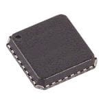
ICGOO电子元器件商城为您提供AD9742ACPZ由Analog设计生产,在icgoo商城现货销售,并且可以通过原厂、代理商等渠道进行代购。 AD9742ACPZ价格参考。AnalogAD9742ACPZ封装/规格:数据采集 - 数模转换器, 12 位 数模转换器 1 32-LFCSP-WQ(5x5)。您可以下载AD9742ACPZ参考资料、Datasheet数据手册功能说明书,资料中有AD9742ACPZ 详细功能的应用电路图电压和使用方法及教程。
AD9742ACPZ 是由 Analog Devices Inc.(现为 Analog Devices, Inc., ADI)生产的一款高性能数模转换器(DAC),属于数据采集系统中的关键组件。该型号的 DAC 主要用于需要高精度、高速度和低功耗的应用场景,适用于多种工业、通信和医疗设备。

 应用场景:

1. 通信系统:
   - 无线基站:AD9742ACPZ 可用于无线通信基础设施中的发射机部分,将数字信号转换为模拟信号,以驱动射频(RF)前端。其高分辨率和快速转换速度使得它特别适合于多载波调制和复杂的调制方案。
   - 软件定义无线电(SDR):在 SDR 系统中,DAC 用于生成各种频率的信号,支持灵活的频谱配置和多模式操作。

2. 测试与测量设备:
   - 任意波形发生器(AWG):AD9742ACPZ 的高分辨率和线性度使其成为 AWG 的理想选择,能够生成精确的复杂波形,满足实验室和研发环境的需求。
   - 示波器:在高端示波器中,DAC 被用于生成参考信号或用于触发和同步功能。

3. 工业自动化:
   - 运动控制系统:在伺服电机和其他精密运动控制应用中,DAC 用于将数字指令转换为模拟电压或电流,以精确控制电机的速度和位置。
   - 过程控制:用于工业自动化中的传感器接口和执行器控制,确保系统的稳定性和响应速度。

4. 医疗设备:
   - 超声成像:在超声设备中,DAC 用于生成高频脉冲信号,驱动超声换能器,从而实现高分辨率的医学成像。
   - 患者监护仪:用于生成生理信号的模拟输出,如心电图(ECG)、血压等,提供准确的监测数据。

5. 音频处理:
   - 专业音频设备:在高端音频系统中,DAC 用于将数字音频信号转换为模拟信号,确保音质的保真度和清晰度。

总之,AD9742ACPZ 凭借其卓越的性能和可靠性,在多个领域中发挥着重要作用,特别是在需要高精度和实时信号处理的应用中。
| 参数 | 数值 |
| 产品目录 | 集成电路 (IC)半导体 |
| 描述 | IC DAC 12BIT 210MSPS 32LFCSP数模转换器- DAC 12-Bit 210 MSPS |
| DevelopmentKit | AD9742ACP-PCBZ |
| 产品分类 | |
| 品牌 | Analog Devices Inc |
| 产品手册 | |
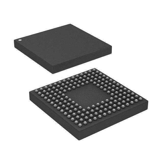
| 产品图片 |
|
| rohs | 符合RoHS无铅 / 符合限制有害物质指令(RoHS)规范要求 |
| 产品系列 | 数据转换器IC,数模转换器- DAC,Analog Devices AD9742ACPZTxDAC® |
| 数据手册 | |
| 产品型号 | AD9742ACPZ |
| 产品培训模块 | http://www.digikey.cn/PTM/IndividualPTM.page?site=cn&lang=zhs&ptm=19145http://www.digikey.cn/PTM/IndividualPTM.page?site=cn&lang=zhs&ptm=18614http://www.digikey.cn/PTM/IndividualPTM.page?site=cn&lang=zhs&ptm=26125http://www.digikey.cn/PTM/IndividualPTM.page?site=cn&lang=zhs&ptm=26140http://www.digikey.cn/PTM/IndividualPTM.page?site=cn&lang=zhs&ptm=26150http://www.digikey.cn/PTM/IndividualPTM.page?site=cn&lang=zhs&ptm=26147 |
| 产品种类 | 数模转换器- DAC |
| 位数 | 12 |
| 供应商器件封装 | 32-LFCSP-VQ(5x5) |
| 分辨率 | 12 bit |
| 包装 | 托盘 |
| 商标 | Analog Devices |
| 安装类型 | 表面贴装 |
| 安装风格 | SMD/SMT |
| 封装 | Tray |
| 封装/外壳 | 32-VFQFN 裸露焊盘,CSP |
| 封装/箱体 | LFCSP-32 |
| 工作温度 | -40°C ~ 85°C |
| 工厂包装数量 | 490 |
| 建立时间 | 11ns |
| 接口类型 | Parallel |
| 数据接口 | 并联 |
| 最大功率耗散 | 145 mW |
| 最大工作温度 | + 85 C |
| 最小工作温度 | - 40 C |
| 标准包装 | 1 |
| 电压参考 | Internal, External |
| 电压源 | 模拟和数字 |
| 电源电压-最大 | 3.6 V |
| 电源电压-最小 | 2.7 V |
| 积分非线性 | +/- 2.5 LSB |
| 稳定时间 | 11 ns |
| 系列 | AD9742 |
| 结构 | Segment |
| 转换器数 | 1 |
| 转换器数量 | 1 |
| 输出数和类型 | 2 电流,单极2 电流,双极 |
| 输出类型 | Current |
| 配用 | /product-detail/zh/AD9742ACP-PCBZ/AD9742ACP-PCBZ-ND/1873563 |
| 采样比 | 210 MSPs |
| 采样率(每秒) | 210M |


- 商务部:美国ITC正式对集成电路等产品启动337调查
- 曝三星4nm工艺存在良率问题 高通将骁龙8 Gen1或转产台积电
- 太阳诱电将投资9.5亿元在常州建新厂生产MLCC 预计2023年完工
- 英特尔发布欧洲新工厂建设计划 深化IDM 2.0 战略
- 台积电先进制程称霸业界 有大客户加持明年业绩稳了
- 达到5530亿美元!SIA预计今年全球半导体销售额将创下新高
- 英特尔拟将自动驾驶子公司Mobileye上市 估值或超500亿美元
- 三星加码芯片和SET,合并消费电子和移动部门,撤换高东真等 CEO
- 三星电子宣布重大人事变动 还合并消费电子和移动部门
- 海关总署:前11个月进口集成电路产品价值2.52万亿元 增长14.8%


PDF Datasheet 数据手册内容提取
12-Bit, 210 MSPS TxDAC Digital-to-Analog Converter Data Sheet AD9742 FEATURES FUNCTIONAL BLOCK DIAGRAM High performance member of pin-compatible TxDAC 3.3V product family Excellent spurious-free dynamic range performance REFLO 150pF AVDD ACOM 1.2V REF SNR at 5 MHz output, 125 MSPS: 70 dB 0.1µF REFIO CURRENT AD9742 Twos complement or straight binary data format FS ADJ SOURCE Differential current outputs: 2 mA to 20 mA ARRAY RSET 3.3V DVDD IOUTA Power dissipation: 135 mW at 3.3 V SEGMENTED LSB Power-down mode: 15 mW at 3.3 V DCOM SWITCHES SWITCHES IOUTB CLOCK On-chip 1.2 V Reference CLOCK LATCHES MODE C28M-OleSa dco SmOpICa,t 2ib8l-ele daidg iTtSalS iOnPte, arfnadc e3 2-lead LFCSP SLEEP DIGITAL DATA INPUTS (DB11–DB0) 02913-B-001 Edge-triggered latches Figure 1. APPLICATIONS Wideband communication transmit channel: Direct IF Base stations Wireless local loops Digital radio links Direct digital synthesis (DDS) Instrumentation GENERAL DESCRIPTION The AD97421 is a 12-bit resolution, wideband, third generation Edge-triggered input latches and a 1.2 V temperature compensated member of the TxDAC series of high performance, low power band gap reference have been integrated to provide a complete CMOS digital-to-analog converters (DACs). The TxDAC family, monolithic DAC solution. The digital inputs support 3 V CMOS consisting of pin-compatible 8-, 10-, 12-, and 14-bit DACs, logic families. is specifically optimized for the transmit signal path of PRODUCT HIGHLIGHTS communication systems. All of the devices share the same interface options, small outline package, and pinout, providing an upward 1. The AD9742 is the 12-bit member of the pin-compatible or downward component selection path based on performance, TxDAC family, which offers excellent INL and DNL resolution, and cost. The AD9742 offers exceptional ac and dc performance. performance while supporting update rates up to 210 MSPS. 2. Data input supports twos complement or straight binary data coding. The AD9742’s low power dissipation makes it well suited for 3. High speed, single-ended CMOS clock input supports portable and low power applications. Its power dissipation can 210 MSPS conversion rate. be further reduced to a mere 60 mW with a slight degradation 4. Low power: Complete CMOS DAC function operates on in performance by lowering the full-scale current output. Also, 135 mW from a 2.7 V to 3.6 V single supply. The DAC full- a power-down mode reduces the standby power dissipation to scale current can be reduced for lower power operation, approximately 15 mW. A segmented current source architecture and a sleep mode is provided for low power idle periods. is combined with a proprietary switching technique to reduce 5. On-chip voltage reference: The AD9742 includes a 1.2 V spurious components and enhance dynamic performance. temperature compensated band gap voltage reference. 6. Industry-standard 28-lead SOIC, 28-lead TSSOP, and 32-lead LFCSP packages. 1 Protected by U.S. Patent Numbers: 5,568,145; 5,689,257; and 5,703,519. Rev. C Document Feedback Information furnished by Analog Devices is believed to be accurate and reliable. However, no responsibility is assumed by Analog Devices for its use, nor for any infringements of patents or other One Technology Way, P.O. Box 9106, Norwood, MA 02062-9106, U.S.A. rights of third parties that may result from its use. Specifications subject to change without notice. No license is granted by implication or otherwise under any patent or patent rights of Analog Devices. Tel: 781.329.4700 ©2002–2013 Analog Devices, Inc. All rights reserved. Trademarks and registered trademarks are the property of their respective owners. Technical Support www.analog.com
AD9742 Data Sheet TABLE OF CONTENTS Features .............................................................................................. 1 Reference Control Amplifier .................................................... 13 Applications ....................................................................................... 1 DAC Transfer Function ............................................................. 13 Functional Block Diagram .............................................................. 1 Analog Outputs .......................................................................... 13 General Description ......................................................................... 1 Digital Inputs .............................................................................. 14 Product Highlights ........................................................................... 1 Clock Input.................................................................................. 14 Revision History ............................................................................... 2 DAC Timing ................................................................................ 15 Specifications ..................................................................................... 3 Power Dissipation....................................................................... 15 DC Specifications ......................................................................... 3 Applying the AD9742 ................................................................ 16 Dynamic Specifications ............................................................... 4 Differential Coupling Using a Transformer ............................... 16 Digital Specifications ................................................................... 5 Differential Coupling Using an Op Amp ................................ 16 Absolute Maximum Ratings ............................................................ 6 Single-Ended, Unbuffered Voltage Output ............................. 17 Thermal Resistance ...................................................................... 6 Single-Ended, Buffered Voltage Output Configuration ........ 17 ESD Caution .................................................................................. 6 Power and Grounding Considerations, Power Supply Pin Configurations and Function Descriptions ........................... 7 Rejection ...................................................................................... 17 Typical Performance Characteristics ............................................. 8 Evaluation Board ............................................................................ 19 Terminology .................................................................................... 11 General Description ................................................................... 19 Functional Description .................................................................. 12 Outline Dimensions ....................................................................... 29 Reference Operation .................................................................. 12 Ordering Guide .......................................................................... 30 REVISION HISTORY 2/13—Rev. B to Rev. C 5/03—Rev. 0 to Rev. A Updated Format .................................................................. Universal Added 32-Lead LFCSP Package ....................................... Universal Changes to Figure 4 and Table 6 ..................................................... 7 Edits to Features and Product Highlights ...................................... 1 Moved Terminology Section ......................................................... 11 Edits to DC Specifications ................................................................ 2 Updated Outline Dimensions ....................................................... 29 Edits to Dynamic Specifications ...................................................... 3 Changes to Ordering Guide .......................................................... 30 Edits to Digital Specifications .......................................................... 4 Edits to Absolute Maximum Ratings, Thermal Characteristics, 6/04—Rev. A to Rev. B and Ordering Guide .......................................................................... 5 Changes to the Title, General Description, and Product Edits to Pin Configuration and Pin Function Descriptions ........ 6 Highlights .......................................................................................... 1 Edits to Figure 2 ................................................................................. 7 Changes to Dynamic Specifications ............................................... 4 Replaced TPCs 1, 4, 7, and 8 ............................................................ 8 Changes to Figure 6 and Figure 10 ................................................. 9 Edits to Figure 3 and Functional Description Section .............. 10 Changes to Figure 12 to Figure 15 ................................................ 10 Added Clock Input Section and Figure 7 .................................... 12 Changes to the Functional Description Section ......................... 12 Edits to DAC Timing Section ....................................................... 12 Changes to the Digital Inputs Section ......................................... 14 Edits to Sleep Mode Operation Section and Power Dissipation Changes to Figure 29 ...................................................................... 15 Section .............................................................................................. 13 Changes to Figure 30 ...................................................................... 16 Renumbered Figure 8 to Figure 26............................................... 13 Added Figure 11 ............................................................................. 13 Added Figure 27 to Figure 35 ....................................................... 21 Updated Outline Dimensions ....................................................... 26 5/02—Revision 0: Initial Version Rev. C | Page 2 of 32
Data Sheet AD9742 SPECIFICATIONS DC SPECIFICATIONS T to T , AVDD = 3.3 V, DVDD = 3.3 V, CLKVDD = 3.3 V, I = 20 mA, unless otherwise noted. MIN MAX OUTFS Table 1. Parameter Min Typ Max Unit RESOLUTION 12 Bits DC ACCURACY1 Integral Linearity Error (INL) −2.5 ±0.5 +2.5 LSB Differential Nonlinearity (DNL) −1.3 ±0.4 +1.3 LSB ANALOG OUTPUT Offset Error −0.02 +0.02 % of FSR Gain Error (Without Internal Reference) −0.5 ±0.1 +0.5 % of FSR Gain Error (With Internal Reference) −0.5 ±0.1 +0.5 % of FSR Full-Scale Output Current2 2 20 mA Output Compliance Range −1 +1.25 V Output Resistance 100 kΩ Output Capacitance 5 pF REFERENCE OUTPUT Reference Voltage 1.14 1.20 1.26 V Reference Output Current3 100 nA REFERENCE INPUT Input Compliance Range 0.1 1.25 V Reference Input Resistance (Ext. Reference) 1 MΩ Small Signal Bandwidth 0.5 MHz TEMPERATURE COEFFICIENTS Offset Drift 0 ppm of FSR/°C Gain Drift (Without Internal Reference) ±50 ppm of FSR/°C Gain Drift (With Internal Reference) ±100 ppm of FSR/°C Reference Voltage Drift ±50 ppm/°C POWER SUPPLY Supply Voltages AVDD 2.7 3.3 3.6 V DVDD 2.7 3.3 3.6 V CLKVDD 2.7 3.3 3.6 V Analog Supply Current (I ) 33 36 mA AVDD Digital Supply Current (I )4 8 9 mA DVDD Clock Supply Current (I ) 5 6 mA CLKVDD Supply Current Sleep Mode (I ) 5 6 mA AVDD Power Dissipation4 135 145 mW Power Dissipation5 145 mW Power Supply Rejection Ratio—AVDD6 −1 +1 % of FSR/V Power Supply Rejection Ratio—DVDD6 −0.04 +0.04 % of FSR/V OPERATING RANGE −40 +85 °C 1 Measured at IOUTA, driving a virtual ground. 2 Nominal full-scale current, IOUTFS, is 32 times the IREF current. 3 An external buffer amplifier with input bias current <100 nA should be used to drive any external load. 4 Measured at fCLOCK = 25 MSPS and fOUT = 1 MHz. 5 Measured as unbuffered voltage output with IOUTFS = 20 mA and 50 Ω RLOAD at IOUTA and IOUTB, fCLOCK = 100 MSPS and fOUT = 40 MHz. 6 ±5% power supply variation. Rev. C | Page 3 of 32
AD9742 Data Sheet DYNAMIC SPECIFICATIONS T to T , AVDD = 3.3 V, DVDD = 3.3 V, CLKVDD = 3.3 V, I = 20 mA, differential transformer coupled output, 50 Ω doubly MIN MAX OUTFS terminated, unless otherwise noted. Table 2. Parameter Min Typ Max Unit DYNAMIC PERFORMANCE Maximum Output Update Rate (f ) 210 MSPS CLOCK Output Settling Time (t ) (to 0.1%)1 11 ns ST Output Propagation Delay (t ) 1 ns PD Glitch Impulse 5 pV-sec Output Rise Time (10% to 90%)1 2.5 ns Output Fall Time (10% to 90%)1 2.5 ns Output Noise (I = 20 mA)2 50 pA/√Hz OUTFS Output Noise (I = 2 mA)2 30 pA/√Hz OUTFS Noise Spectral Density3 −152 dBm/Hz AC LINEARITY Spurious-Free Dynamic Range to Nyquist f = 25 MSPS; f = 1.00 MHz CLOCK OUT 0 dBFS Output 74 84 dBc −6 dBFS Output 85 dBc −12 dBFS Output 82 dBc −18 dBFS Output 76 dBc f = 65 MSPS; f = 1.00 MHz 85 dBc CLOCK OUT f = 65 MSPS; f = 2.51 MHz 83 dBc CLOCK OUT f = 65 MSPS; f = 10 MHz 80 dBc CLOCK OUT f = 65 MSPS; f = 15 MHz 75 dBc CLOCK OUT f = 65 MSPS; f = 25 MHz 74 dBc CLOCK OUT f = 165 MSPS; f = 21 MHz 72 dBc CLOCK OUT f = 165 MSPS; f = 41 MHz 60 dBc CLOCK OUT f = 210 MSPS; f = 40 MHz 67 dBc CLOCK OUT f = 210 MSPS; f = 69 MHz 60 dBc CLOCK OUT Spurious-Free Dynamic Range within a Window f = 25 MSPS; f = 1.00 MHz; 2 MHz Span 80 dBc CLOCK OUT f = 50 MSPS; f = 5.02 MHz; 2 MHz Span 90 dBc CLOCK OUT f = 65 MSPS; f = 5.03 MHz; 2.5 MHz Span 90 dBc CLOCK OUT f = 125 MSPS; f = 5.04 MHz; 4 MHz Span 90 dBc CLOCK OUT Total Harmonic Distortion f = 25 MSPS; f = 1.00 MHz −82 −74 dBc CLOCK OUT f = 50 MSPS; f = 2.00 MHz −77 dBc CLOCK OUT f = 65 MSPS; f = 2.00 MHz −77 dBc CLOCK OUT f = 125 MSPS; f = 2.00 MHz −77 dBc CLOCK OUT Signal-to-Noise Ratio f = 65 MSPS; f = 5 MHz; I = 20 mA 78 dB CLOCK OUT OUTFS f = 65 MSPS; f = 5 MHz; I = 5 mA 86 dB CLOCK OUT OUTFS f = 125 MSPS; f = 5 MHz; I = 20 mA 73 dB CLOCK OUT OUTFS f = 125 MSPS; f = 5 MHz; I = 5 mA 78 dB CLOCK OUT OUTFS f = 165 MSPS; f = 5 MHz; I = 20 mA 69 dB CLOCK OUT OUTFS f = 165 MSPS; f = 5 MHz; I = 5 mA 71 dB CLOCK OUT OUTFS f = 210 MSPS; f = 5 MHz; I = 20 mA 69 dB CLOCK OUT OUTFS f = 210 MSPS; f = 5 MHz; I = 5 mA 66 dB CLOCK OUT OUTFS Rev. C | Page 4 of 32
Data Sheet AD9742 Parameter Min Typ Max Unit Multitone Power Ratio (8 Tones at 400 kHz Spacing) f = 78 MSPS; f = 15.0 MHz to 18.2 MHz CLOCK OUT 0 dBFS Output 65 dBc −6 dBFS Output 67 dBc −12 dBFS Output 65 dBc −18 dBFS Output 63 dBc 1 Measured single-ended into 50 Ω load. 2 Output noise is measured with a full-scale output set to 20 mA with no conversion activity. It is a measure of the thermal noise only. 3 Noise spectral density is the average noise power normalized to a 1 Hz bandwidth, with the DAC converting and producing an output tone. DIGITAL SPECIFICATIONS T to T , AVDD = 3.3 V, DVDD = 3.3 V, CLKVDD = 3.3 V, I = 20 mA, unless otherwise noted. MIN MAX OUTFS Table 3. Parameter Min Typ Max Unit DIGITAL INPUTS1 Logic 1 Voltage 2.1 3 V Logic 0 Voltage 0 0.9 V Logic 1 Current −10 +10 µA Logic 0 Current −10 +10 µA Input Capacitance 5 pF Input Setup Time (t) 2.0 ns S Input Hold Time (t ) 1.5 ns H Latch Pulse Width (t ) 1.5 ns LPW CLK INPUTS2 Input Voltage Range 0 3 V Common-Mode Voltage 0.75 1.5 2.25 V Differential Voltage 0.5 1.5 V 1 Includes CLOCK pin on SOIC/TSSOP packages and CLK+ pin on LFCSP package in single-ended clock input mode. 2 Applicable to CLK+ and CLK− inputs when configured for differential or PECL clock input mode. DB0–DB11 tS tH CLOCK tLPW tPD tST IOUTA IOUOTRB 0.1% 0.1% 02912-B-002 Figure 2. Timing Diagram Rev. C | Page 5 of 32
AD9742 Data Sheet ABSOLUTE MAXIMUM RATINGS THERMAL RESISTANCE Table 4. Thermal impedance measurements were taken on a 4-layer With Parameter Respect to Min Max Unit board in still air, in accordance with EIA/JESD51-7. AVDD ACOM −0.3 +3.9 V Table 5. Thermal Resistance DVDD DCOM −0.3 +3.9 V Package Type θ Unit CLKVDD CLKCOM −0.3 +3.9 V JA ACOM DCOM −0.3 +0.3 V 28-Lead SOIC 55.9 °C/W ACOM CLKCOM −0.3 +0.3 V 28-Lead TSSOP 67.7 °C/W DCOM CLKCOM −0.3 +0.3 V 32-Lead LFCSP 32.5 °C/W AVDD DVDD −3.9 +3.9 V AVDD CLKVDD −3.9 +3.9 V ESD CAUTION DVDD CLKVDD −3.9 +3.9 V CLOCK, SLEEP DCOM −0.3 DVDD + 0.3 V Digital Inputs, MODE DCOM −0.3 DVDD + 0.3 V IOUTA, IOUTB ACOM −1.0 AVDD + 0.3 V REFIO, REFLO, FS ADJ ACOM −0.3 AVDD + 0.3 V CLK+, CLK−, MODE CLKCOM −0.3 CLKVDD + 0.3 V Junction Temperature 150 °C Storage Temperature −65 +150 °C Lead Temperature 300 °C (10 sec) Stresses above those listed under Absolute Maximum Ratings may cause permanent damage to the device. This is a stress rating only; functional operation of the device at these or any other conditions above those indicated in the operational section of this specification is not implied. Exposure to absolute maximum rating conditions for extended periods may affect device reliability. Rev. C | Page 6 of 32
Data Sheet AD9742 PIN CONFIGURATIONS AND FUNCTION DESCRIPTIONS B) (MSB) DB11 1 28 CLOCK MS DB10 2 27 DVDD 67891011 (OMEEP BBBBBBCL DB9 3 26 DCOM DDDDDDDS 2 1 0 9 8 7 6 5 DB8 4 25 MODE 33322222 DB7 5 24 AVDD AD9742 DB5 1 PIN 1 24 FS ADJ DB6 6 23 RESERVED DB4 2 INDICATOR 23 REFIO TOP VIEW DVDD 3 22 ACOM DB5 7 (Not to Scale)22 IOUTA DB3 4 AD9742 21 IOUTA DB4 8 21 IOUTB DB2 5 TOP VIEW 20 IOUTB DB1 6 (Not to Scale) 19 ACOM DB3 9 20 ACOM (LSB) DB0 7 18 AVDD DB2 10 19 NC NC 8 17 AVDD DB1 11 18 FS ADJ 90123456 (LSB) DB0 12 17 REFIO C M 1D 1+ 1– 1M 1E 1E 1 NNCC 11N43C = NO CONNEC1165TRSLEEFELOP 02912-B-003 NOTES NDCOCLKVDCLKCLKCLKCOCMODMOD 1. NC = NO CONNECT. 2. IT IS RECOMMENDED THAT THE EXPOSEDPAD AGBNERD OT UHTHNEERDRM PMALALALLNY EP C EFORONFRNO EERNCMHTAEANDNCCTEEO.D A E CLOECPPTRERICAL 02912-004 Figure 3. 28-Lead SOIC and 28-Lead TSSOP Pin Configuration Figure 4. 32-Lead LFCSP Pin Configuration Table 6. Pin Function Descriptions (N/A = Not Applicable) SOIC/TSSOP LFCSP Pin No. Pin No. Mnemonic Description 1 27 DB11 Most Significant Data Bit (MSB). 2 to 11 28 to 32, DB10 to DB1 Data Bits 10 to 1. 1, 2, 4 to 6 12 7 DB0 Least Significant Data Bit (LSB). 13, 14 8, 9 NC No Internal Connection. 15 25 SLEEP Power-Down Control Input. Active high. Contains active pull-down circuit; it may be left unterminated if not used. 16 N/A REFLO Reference Ground when Internal 1.2 V Reference Used. Connect to AVDD to disable internal reference. 17 23 REFIO Reference Input/Output. Serves as reference input when internal reference disabled (that is, tie REFLO to AVDD). Serves as 1.2 V reference output when internal reference activated (that is, tie REFLO to ACOM). Requires 0.1 µF capacitor to ACOM when internal reference activated. 18 24 FS ADJ Full-Scale Current Output Adjust. 19 N/A NC No Internal Connection. 20 19, 22 ACOM Analog Common. 21 20 IOUTB Complementary DAC Current Output. Full-scale current when all data bits are 0s. 22 21 IOUTA DAC Current Output. Full-scale current when all data bits are 1s. 23 N/A RESERVED Reserved. Do not connect to common or supply. 24 17, 18 AVDD Analog Supply Voltage (3.3 V). 25 16 MODE Selects Input Data Format. Connect to DCOM for straight binary, DVDD for twos complement. N/A 15 CMODE Clock Mode Selection. Connect to CLKCOM for single-ended clock receiver (drive CLK+ and float CLK–). Connect to CLKVDD for differential receiver. Float for PECL receiver (terminations on-chip). 26 10, 26 DCOM Digital Common. 27 3 DVDD Digital Supply Voltage (3.3 V). 28 N/A CLOCK Clock Input. Data latched on positive edge of clock. N/A 12 CLK+ Differential Clock Input. N/A 13 CLK− Differential Clock Input. N/A 11 CLKVDD Clock Supply Voltage (3.3 V). N/A 14 CLKCOM Clock Common. N/A EPAD It is recommended that the exposed pad be thermally connected to a copper ground plane for enhanced electric and thermal performance. Rev. C | Page 7 of 32
AD9742 Data Sheet TYPICAL PERFORMANCE CHARACTERISTICS 95 95 125MSPS 90 210MSPS (LFCSP) 90 0dBFS 85 165MSPS (LFCSP) 85 –6dBFS (LFCSP) 80 65MSPS 80 c) 75 c) 75 dB 210MSPS dB –12dBFS R ( 70 165MSPS R ( 70 D D F F S 65 S 65 125MSPS (LFCSP) –12dBFS (LFCSP) 60 60 0dBFS (LFCSP) –6dBFS 55 55 50 50 451 fOUT1 (0MHz) 100 02912-B-006 450 10 20 fOUT3 (0MHz) 40 50 60 02912-B-007 Figure 5. SFDR vs. fOUT @ 0 dBFS Figure 8. SFDR vs. fOUT @ 165 MSPS 95 95 90 90 85 0dBFS (LFCSP) 85 80 0dBFS 80 –12dBFS Bc) 75 c) 75 DR (d 70 –6dBFS R (dB 70 –6dBFS (LFCSP) –6dBFS F D S 65 F S 65 60 –12dBFS 60 55 55 –12dBFS (LFCSP) 50 50 0dBFS 450 5 10fOUT (MHz)15 20 25 02912-B-009 450 10 20 3fO0UT (MH4z0) 50 60 70 02912-B-054 Figure 6. SFDR vs. fOUT @ 65 MSPS Figure 9. SFDR vs. fOUT @ 210 MSPS 95 95 90 90 85 85 80 80 20mA c) 75 c) 75 B B R (d 70 –6dBFS R (d 70 10mA D D SF 65 –12dBFS SF 65 5mA 60 0dBFS 60 55 55 50 50 450 5 10 15 f2O0UT (MH25z) 30 35 40 45 02912-B-012 450 5 10fOUT (MHz)15 20 25 02912-B-010 Figure 7. SFDR vs. fOUT @ 125 MSPS Figure 10. SFDR vs. fOUT and IOUTFS @ 65 MSPS and 0 dBFS Rev. C | Page 8 of 32
Data Sheet AD9742 95 95 90 90 78MSPS (10.1,12.1) 85 85 65MSPS (8.3,10.3) 65MSPS 80 80 125MSPS Bc) 75 c) 75 125MSPS (16.9, 18.9) d 165MSPS B DR ( 70 R (d 70 210MSPS (29, 31) F D S 65 210MSPS SF 65 165MSPS (22.6, 24.6) 210MSPS (29, 31) 60 210MSPS (LFCSP) 60 55 55 50 50 45–25 –20 –1A5OUT (dBFS–1)0 –5 0 02912-B-013 45–25 –20 –1A5OUT (dBFS–1)0 –5 0 02912-B-014 Figure 11. Single-Tone SFDR vs. AOUT @ fOUT = fCLOCK/11 Figure 14. Dual-Tone IMD vs. AOUT @ fOUT = fCLOCK/7 95 1.0 90 85 125MSPS (LFCSP) 0.5 65MSPS 80 SFDR (dBc) 677505 165MSPS (LFCSP) ERROR (LSB) 0 165MSPS 60 125MSPS –0.5 55 210MSPS (LFCSP) 50 210MSPS 45–25 –20 –1A5OUT (dBFS–1)0 –5 0 02912-B-008 –1.00 1024 C2O04D8E 3072 4096 02912-B-015 Figure 12. Single-Tone SFDR vs. AOUT @ fOUT = fCLOCK/5 Figure 15. Typical INL 80 1.0 0.8 75 20mA 0.6 70 0.4 SB) 0.2 R L SN 65 5mA 10mA ROR ( 0 R –0.2 E 60 –0.4 55 –0.6 –0.8 5025 45 65 85 fC10LO5CK (1M25Hz) 145 165 185 205 02912-B-011 –1.00 1024 C2O04D8E 3072 4096 02912-B-017 Figure 13. SNR vs. fCLOCK and IOUTFS @ fOUT = 5 MHz and 0 dBFS Figure 16. Typical DNL Rev. C | Page 9 of 32
AD9742 Data Sheet 90 0 –10 fCLOCK = 78MSPS 85 fOUT1 = 15.0MHz 4MHz –20 fOUT2 = 15.4MHz 80 SFDR = 77dBc –30 AMPLITUDE = 0dBFS m) 75 B SFDR (dBc) 6750 19MHz AGNITUDE (d –––654000 49MHz M –70 60 34MHz –80 55 –90 50–40 –20 0TEMPERA20TURE (°C4)0 60 80 02912-B-019 –1001 6 11 FRE1Q6UENCY 2(1MHz) 26 31 36 02912-B-018 Figure 17. SFDR vs. Temperature @ 165 MSPS, 0 dBFS Figure 19. Dual-Tone SFDR 0 0 –10 ffCOLUOTC =K 1 =5 .708MMHSzPS –10 ffCOLUOTC1 K= =1 57.80MMSHPzS SFDR = 79dBc –20 AMPLITUDE = 0dBFS –20 fOUT2 = 15.4MHz –30 –30 fOUT3 = 15.8MHz Bm) Bm) fOUT4 = 16.2MHz d –40 d –40 E ( E ( SFDR = 75dBc UD –50 UD –50 AMPLITUDE = 0dBFS T T NI NI G –60 G –60 A A M M –70 –70 –80 –80 –90 –90 –1001 6 11 FRE1Q6UENCY2 (1MHz) 26 31 36 02912-B-016 –1001 6 11 FRE1Q6UENCY2 (1MHz) 26 31 36 02912-B-020 Figure 18. Single-Tone SFDR Figure 20. Four-Tone SFDR 3.3V REFLO 150pF AVDD ACOM 1.2V REF AD9742 VREFIO REFIO PMOS 0.1µF IREF FS ADJ CURRENT SOURCE RSET ARRAY VDIFF= VOUTA– VOUTB 2kΩ 3.3V DVDD IOUTA IOUTA DCOM SEGMFOERN TDEBD1 1S–WDIBT3CHES SWLITSCBHES IOUTB IOUTB VOUTB VROLOUATAD CLOCK CLOCK LATCHES MODE RLOAD 50Ω SLEEP DIGITAL DATA INPUTS (DB11–DB0) 50Ω 02912-B-021 Figure 21. Simplified Block Diagram (SOIC/TSSOP Packages) Rev. C | Page 10 of 32
Data Sheet AD9742 TERMINOLOGY Power Supply Rejection Linearity Error (Also Called Integral Nonlinearity or INL) The maximum change in the full-scale output as the supplies Linearity error is defined as the maximum deviation of the are varied from nominal to minimum and maximum specified actual analog output from the ideal output, determined by a voltages. straight line drawn from zero to full scale. Settling Time Differential Nonlinearity (or DNL) The time required for the output to reach and remain within a DNL is the measure of the variation in analog value, normalized specified error band about its final value, measured from the to full scale, associated with a 1 LSB change in digital input start of the output transition. code. Glitch Impulse Monotonicity Asymmetrical switching times in a DAC give rise to undesired A DAC is monotonic if the output either increases or remains output transients that are quantified by a glitch impulse. It is constant as the digital input increases. specified as the net area of the glitch in pV-s. Offset Error Spurious-Free Dynamic Range The deviation of the output current from the ideal of zero is The difference, in dB, between the rms amplitude of the output called the offset error. For IOUTA, 0 mA output is expected signal and the peak spurious signal over the specified when the inputs are all 0s. For IOUTB, 0 mA output is expected bandwidth. when all inputs are set to 1s. Total Harmonic Distortion (THD) Gain Error THD is the ratio of the rms sum of the first six harmonic The difference between the actual and ideal output span. The components to the rms value of the measured input signal. It is actual span is determined by the output when all inputs are set expressed as a percentage or in decibels (dB). to 1s minus the output when all inputs are set to 0s. Multitone Power Ratio Output Compliance Range The spurious-free dynamic range containing multiple carrier The range of allowable voltage at the output of a current output tones of equal amplitude. It is measured as the difference DAC. Operation beyond the maximum compliance limits may between the rms amplitude of a carrier tone to the peak cause either output stage saturation or breakdown, resulting in spurious signal in the region of a removed tone. nonlinear performance. Temperature Drift Temperature drift is specified as the maximum change from the ambient (25°C) value to the value at either T or T . For MIN MAX offset and gain drift, the drift is reported in ppm of full-scale range (FSR) per °C. For reference drift, the drift is reported in ppm per °C. 3.3V REFLO AVDD ACOM 150pF 1.2V REF AD9742 0.1µF REFIO PMOS FS ADJ CURRENT SOURCE ARRAY MINI-CIRCUITS RSET T1-1T 2kΩ 3.3V DVDD ROHDE & SCHWARZ IOUTA FSEA30 DCOM SEGMFOERN TDEBD1 1S–WDIBTC3HES SWILTSCBHES IOUTB SAPNEACLTYRZEURM CLOCK MODE DDCVODMD 50Ω SLEEP LATCHES 50Ω RETIMED 50Ω CLOCK DIGITAL OUTPUT* DATA PULLSEEC GROENYE 9R2A10TOR OCULTOPCUKT TEKWTRITOHN OIXP ATIWOGN -42021 *STOAROFWA 5TGN0HS%2A0I TT2DI 1OTU HCNTEYLS O DCOCIYNGKC IF TLRAAEELL TCL IDLIMNAOEGTCD AEKD.GE 02912-B-005 Figure 22. Basic AC Characterization Test Set-Up (SOIC/TSSOP Packages) Rev. C | Page 11 of 32
AD9742 Data Sheet FUNCTIONAL DESCRIPTION AD9742 consists of a DAC, digital control logic, and full-scale REFERENCE OPERATION output current control. The DAC contains a PMOS current The AD9742 contains an internal 1.2 V band gap reference. The source array capable of providing up to 20 mA of full-scale internal reference can be disabled by raising REFLO to AVDD. current (I ). The array is divided into 31 equal currents that OUTFS It can also be easily overridden by an external reference with no make up the five most significant bits (MSBs). The next four effect on performance. REFIO serves as either an input or an bits, or middle bits, consist of 15 equal current sources whose output depending on whether the internal or an external value is 1/16th of an MSB current source. The remaining LSBs reference is used. To use the internal reference, simply decouple are binary weighted fractions of the middle bits current sources. the REFIO pin to ACOM with a 0.1 µF capacitor and connect Implementing the middle and lower bits with current sources, REFLO to ACOM via a resistance less than 5 Ω. The internal instead of an R-2R ladder, enhances its dynamic performance reference voltage will be present at REFIO. If the voltage at for multitone or low amplitude signals and helps maintain the REFIO is to be used anywhere else in the circuit, an external DAC’s high output impedance (i.e., >100 kΩ). buffer amplifier with an input bias current of less than 100 nA All of these current sources are switched to one or the other of should be used. An example of the use of the internal reference the two output nodes (i.e., IOUTA or IOUTB) via PMOS is shown in Figure 23. differential current switches. The switches are based on the 3.3V architecture that was pioneered in the AD9764 family, with OPTIONAL EXTERNAL further REF BUFFER REFLO 150pF AVDD refinements to reduce distortion contributed by the switching 1.2V REF transient. This switch architecture also reduces various timing REFIO CURRENT errors and provides matching complementary drive signals to ADDITIOLONAADL 0.1µF FS ADJ SAORURRACYE tThhee i nanpaultosg o af nthde d digififtearle snetcitailo cnusr oref ntht es wAiDtc9h7e4s.2 have separate 2kΩ AD9742 02912-B-022 power supply inputs (i.e., AVDD and DVDD) that can operate Figure 23. Internal Reference Configuration independently over a 2.7 V to 3.6 V range. The digital section, An external reference can be applied to REFIO, as shown in which is capable of operating at a rate of up to 210 MSPS, Figure 24. The external reference may provide either a fixed consists of edge-triggered latches and segment decoding logic reference voltage to enhance accuracy and drift performance or circuitry. The analog section includes the PMOS current a varying reference voltage for gain control. Note that the 0.1 µF sources, the associated differential switches, a 1.2 V band gap compensation capacitor is not required since the internal voltage reference, and a reference control amplifier. reference is overridden, and the relatively high input impedance The DAC full-scale output current is regulated by the reference of REFIO minimizes any loading of the external reference. control amplifier and can be set from 2 mA to 20 mA via an 3.3V external resistor, R , connected to the full-scale adjust (FS SET ADJ) pin. The external resistor, in combination with both the reference control amplifier and voltage reference ,V , sets the REFIO REFLO 150pF AVDD AVDD reference current, IREF, which is replicated to the segmented 1.2V REF current sources with the proper scaling factor. The full-scale EXTERNAL VREFIO REFIO current, IOUTFS, is 32 times IREF. REF FS ADJ CSUORURRECNET ARRAY RSET IREF = VREFIO/RSET AD9742 RCAEOMFNPETLRRIFEOIENLRCE 02912-B-023 Figure 24. External Reference Configuration Rev. C | Page 12 of 32
Data Sheet AD9742 REFERENCE CONTROL AMPLIFIER V =(IOUTA−IOUTB)×R (7) DIFF LOAD The AD9742 contains a control amplifier that is used to regulate Substituting the values of IOUTA, IOUTB, I , and V can be REF DIFF the full-scale output current, IOUTFS. The control amplifier is expressed as: configured as a V-I converter, as shown in Figure 24, so that its {( ) } V = 2×DACCODE−4095 /4096 current output, IREF, is determined by the ratio of the VREFIO and (32DI×FFR /R )×V (8) an external resistor, RSET, as stated in Equation 4. IREF is copied LOAD SET REFIO to the segmented current sources with the proper scale factor to Equations 7 and 8 highlight some of the advantages of operating set IOUTFS, as stated in Equation 3. the AD9742 differentially. First, the differential operation helps The control amplifier allows a wide (10:1) adjustment span of cancel common-mode error sources associated with IOUTA IOUTFS over a 2 mA to 20 mA range by setting IREF between and IOUTB, such as noise, distortion, and dc offsets. Second, 62.5 µA and 625 µA. The wide adjustment span of IOUTFS the differential code-dependent current and subsequent voltage, provides several benefits. The first relates directly to the power VDIFF, is twice the value of the single-ended voltage output (i.e., dissipation of the AD9742, which is proportional to IOUTFS (see VOUTA or VOUTB), thus providing twice the signal power to the load. the Power Dissipation section). The second relates to the 20 dB Note that the gain drift temperature performance for a single- adjustment, which is useful for system gain control purposes. ended (V and V ) or differential output (V ) of the OUTA OUTB DIFF The small signal bandwidth of the reference control amplifier is AD9742 can be enhanced by selecting temperature tracking approximately 500 kHz and can be used for low frequency small resistors for RLOAD and RSET due to their ratiometric relationship, signal multiplying applications. as shown in Equation 8. DAC TRANSFER FUNCTION ANALOG OUTPUTS Both DACs in the AD9742 provide complementary current The complementary current outputs in each DAC, IOUTA, outputs, IOUTA and IOUTB. IOUTA provides a near full-scale and IOUTB may be configured for single-ended or differential current output, I , when all bits are high (i.e., DAC CODE = operation. IOUTA and IOUTB can be converted into comple- OUTFS 4095), while IOUTB, the complementary output, provides no mentary single-ended voltage outputs, VOUTA and VOUTB, via a current. The current output appearing at IOUTA and IOUTB is load resistor, RLOAD, as described in the DAC Transfer Function a function of both the input code and IOUTFS and can be section by Equations 5 through 8. The differential voltage, VDIFF, expressed as: existing between VOUTA and VOUTB, can also be converted to a ( ) single-ended voltage via a transformer or differential amplifier IOUTA= DACCODE/4096 ×I (1) OUTFS configuration. The ac performance of the AD9742 is optimum and ( ) IOUTB= 4095−DACCODE/4096×I (2) specified using a differential transformer-coupled output in which OUTFS the voltage swing at IOUTA and IOUTB is limited to ±0.5 V. where DAC CODE = 0 to 4095 (i.e., decimal representation). The distortion and noise performance of the AD9742 can be As mentioned previously, I is a function of the reference OUTFS enhanced when it is configured for differential operation. The current I , which is nominally set by a reference voltage, REF common-mode error sources of both IOUTA and IOUTB can V , and external resistor, R . It can be expressed as: REFIO SET be significantly reduced by the common-mode rejection of a I =32×I (3) transformer or differential amplifier. These common-mode OUTFS REF error sources include even-order distortion products and noise. where The enhancement in distortion performance becomes more IREF =VREFIO/RSET (4) significant as the frequency content of the reconstructed waveform increases and/or its amplitude decreases. This is due The two current outputs will typically drive a resistive load to the first-order cancellation of various dynamic common- directly or via a transformer. If dc coupling is required, IOUTA mode distortion mechanisms, digital feedthrough, and noise. and IOUTB should be directly connected to matching resistive loads, RLOAD, that are tied to analog common, ACOM. Note that Performing a differential-to-single-ended conversion via a RLOAD may represent the equivalent load resistance seen by transformer also provides the ability to deliver twice the IOUTA or IOUTB as would be the case in a doubly terminated reconstructed signal power to the load (assuming no source 50 Ω or 75 Ω cable. The single-ended voltage output appearing termination). Since the output currents of IOUTA and IOUTB at the IOUTA and IOUTB nodes is simply are complementary, they become additive when processed V =IOUTA×R (5) differentially. A properly selected transformer will allow the OUTA LOAD AD9742 to provide the required power and voltage levels to VOUTB =IOUTB×RLOAD (6) different loads. Note that the full-scale value of VOUTA and VOUTB should not exceed the specified output compliance range to maintain specified distortion and linearity performance. Rev. C | Page 13 of 32
AD9742 Data Sheet The output impedance of IOUTA and IOUTB is determined by CLOCK INPUT the equivalent parallel combination of the PMOS switches SOIC/TSSOP Packages associated with the current sources and is typically 100 kΩ in The 28-lead package options have a single-ended clock input parallel with 5 pF. It is also slightly dependent on the output (CLOCK) that must be driven to rail-to-rail CMOS levels. The voltage (i.e., V and V ) due to the nature of a PMOS OUTA OUTB quality of the DAC output is directly related to the clock quality, device. As a result, maintaining IOUTA and/or IOUTB at a and jitter is a key concern. Any noise or jitter in the clock will virtual ground via an I-V op amp configuration will result in translate directly into the DAC output. Optimal performance the optimum dc linearity. Note that the INL/DNL specifications will be achieved if the CLOCK input has a sharp rising edge, for the AD9742 are measured with IOUTA maintained at a since the DAC latches are positive edge triggered. virtual ground via an op amp. LFCSP Package IOUTA and IOUTB also have a negative and positive voltage compliance range that must be adhered to in order to achieve A configurable clock input is available in the LFCSP package, optimum performance. The negative output compliance range which allows for one single-ended and two differential modes. of −1 V is set by the breakdown limits of the CMOS process. The mode selection is controlled by the CMODE input, as Operation beyond this maximum limit may result in a breakdown summarized in Table 7. Connecting CMODE to CLKCOM of the output stage and affect the reliability of the AD9742. selects the single-ended clock input. In this mode, the CLK+ input is driven with rail-to-rail swings and the CLK− input is The positive output compliance range is slightly dependent on left floating. If CMODE is connected to CLKVDD, the differential the full-scale output current, I . It degrades slightly from its OUTFS receiver mode is selected. In this mode, both inputs are high nominal 1.2 V for an I = 20 mA to 1 V for an I = 2 mA. OUTFS OUTFS impedance. The final mode is selected by floating CMODE. This The optimum distortion performance for a single-ended or mode is also differential, but internal terminations for positive differential output is achieved when the maximum full-scale emitter-coupled logic (PECL) are activated. There is no significant signal at IOUTA and IOUTB does not exceed 0.5 V. performance difference between any of the three clock input modes. DIGITAL INPUTS Table 7. Clock Mode Selection The AD9742 digital section consists of 12 input bit channels CMODE Pin Clock Input Mode and a clock input. The 12-bit parallel data inputs follow standard CLKCOM Single-Ended positive binary coding, where DB11 is the most significant bit CLKVDD Differential (MSB) and DB0 is the least significant bit (LSB). IOUTA produces Float PECL a full-scale output current when all data bits are at Logic 1. IOUTB produces a complementary output with the full-scale current The single-ended input mode operates in the same way as the split between the two outputs as a function of the input code. CLOCK input in the 28-lead packages, as described previously. DVDD In the differential input mode, the clock input functions as a high impedance differential pair. The common-mode level of the CLK+ and CLK− inputs can vary from 0.75 V to 2.25 V, and DIGITAL INPUT the differential voltage can be as low as 0.5 V p-p. This mode 02912-B-024 ctthhaeen hsbiineg ehu swgeaadiv neto bi ndatnroidv awe sitidhntegh lc eolo-fe ctnkhd ewe dditi hfsfq eaur edanrifetfi eawrle ainvnetpi auinlt tsse iwnrneila lwl clyao.v nev seirntc e Figure 25. Equivalent Digital Input The final clock mode allows for a reduced external component The digital interface is implemented using an edge-triggered count when the DAC clock is distributed on the board using master/slave latch. The DAC output updates on the rising edge PECL logic. The internal termination configuration is shown in of the clock and is designed to support a clock rate as high as Figure 26. These termination resistors are untrimmed and can 210 MSPS. The clock can be operated at any duty cycle that meets vary up to ±20%. However, matching between the resistors the specified latch pulse width. The setup and hold times can should generally be better than ±1%. also be varied within the clock cycle as long as the specified minimum times are met, although the location of these AD9742 transition edges may affect digital feedthrough and distortion CLK+ performance. Best performance is typically achieved when the CLK– CRLEOCCEIKVER TO DAC CORE input data transitions on the falling edge of a 50% duty cycle clock. 50Ω 50Ω VTT = 1.3V NOM 02912-B-025 Figure 26. Clock Termination in PECL Mode\ Rev. C | Page 14 of 32
Data Sheet AD9742 DAC TIMING The power dissipation is directly proportional to the analog supply Input Clock and Data Timing Relationship current, IAVDD, and the digital supply current, IDVDD. IAVDD is directly proportional to I , as shown in Figure 28, and is insensitive to OUTFS Dynamic performance in a DAC is dependent on the relationship f . Conversely, I is dependent on both the digital input CLOCK DVDD between the position of the clock edges and the time at which waveform, f , and digital supply DVDD. Figure 29 shows CLOCK the input data changes. The AD9742 is rising edge triggered, I as a function of full-scale sine wave output ratios DVDD and so exhibits dynamic performance sensitivity when the data (f /f ) for various update rates with DVDD = 3.3 V. OUT CLOCK transition is close to this edge. In general, the goal when applying 35 the AD9742 is to make the data transition close to the falling clock edge. This becomes more important as the sample rate 30 increases. Figure 27 shows the relationship of SFDR to clock placement with different sample rates. Note that at the lower 25 sample rates, more tolerance is allowed in clock placement, A) while at higher rates, more care must be taken. m (D20 D 75 AV I 70 15 65 10 60 20MHz SFDR dB55 50MHz SFDR 02 4 6 8 IO1U0TFS (m12A) 14 16 18 20 02912-B-027 50 Figure 28. IAVDD vs. IOUTFS 45 20 18 40 35–350MHz S–F2DR –1 n0s 1 2 3 02912-B-026 A)111642 121605MMSSPPSS Figure 27. SFDR vs. Clock Placement @ fOUT = 20 MHz and 50 MHz m (D10 Sleep Mode Operation DVD 125MSPS I 8 The AD9742 has a power-down function that turns off the 6 output current and reduces the supply current to less than 6 mA over the specified supply range of 2.7 V to 3.6 V and temperature 4 65MSPS range. This mode can be activated by applying a Logic Level 1 2 tAoV tDheD S. LTEhEisP d piginit.a Tl ihnep uSLt aElEsoP c poinnt aloingsic a tnh arecsthivoel dp uisl le-dquowaln to c i0r.c5u Ωit 00.01 RATIO (f0O.U1T/fCLOCK) 1 02912-B-028 that ensures that the AD9742 remains enabled if this input is Figure 29. IDVDD vs. Ratio @ DVDD = 3.3 V left disconnected. The AD9742 takes less than 50 ns to power down and approximately 5 µs to power back up. 12 POWER DISSIPATION 10 The power dissipation, P , of the AD9742 is dependent on several DIFF D factors that include: 8 mA) PECL • The power supply voltages (AVDD, CLKVDD, and DVDD) (D D 6 • The full-scale current output IOUTFS LKV C • The update rate fCLOCK I 4 • The reconstructed digital input waveform SE 2 00 50 1f0C0LOCK (MSP1S50) 200 250 02912-B-029 Figure 30. ICLKVDD vs. fCLOCK and Clock Mode Rev. C | Page 15 of 32
AD9742 Data Sheet APPLYING THE AD9742 termination that results in a low VSWR. Note that approximately Output Configurations half the signal power will be dissipated across RDIFF. DIFFERENTIAL COUPLING USING AN OP AMP The following sections illustrate some typical output configurations for the AD9742. Unless otherwise noted, it is assumed that IOUTFS is An op amp can also be used to perform a differential-to-single- set to a nominal 20 mA. For applications requiring the optimum ended conversion, as shown in Figure 32. The AD9742 is configured dynamic performance, a differential output configuration is with two equal load resistors, R , of 25 Ω. The differential LOAD suggested. A differential output configuration may consist of voltage developed across IOUTA and IOUTB is converted to a either an RF transformer or a differential op amp configuration. single-ended signal via the differential op amp configuration. The transformer configuration provides optimum high frequency An optional capacitor can be installed across IOUTA and IOUTB, performance and is recommended for any application that allows forming a real pole in a low-pass filter. The addition of this ac coupling. The differential op amp configuration is suitable capacitor also enhances the op amp’s distortion performance by for applications requiring dc coupling, a bipolar output, signal preventing the DAC’s high slewing output from overloading the gain, and/or level shifting within the bandwidth of the chosen op amp’s input. op amp. 500Ω A single-ended output is suitable for applications requiring a AD9742 225Ω unipolar voltage output. A positive unipolar output voltage will IOUTA 22 result if IOUTA and/or IOUTB are connected to an appropriately 225Ω AD8047 sized load resistor, R , referred to ACOM. This configuration IOUTB 21 LOAD COPT may be more suitable for a single-supply system requiring a 500Ω admc-pcloifuieprl ecdo,u gldro buen cdo-nrfeifgeurrreedd aosu atnp uI-tV v oclotnagveer. tAerl,t ethrnusa tciovnelvye, ratnin g 25Ω 25Ω 02912-B-031 IOUTA or IOUTB into a negative unipolar voltage. This Figure 32. DC Differential Coupling Using an Op Amp configuration provides the best dc linearity since IOUTA or The common-mode rejection of this configuration is typically IOUTB is maintained at a virtual ground. determined by the resistor matching. In this circuit, the DIFFERENTIAL COUPLING USING A TRANSFORMER differential op amp circuit using the AD8047 is configured to provide some additional signal gain. The op amp must operate An RF transformer can be used to perform a differential-to-single- off a dual supply since its output is approximately ±1 V. A high ended signal conversion, as shown in Figure 31. A differentially speed amplifier capable of preserving the differential performance coupled transformer output provides the optimum distortion of the AD9742 while meeting other system level objectives (e.g., performance for output signals whose spectral content lies within cost or power) should be selected. The op amp’s differential gain, the transformer’s pass band. An RF transformer, such as the gain setting resistor values, and full-scale output swing capabilities Mini-Circuits T1–1T, provides excellent rejection of common- should all be considered when optimizing this circuit. mode distortion (that is, even-order harmonics) and noise over a wide frequency range. It also provides electrical isolation and The differential circuit shown in Figure 33 provides the necessary the ability to deliver twice the power to the load. Transformers with level shifting required in a single-supply system. In this case, different impedance ratios may also be used for impedance matching AVDD, which is the positive analog supply for both the AD9742 purposes. Note that the transformer provides ac coupling only. and the op amp, is also used to level shift the differential output of the AD9742 to midsupply (i.e., AVDD/2). The AD8041 is a MINI-CIRCUITS T1-1T suitable op amp for this application. IOUTA 22 500Ω AD9742 RLOAD AD9742 IOUTB 21 OPTIONAL RDIFF 02912-B-030 IOUTA 22 222255ΩΩ AD8041 Figure 31. Differential Output Using a Transformer IOUTB 21 COPT 1kΩ Tcohnen ceecntetedr ttoa pA oCnO tMhe tpor pimroavriyd sei dthee o nf etchees tsraarnys dfocr cmuerrre mntu psta tbhe 25Ω 25Ω 1kΩ AVDD 02912-B-032 for both IOUTA and IOUTB. The complementary voltages Figure 33. Single-Supply DC Differential Coupled Circuit appearing at IOUTA and IOUTB (i.e., V and V ) swing OUTA OUTB symmetrically around ACOM and should be maintained with the specified output compliance range of the AD9742. A differential resistor, R , may be inserted in applications where the output DIFF of the transformer is connected to the load, R , via a passive LOAD reconstruction filter or cable. R is determined by the DIFF transformer’s impedance ratio and provides the proper source Rev. C | Page 16 of 32
Data Sheet AD9742 SINGLE-ENDED, UNBUFFERED VOLTAGE OUTPUT POWER AND GROUNDING CONSIDERATIONS, POWER SUPPLY REJECTION Figure 34 shows the AD9742 configured to provide a unipolar output range of approximately 0 V to 0.5 V for a doubly terminated Many applications seek high speed and high performance under 50 Ω cable since the nominal full-scale current, IOUTFS, of 20 mA less than ideal operating conditions. In these application circuits, flows through the equivalent RLOAD of 25 Ω. In this case, RLOAD the implementation and construction of the printed circuit represents the equivalent load resistance seen by IOUTA or board is as important as the circuit design. Proper RF techniques IOUTB. The unused output (IOUTA or IOUTB) can be connected must be used for device selection, placement, and routing as to ACOM directly or via a matching RLOAD. Different values of well as power supply bypassing and grounding to ensure IOUTFS and RLOAD can be selected as long as the positive compliance optimum performance. Figure 40 to Figure 43 illustrate the range is adhered to. One additional consideration in this mode recommended printed circuit board ground, power, and signal is the integral nonlinearity (INL), discussed in the Analog Outputs plane layouts implemented on the AD9742 evaluation board. section. For optimum INL performance, the single-ended, buffered One factor that can measurably affect system performance is voltage output configuration is suggested. the ability of the DAC output to reject dc variations or ac noise superimposed on the analog or digital dc power distribution. AD9742 IOUTFS= 20mA VOUTA= 0V TO 0.5V This is referred to as the power supply rejection ratio (PSRR). IOUTA 22 For dc variations of the power supply, the resulting performance 50Ω 50Ω of the DAC directly corresponds to a gain error associated with IOUTB 21 25Ω 02912-B-033 itsh ec oDmAmCo’sn f uinll -aspcpalliec cautirornesn wt, hIOeUrTeF St.h Ae Cp onwoeisre d oisnt rtihbeu tdico nsu ips plies Figure 34. 0 V to 0.5 V Unbuffered Voltage Output generated by a switching power supply. Typically, switching SINGLE-ENDED, BUFFERED VOLTAGE OUTPUT power supply noise will occur over the spectrum from tens of CONFIGURATION kHz to several MHz. The PSRR versus frequency of the AD9742 AVDD supply over this frequency range is shown in Figure 36. Figure 35 shows a buffered single-ended output configuration 85 in which the op amp U1 performs an I-V conversion on the AD9742 output current. U1 maintains IOUTA (or IOUTB) at a 80 virtual ground, minimizing the nonlinear output impedance 75 effect on the DAC’s INL performance as described in the Analog 70 Outputs section. Although this single-ended configuration typically B) provides the best dc linearity performance, its ac distortion R (d65 performance at higher DAC update rates may be limited by U1’s SR60 P slew rate capabilities. U1 provides a negative unipolar output 55 voltage, and its full-scale output voltage is simply the product of 50 R and I . The full-scale output should be set within U1’s FB OUTFS voltage output swing capabilities by scaling IOUTFS and/or RFB. An 45 irmedpurcoevde ImOUeTnFSt siinn caec Udi1s twoirltl iboen rpeqerufiorerdm taon scien km laesys r seisgunlatl wcuitrhr ean t. 400 2 4FREQUEN6CY (MHz)8 10 12 02912-B-035 COPT Figure 36. Power Supply Rejection Ratio (PSRR) RFB Note that the ratio in Figure 36 is calculated as amps out/volts 200Ω in. Noise on the analog power supply has the effect of modulating AD9742 IOUTFS= 10mA the internal switches, and therefore the output current. The IOUTA 22 U1 VOUT= IOUTFS× RFB voltage noise on AVDD, therefore, will be added in a nonlinear IOUTB 21 manner to the desired IOUT. Due to the relative different size of 200Ω 02912-B-034 tah mesiex sinwgit cehffeesc, tt hthe aPt ScRaRn ims voedruyl acoted leo dwe pfreenqdueennt.c Ty hpios wcaenr psuropdpulyc e Figure 35. Unipolar Buffered Voltage Output noise to higher frequencies. Worst-case PSRR for either one of the differential DAC outputs will occur when the full-scale current is directed toward that output. As a result, the PSRR measurement in Figure 36 represents a worst-case condition in which the digital inputs remain static and the full-scale output current of 20 mA is directed to the DAC output being measured. Rev. C | Page 17 of 32
AD9742 Data Sheet An example serves to illustrate the effect of supply noise on the possible. Similarly, DVDD, the digital supply, should be decoupled analog supply. Suppose a switching regulator with a switching to DCOM as close to the chip as physically possible. frequency of 250 kHz produces 10 mV of noise and, for simplicity’s For those applications that require a single 3.3 V supply for both sake (ignoring harmonics), all of this noise is concentrated at the analog and digital supplies, a clean analog supply may be 250 kHz. To calculate how much of this undesired noise will generated using the circuit shown in Figure 37. The circuit consists appear as current noise superimposed on the DAC’s full-scale of a differential LC filter with separate power supply and return current, I , one must determine the PSRR in dB using Figure 36 OUTFS lines. Lower noise can be attained by using low ESR type at 250 kHz. To calculate the PSRR for a given R , such that the LOAD electrolytic and tantalum capacitors. units of PSRR are converted from A/V to V/V, adjust the curve in FERRITE Figure 36 by the scaling factor 20 Ω log (RLOAD). For instance, if BEADS R is 50 Ω, the PSRR is reduced by 34 dB (i.e., PSRR of the DAC TTL/CMOS AVDD LOAD LOGIC 100µF 10µF–22µF 0.1µF at 250 kHz, which is 85 dB in Figure 36, becomes 51 dB VOUT/VIN). CIRCUITS ELECT. TANT. CER. ACOM Proper grounding and decoupling should be a primary objective in any high speed, high resolution system. The AD9742 features sthepea mraaten aangeamloge natn odf d aingiatlaol gs uapnpdl idesig aintadl ggrroouunndd p ciunrsr teon otsp tiinm ai ze POWE3R. 3SVUPPLY 02912-B-036 Figure 37. Differential LC Filter for Single 3.3 V Applications system. In general, AVDD, the analog supply, should be decoupled to ACOM, the analog common, as close to the chip as physically Rev. C | Page 18 of 32
Data Sheet AD9742 EVALUATION BOARD GENERAL DESCRIPTION This board allows the user the flexibility to operate the AD9742 in various configurations. Possible output configurations include The TxDAC family evaluation boards allow for easy setup and transformer coupled, resistor terminated, and single and testing of any TxDAC product in the SOIC and LFCSP packages. differential outputs. The digital inputs are designed to be driven Careful attention to layout and circuit design, combined with a from various word generators, with the on-board option to add prototyping area, allows the user to evaluate the AD9742 easily a resistor network for proper load termination. Provisions are and effectively in any application where high resolution, high also made to operate the AD9742 with either the internal or speed conversion is required. external reference or to exercise the power-down feature. J1 2 1 DB13X 4 3 DB12X 6 5 DB11X M M 8 7 O O 10 9 DB10X DCR1R2R3R4R5R6R7R8R9 ORPPT5 DC R1R2R3R4R5R6R7R8R9 ORPPT1 12 11 DDBB98XX 12345678910 12345678910 2233333411122224680246804680 2233333111122279135793579135 JP3 CDDDDDDDDKBBBBBBBBE76543210XXXXXXXXXTX DDDDDDDDDDDDDDBBBBBBBBBBBBBB111132109876543210XXXXXXXXXXXXXX 45612367812345RRRRRRRRRRRRRRPPPPPPPPPPPPPP44444334333333 2222222222222222222222222222ΩΩΩΩΩΩΩΩΩΩΩΩΩΩ111111119111113216541043256 DDDDDDDDDDDDDDBBBBBBBBBBBBBB654321011119873210 7RP4 22Ω10 RIBBON CKEXTX 8RP4 22Ω9 CKEXT 1 234567890 1234567890 L2 BEAD REDTP2 DCOMR1R2R3R4R5R6R7R8R91 ORPPT6 DCOMR12RR3R4R5R6R7R8R91 ORPPT2 TB1 1 DVDD +C4 C7 10µF C6 0.1µF BLK 25V 0.1µF BLK BLK TP4 TP7 TP8 TB1 2 RED L3 BEAD TP5 TB1 3 AVDD +C5 TB1 4 C0.91µF BLKTP6 1205µVF C0.81µF BLKTP10 BLKTP9 02912-B-037 Figure 38. SOIC Evaluation Board—Power Supply and Digital Inputs Rev. C | Page 19 of 32
AD9742 Data Sheet AVDD CUT +C14 C16 C17 UNDER DUT 10µF 0.1µF 0.1µF 16V JP6 DVDD +C15 C18 C19 DVDD JP10 1106µVF 0.1µF 0.1µF R5 IX 1 A2 B 3 OPT S2 CLOCK IOUTA R11 50Ω CKEXT S5 JP4 CLOCK DVDD TP1 R4 WHT 50Ω DDBB1132 12 DDBB1132 CLDOVCDKD 2287 DVDD R102kΩ OCP13T JP8 DB11 3 DB11 DCOM 26 JP2 IOUT DB10 4 DB10 MODE 25 DB9 5 DB9 AVDD 24 AVDD MODE 3 T1 4 DB8 6 DB8 RESERVED 23 DDBB76 78 DDBB76 ADU91742 IIOOUUTTAB 2221 ORPT6 2 5 S3 DB5 9 DB5 ACOM 20 1 6 DB4 10 DB4 NC 19 T1-1T DB3 11 DB3 FS ADJ 18 REF TP3 DDBB21 1123 DDBB21 RREEFFLIOO 1176 WHT C0.11µF C0.21µF C12 JP9 DB0 14 DB0 SLEEP 15 R1 C0.111µF AVDD OPT 2kΩ 2 AVDD 1 A B 3 SLEEP S1 5R01Ω0 EXT JP5 INT TP11 IOUTB WHT REF R103kΩ IY 1 AJ2P1B1 3 02912-B-038 Figure 39. SOIC Evaluation Board—Output Signal Conditioning Rev. C | Page 20 of 32
Data Sheet AD9742 02912-B-039 Figure 40. SOIC Evaluation Board—Primary Side 02912-B-040 Figure 41. SOIC Evaluation Board—Secondary Side Rev. C | Page 21 of 32
AD9742 Data Sheet 02912-B-041 Figure 42. SOIC Evaluation Board—Ground Plane 02912-B-042 Figure 43. SOIC Evaluation Board—Power Plane Rev. C | Page 22 of 32
Data Sheet AD9742 02912-B-043 Figure 44. SOIC Evaluation Board Assembly—Primary Side 02912-B-044 Figure 45. SOIC Evaluation Board Assembly—Secondary Side Rev. C | Page 23 of 32
AD9742 Data Sheet RED L1BEAD TP12 TB1 1 CVDD 2 1 DB13X 4 3 BLK DB12X C3 C2 C10 6 5 0.1µF TP2 10µF 0.1µF DB11X 6.3V 8 7 DB10X TB1 2 10 UD 9 DB9X 12 RO 11 DB8X RED 14 SH 13 DB7X L2BEAD TP13 16 NO 15 DB6X TB3 1 DVDD 18 E 17 DB5X L C7 BLK C4 C6 2220 P MA 2119 DDBB34XX 0.1µF TP4 160.3µVF 0.1µF 24 T U 23 DB2X TB3 2 26 GH 25 DB1X 28 RAI 27 DB0X RED 30 ST 29 TB4 1 L3BEAD TP5 AVDD 3342 EADER 3331 JP3 CKEXTX C9 BLK C5 C8 36 H 35 0.1µF 10µF 0.1µF 38 37 TP6 6.3V 40 39 TB4 2 J1 R3 R4 R15 R16 R17 R18 R19 R20 100Ω 100Ω 100Ω 100Ω 100Ω 100Ω 100Ω 100Ω 1 RP3 22Ω16 DB13X DB13 2 RP3 22Ω15 DB12X DB12 3 RP3 22Ω14 DB11X DB11 4 RP3 22Ω13 DB10X DB10 5 RP3 22Ω12 DB9X DB9 6 RP3 22Ω11 DB8X DB8 7 RP3 22Ω10 DB7X DB7 8 RP3 22Ω 9 DB6X DB6 1 RP4 22Ω16 DB5X DB5 2 RP4 22Ω15 DB4X DB4 3 RP4 22Ω14 DB3X DB3 DB2X 4 RP4 22Ω13 DB2 DB1X 5 RP4 22Ω12 DB1 6 RP4 22Ω11 DB0X DB0 7 RP4 22Ω10 8 RP4 22Ω 9 CKEXTX CKEXT R21 R24 R25 R26 R27 R28 100Ω 100Ω 100Ω 100Ω 100Ω 100Ω 02912-B-045 Figure 46. LFCSP Evaluation Board Schematic—Power Supply and Digital Inputs Rev. C | Page 24 of 32
Data Sheet AD9742 AVDD DVDD CVDD C17 CC1199 C32 0.1µF 00..11µF 0.1µF SLEEP TP11 WHT R29 10kΩ DB7 1 DB7 DB8 32 DB8 DVDDBD6 23 DDVBD6D DDBB190 3301 DDBB910 R501Ω1 DB5 4 DB5 DB11 29 DB11 CD1N3P 5 28 DB4 DB4 DB12 DB12 DB3 6 DB3 DB13 27 DB13 DB2 7 DB2 DCOM1 26 TP3 TP1 JP8 DB1 8 DB1 SLEEP 25 WHT WHT IOUT DB0 9 DB0 FS ADJ 24 10 23 11 DCOM U1 REFIO 22 3 T1 4 CVCDLKD 1123 CCLVKDD ACOIMA 2210 2 5 ASG3ND: 3, 4, 5 CLKB CLKB IB 6 14 CCOM ACOM1 19 1 15 CMODE AVDD 18 AVDD C11 T1– 1T CMODE 16 MODE AVDD1 17 0.1µF JP9 AD9744LFCSP DNP C12 TP7 R30 WHT 10kΩ CVDD 5R01Ω0 R1 2kΩ JP1 0.1% MODE 02912-B-046 Figure 47. LFCSP Evaluation Board Schematic—Output Signal Conditioning CVDD 1 7 U4 2 C20 C35 10µF 0.1µF AGND: 5 16V CVDD: 8 CVDD R5 120Ω 3 CLKB 6 JP2 U4 4 S5 CKEXT AGND: 3, 4, 5 AGND: 5 C34 CLK CVDD: 8 R2 0.1µF R6 120Ω 50Ω 02912-B-047 Figure 48. LFCSP Evaluation Board Schematic—Clock Input Rev. C | Page 25 of 32
AD9742 Data Sheet 02912-B-048 Figure 49. LFCSP Evaluation Board Layout—Primary Side 02912-B-049 Figure 50. LFCSP Evaluation Board Layout—Secondary Side Rev. C | Page 26 of 32
Data Sheet AD9742 02912-B-050 Figure 51. LFCSP Evaluation Board Layout—Ground Plane 02912-B-051 Figure 52. LFCSP Evaluation Board Layout—Power Plane Rev. C | Page 27 of 32
AD9742 Data Sheet 02912-B-052 Figure 53. LFCSP Evaluation Board Layout Assembly—Primary Side 02912-B-053 Figure 54. LFCSP Evaluation Board Layout Assembly—Secondary Side Rev. C | Page 28 of 32
Data Sheet AD9742 OUTLINE DIMENSIONS 9.80 9.70 9.60 28 15 4.50 4.40 4.30 6.40 BSC 1 14 PIN 1 0.65 BSC 1.20 MAX 0.15 0.05 8° 0.75 COPL0A.1N0ARITY 00..3109 SEPALTAINNGE 00..2009 0° 00..6405 COMPLIANT TO JEDEC STANDARDS MO-153-AE Figure 55. 28-Lead Thin Shrink Small Outline Package [TSSOP] (RU-28) Dimensions shown in millimeters 18.10(0.7126) 17.70(0.6969) 28 15 7.60(0.2992) 7.40(0.2913) 1 14 10.65(0.4193) 10.00(0.3937) 0.75(0.0295) 45° 2.65(0.1043) 0.25(0.0098) 0.30(0.0118) 2.35(0.0925) 8° 0.10(0.0039) 0° COPLANARITY 0.10 1.27B(0S.C0500) 00..5311((00..00210212)) SPELAATNIENG 00..3230((00..00103709)) 10..2470((00..00510507)) C(RINOEFNPEATRRREOENNLCLTEIHNCEOGOSNDMELISYPM)LAEAIANNRNDSETIAORTRNOOESUJNANEORDDETEEDAICN-POSMPFTRIFALONLMPIDMIRLAELIRATIMTDEEESRTFSMEO;SRIRN-0ECU1QHS3U-EADIVIEINMAELDENENSSTIIOGSNNFS.OR 06-07-2006-A Figure 56. 28-Lead Standard Small Outline Package [SOIC_W] Wide Body (RW-28) Dimensions shown in millimeters and (inches) Rev. C | Page 29 of 32
AD9742 Data Sheet 5.10 0.30 5.00 SQ 0.25 PIN 1 4.90 0.18 INDICATOR PIN 1 25 32 INDICATOR 24 1 0.50 BSC EXPOSED 3.25 PAD 3.10 SQ 2.95 17 8 0.50 16 9 0.25 MIN TOP VIEW 0.40 BOTTOM VIEW 0.30 FOR PROPER CONNECTION OF 0.80 THE EXPOSED PAD, REFER TO 0.75 THE PIN CONFIGURATION AND 0.05 MAX FUNCTION DESCRIPTIONS 0.70 0.02 NOM SECTION OF THIS DATA SHEET. COPLANARITY 0.08 SEATING 0.20 REF PLANE COMPLIANT TO JEDEC STANDARDS MO-220-WHHD. 112408-A Figure 57. 32-Lead Lead Frame Chip Scale Package [LFCSP_WQ] 5 mm × 5 mm Body, Very Very Thin Quad (CP-32-7) Dimensions shown in millimeters ORDERING GUIDE Model1 Temperature Range Package Description Package Option AD9742AR −40°C to +85°C 28-Lead Standard Small Outline Package [SOIC] RW-28 AD9742ARZ −40°C to +85°C 28-Lead Standard Small Outline Package [SOIC] RW-28 AD9742ARZRL −40°C to +85°C 28-Lead Standard Small Outline Package [SOIC] RW-28 AD9742ARU −40°C to +85°C 28-Lead Thin Shrink Small Outline Package [TSSOP] RU-28 AD9742ARURL7 −40°C to +85°C 28-Lead Thin Shrink Small Outline Package [TSSOP] RU-28 AD9742ARUZ −40°C to +85°C 28-Lead Thin Shrink Small Outline Package [TSSOP] RU-28 AD9742ARUZRL7 −40°C to +85°C 28-Lead Thin Shrink Small Outline Package [TSSOP] RU-28 AD9742ACPZ −40°C to +85°C 32-Lead Lead Frame Chip Scale Package [LFCSP_WQ] CP-32-7 AD9742ACPZRL7 −40°C to +85°C 32-Lead Lead Frame Chip Scale Package [LFCSP_WQ] CP-32-7 AD9742-EBZ Evaluation Board [SOIC] AD9742ACP-PCBZ Evaluation Board [LFCSP] 1 Z = RoHS Compliant Part. Rev. C | Page 30 of 32
Data Sheet AD9742 NOTES Rev. C | Page 31 of 32
AD9742 Data Sheet NOTES ©2002–2013 Analog Devices, Inc. All rights reserved. Trademarks and registered trademarks are the property of their respective owners. D02912-0-2/13(C) Rev. C | Page 32 of 32
Mouser Electronics Authorized Distributor Click to View Pricing, Inventory, Delivery & Lifecycle Information: A nalog Devices Inc.: AD9742ACP-PCBZ AD9742ARZ AD9742ARUZ AD9742AR AD9742ACPZ AD9742ARU AD9742ACPZRL7 AD9742ARURL7 AD9742ARUZRL7 AD9742ARZRL