ICGOO在线商城 > 集成电路(IC) > 数据采集 - 数模转换器 > AD9708ARZ
 Datasheet下载
- 型号: AD9708ARZ
- 制造商: Analog
- 库位|库存: xxxx|xxxx
- 要求:
| 数量阶梯 | 香港交货 | 国内含税 |
| +xxxx | $xxxx | ¥xxxx |
查看当月历史价格
查看今年历史价格
AD9708ARZ产品简介:
ICGOO电子元器件商城为您提供AD9708ARZ由Analog设计生产,在icgoo商城现货销售,并且可以通过原厂、代理商等渠道进行代购。 AD9708ARZ价格参考¥37.79-¥57.04。AnalogAD9708ARZ封装/规格:数据采集 - 数模转换器, 8 位 数模转换器 1 28-SOIC。您可以下载AD9708ARZ参考资料、Datasheet数据手册功能说明书,资料中有AD9708ARZ 详细功能的应用电路图电压和使用方法及教程。
AD9708ARZ是由Analog Devices Inc.(亚德诺半导体公司)生产的一款高性能数模转换器(DAC),属于数据采集系统中的关键组件。它具有12位分辨率和高达125 MSPS(每秒百万样本)的采样速率,适用于多种高速、高精度的应用场景。

 应用场景:

1. 通信系统:
   - AD9708ARZ广泛应用于无线通信领域,如基站发射机、软件定义无线电(SDR)、调制解调器等。其高速采样率和高分辨率使得它能够在复杂的调制方案中提供精确的信号生成,支持多载波、多频段的通信需求。

2. 测试与测量设备:
   - 在精密测试仪器中,如信号发生器、频谱分析仪等,AD9708ARZ能够生成高质量的模拟信号,确保测试结果的准确性和可靠性。它的低噪声特性和线性度使其成为高端测试设备的理想选择。

3. 工业自动化:
   - 在工业控制系统中,AD9708ARZ可用于驱动模拟传感器、执行器或电机控制器。其快速响应时间和高精度输出有助于提高系统的控制精度和稳定性,特别是在需要实时反馈的闭环控制系统中。

4. 医疗设备:
   - 医疗成像设备(如超声波、CT扫描仪)和诊断仪器中,AD9708ARZ可以用于生成精确的激励信号或控制信号,确保图像质量和诊断准确性。其低功耗和小尺寸特性也适合便携式医疗设备的设计。

5. 音频处理:
   - 高保真音频设备中,AD9708ARZ可用于将数字音频信号转换为模拟信号,提供清晰、无失真的音质输出。它支持立体声或多声道音频应用,适用于专业音响设备、录音棚等场合。

6. 雷达与电子战系统:
   - 在雷达和电子对抗系统中,AD9708ARZ可以生成复杂的波形信号,用于目标探测、干扰或欺骗。其宽动态范围和快速切换能力使其在这些高要求的应用中表现出色。

总之,AD9708ARZ凭借其卓越的性能和灵活性,广泛应用于各种对信号质量、速度和精度有严格要求的领域,成为众多高精度数据采集和信号处理系统的核心组件。
| 参数 | 数值 |
| 产品目录 | 集成电路 (IC)半导体 |
| 描述 | IC DAC 8BIT 100MSPS 28-SOIC数模转换器- DAC 8-Bit 100 MSPS |
| DevelopmentKit | AD9708-EBZ |
| 产品分类 | |
| 品牌 | Analog Devices Inc |
| 产品手册 | |
| 产品图片 |
|
| rohs | 符合RoHS无铅 / 符合限制有害物质指令(RoHS)规范要求 |
| 产品系列 | 数据转换器IC,数模转换器- DAC,Analog Devices AD9708ARZTxDAC® |
| 数据手册 | |
| 产品型号 | AD9708ARZ |
| PCN组件/产地 | |
| 产品培训模块 | http://www.digikey.cn/PTM/IndividualPTM.page?site=cn&lang=zhs&ptm=19145http://www.digikey.cn/PTM/IndividualPTM.page?site=cn&lang=zhs&ptm=18614http://www.digikey.cn/PTM/IndividualPTM.page?site=cn&lang=zhs&ptm=26125http://www.digikey.cn/PTM/IndividualPTM.page?site=cn&lang=zhs&ptm=26140http://www.digikey.cn/PTM/IndividualPTM.page?site=cn&lang=zhs&ptm=26150http://www.digikey.cn/PTM/IndividualPTM.page?site=cn&lang=zhs&ptm=26147 |
| 产品目录页面 | |
| 产品种类 | 数模转换器- DAC |
| 位数 | 8 |
| 供应商器件封装 | 28-SOIC W |
| 分辨率 | 8 bit |
| 包装 | 管件 |
| 商标 | Analog Devices |
| 安装类型 | 表面贴装 |
| 安装风格 | SMD/SMT |
| 封装 | Tube |
| 封装/外壳 | 28-SOIC(0.295",7.50mm 宽) |
| 封装/箱体 | SOIC-28 |
| 工作温度 | -40°C ~ 85°C |
| 工厂包装数量 | 27 |
| 建立时间 | 35ns |
| 接口类型 | Parallel |
| 数据接口 | 并联 |
| 最大功率耗散 | 175 mW |
| 最大工作温度 | + 85 C |
| 最小工作温度 | - 40 C |
| 标准包装 | 27 |
| 电压参考 | Internal, External |
| 电压源 | 模拟和数字 |
| 电源电压-最大 | 5.5 V |
| 电源电压-最小 | 2.7 V |
| 积分非线性 | +/- 0.5 LSB |
| 稳定时间 | 35 ns |
| 系列 | AD9708 |
| 结构 | Segment |
| 转换器数 | 1 |
| 转换器数量 | 1 |
| 输出数和类型 | 2 电流 |
| 输出类型 | Current |
| 配用 | /product-detail/zh/AD9708-EBZ/AD9708-EBZ-ND/1873560 |
| 采样比 | 125 MSPs |
| 采样率(每秒) | 125M |


- 商务部:美国ITC正式对集成电路等产品启动337调查
- 曝三星4nm工艺存在良率问题 高通将骁龙8 Gen1或转产台积电
- 太阳诱电将投资9.5亿元在常州建新厂生产MLCC 预计2023年完工
- 英特尔发布欧洲新工厂建设计划 深化IDM 2.0 战略
- 台积电先进制程称霸业界 有大客户加持明年业绩稳了
- 达到5530亿美元!SIA预计今年全球半导体销售额将创下新高
- 英特尔拟将自动驾驶子公司Mobileye上市 估值或超500亿美元
- 三星加码芯片和SET,合并消费电子和移动部门,撤换高东真等 CEO
- 三星电子宣布重大人事变动 还合并消费电子和移动部门
- 海关总署:前11个月进口集成电路产品价值2.52万亿元 增长14.8%


PDF Datasheet 数据手册内容提取
a 8-Bit, 100 MSPS+ TxDAC® D/A Converter AD9708 FEATURES FUNCTIONAL BLOCK DIAGRAM Member of Pin-Compatible TxDAC Product Family +5V 125 MSPS Update Rate 0.1mF 8-Bit Resolution Linearity: 1/4 LSB DNL Linearity: 1/4 LSB INL REFLO COMP1 AVDD ACOM Differential Current Outputs +1.20V REF AD9708 SINAD @ 5 MHz Output: 50 dB 0.1mF REF IO 50pF CURRENT COMP2 0.1mF Power Dissipation: 175 mW @ 5V to 45mW @ 3V SOURCE FS ADJ ARRAY Power-Down Mode: 20 mW @ 5V RSET On-Chip 1.20 V Reference +5V DVDD IOUTA SEGMENTED Single +5 V or +3 V Supply Operation DCOM SWITCHES IOUTB Packages: 28-Lead SOIC and 28-Lead TSSOP CLOCK CLOCK LATCHES SLEEP Edge-Triggered Latches Fast Settling: 35 ns Full-Scale Settling to 0.1% DIGITAL DATA INPUTS (DB7–DB0) APPLICATIONS Differential current outputs are provided to support single- Communications ended or differential applications. The current outputs may be Signal Reconstruction directly tied to an output resistor to provide two complemen- Instrumentation tary, single-ended voltage outputs. The output voltage compliance PRODUCT DESCRIPTION range is 1.25V. The AD9708 is the 8-bit resolution member of the TxDAC The AD9708 contains a 1.2 V on-chip reference and reference series of high performance, low power CMOS digital-to-analog control amplifier, which allows the full-scale output current to converters (DACs). The TxDAC family, which consists of pin be simply set by a single resistor. The AD9708 can be driven by compatible 8-, 10-, 12-, and 14-bit DACs, was specifically opti- a variety of external reference voltages. The AD9708’s full-scale mized for the transmit signal path of communication systems. All current can be adjusted over a 2mA to 20 mA range without of the devices share the same interface options, small outline any degradation in dynamic performance. Thus, the AD9708 package and pinout, thus providing an upward or downward may operate at reduced power levels or be adjusted over a 20dB component selection path based on performance, resolution and range to provide additional gain ranging capabilities. cost. The AD9708 offers exceptional ac and dc performance while supporting update rates up to 125 MSPS. The AD9708 is available in 28-lead SOIC and 28-lead TSSOP packages. It is specified for operation over the industrial tem- The AD9708’s flexible single-supply operating range of +2.7 V perature range. to +5.5 V and low power dissipation are well suited for portable and low power applications. Its power dissipation can be PRODUCT HIGHLIGHTS further reduced to 45 mW, without a significant degradation in 1.The AD9708 is a member of the TxDAC product family, which performance, by lowering the full-scale current output. In addi- provides an upward or downward component selection path tion, a power-down mode reduces the standby power dissipa- based on resolution (8 to 14 bits), performance and cost. tion to approximately 20 mW. 2.Manufactured on a CMOS process, the AD9708 uses a pro- The AD9708 is manufactured on an advanced CMOS process. prietary switching technique that enhances dynamic perfor- A segmented current source architecture is combined with a mance well beyond 8- and 10-bit video DACs. proprietary switching technique to reduce spurious components 3.On-chip, edge-triggered input CMOS latches readily interface and enhance dynamic performance. Edge-triggered input latches to +3V and +5 V CMOS logic families. The AD9708 can and a temperature compensated bandgap reference have been inte- support update rates up to 125 MSPS. grated to provide a complete monolithic DAC solution. Flexible 4.A flexible single-supply operating range of +2.7V to +5.5 V supply options support +3 V and +5 V CMOS logic families. and a wide full-scale current adjustment span of 2mA to The AD9708 is a current-output DAC with a nominal full-scale 20mA allows the AD9708 to operate at reduced power levels output current of 20 mA and > 100 kW output impedance. (i.e., 45 mW) without any degradation in dynamic performance. TxDAC is a registered trademark of Analog Devices, Inc. 5.A temperature compensated, 1.20 V bandgap reference is included on-chip providing a complete DAC solution. An external reference may be used. REV.B 6.The current output(s) of the AD9708 can easily be config- ured for various single-ended or differential applications. Information furnished by Analog Devices is believed to be accurate and reliable. However, no responsibility is assumed by Analog Devices for its use, nor for any infringements of patents or other rights of third parties One Technology Way, P.O. Box 9106, Norwood, MA 02062-9106, U.S.A. which may result from its use. No license is granted by implication or Tel: 781/329-4700 World Wide Web Site: http://www.analog.com otherwise under any patent or patent rights of Analog Devices. Fax: 781/326-8703 © Analog Devices, Inc., 1999
AD9708–SPECIFICATIONS DC SPECIFICATIONS (T to T , AVDD = +5 V, DVDD = +5 V, I = 20 mA, unless otherwise noted) MIN MAX OUTFS Parameter Min Typ Max Units RESOLUTION 8 Bits MONOTONICITY GUARANTEED OVER SPECIFIED TEMPERATURE RANGE DC ACCURACY1 Integral Linearity Error (INL) –1/2 – 1/4 +1/2 LSB Differential Nonlinearity (DNL) –1/2 – 1/4 +1/2 LSB ANALOG OUTPUT Offset Error –0.025 +0.025 % of FSR Gain Error (Without Internal Reference) –10 – 2 +10 % of FSR Gain Error (With Internal Reference) –10 – 1 +10 % of FSR Full-Scale Output Current2 2.0 20.0 mA Output Compliance Range –1.0 1.25 V Output Resistance 100 kW Output Capacitance 5 pF REFERENCE OUTPUT Reference Voltage 1.08 1.20 1.32 V Reference Output Current3 100 nA REFERENCE INPUT Input Compliance Range 0.1 1.25 V Reference Input Resistance 1 MW Small Signal Bandwidth (w/o C )4 1.4 MHz COMP1 TEMPERATURE COEFFICIENTS Offset Drift 0 ppm of FSR/(cid:176) C Gain Drift (Without Internal Reference) – 50 ppm of FSR/(cid:176) C Gain Drift (With Internal Reference) – 100 ppm of FSR/(cid:176) C Reference Voltage Drift – 50 ppm/(cid:176) C POWER SUPPLY Supply Voltages AVDD5 2.7 5.0 5.5 V DVDD 2.7 5.0 5.5 V Analog Supply Current (I ) 25 30 mA AVDD Digital Supply Current (I )6 3 6 mA DVDD Supply Current Sleep Mode (I ) 8.5 mA AVDD Power Dissipation6 (5 V, I = 20 mA) 140 175 mW OUTFS Power Dissipation7 (5 V, I = 20 mA) 190 mW OUTFS Power Dissipation7 (3 V, I = 2 mA) 45 mW OUTFS Power Supply Rejection Ratio—AVDD –0.4 +0.4 % of FSR/V Power Supply Rejection Ratio—DVDD –0.025 +0.025 % of FSR/V OPERATING RANGE –40 +85 (cid:176) C NOTES 1Measured at IOUTA, driving a virtual ground. 2Nominal full-scale current, I , is 32 · the I current. OUTFS REF 3Use an external buffer amplifier to drive any external load. 4Reference bandwidth is a function of external cap at COMP1 pin. 5For operation below 3 V, it is recommended that the output current be reduced to 12 mA or less to maintain optimum performance. 6Measured at f = 50 MSPS and f = 1.0 MHz. CLOCK OUT 7Measured as unbuffered voltage output into 50W R at IOUTA and IOUTB, f = 100 MSPS and f = 40 MHz. LOAD CLOCK OUT Specifications subject to change without notice. –2– REV. B
AD9708 (T to T , AVDD = +5 V, DVDD = +5 V, I = 20 mA, Single-Ended Output, IOUTA, 50V Doubly DYNAMIC SPECIFICATIONS MIN MAX OUTFS Terminated, unless otherwise noted) Parameter Min Typ Max Units DYNAMIC PERFORMANCE Maximum Output Update Rate (f ) 100 125 MSPS CLOCK Output Settling Time (t ) (to 0.1%)1 35 ns ST Output Propagation Delay (t ) 1 ns PD Glitch Impulse 5 pV-s Output Rise Time (10% to 90%)1 2.5 ns Output Fall Time (10% to 90%)1 2.5 ns Output Noise (I = 20 mA) 50 pA/(cid:214) Hz OUTFS Output Noise (I = 2 mA) 30 pA/(cid:214) Hz OUTFS AC LINEARITY TO NYQUIST Signal-to-Noise and Distortion Ratio f = 10 MSPS; f = 1.00 MHz 50 dB CLOCK OUT f = 50 MSPS; f = 1.00 MHz 50 dB CLOCK OUT f = 50 MSPS; f = 12.51 MHz 48 dB CLOCK OUT f = 100 MSPS; f = 5.01 MHz 50 dB CLOCK OUT f = 100 MSPS; f = 25.01 MHz 45 dB CLOCK OUT Total Harmonic Distortion f = 10 MSPS; f = 1.00 MHz –67 dBc CLOCK OUT f = 50 MSPS; f = 1.00 MHz –67 –62 dBc CLOCK OUT f = 50 MSPS; f = 12.51 MHz –59 dBc CLOCK OUT f = 100 MSPS; f = 5.01 MHz –64 dBc CLOCK OUT f = 100 MSPS; f = 25.01 MHz –48 dBc CLOCK OUT Spurious-Free Dynamic Range to Nyquist f = 10 MSPS; f = 1.00 MHz 68 dBc CLOCK OUT f = 50 MSPS; f = 1.00 MHz 62 68 dBc CLOCK OUT f = 50 MSPS; f = 12.51 MHz 63 dBc CLOCK OUT f = 100 MSPS; f = 5.01 MHz 67 dBc CLOCK OUT f = 100 MSPS; f = 25.01 MHz 50 dBc CLOCK OUT NOTES 1Measured single ended into 50W load. Specifications subject to change without notice. DIGITAL SPECIFICATIONS (T to T , AVDD = +5 V, DVDD = +5 V, I = 20 mA unless otherwise noted) MIN MAX OUTFS Parameter Min Typ Max Units DIGITAL INPUTS Logic “1” Voltage @ DVDD = +5 V 3.5 5 V Logic “1” Voltage @ DVDD = +3 V 2.1 3 V Logic “0” Voltage @ DVDD = +5 V 0 1.3 V Logic “0” Voltage @ DVDD = +3 V 0 0.9 V Logic “1” Current –10 +10 m A Logic “0” Current –10 +10 m A Input Capacitance 5 pF Input Setup Time (t ) 2.0 ns S Input Hold Time (t ) 1.5 ns H Latch Pulsewidth (t ) 3.5 ns LPW Specifications subject to change without notice. DB0–DB7 t t S H CLOCK t LPW t PD t ST IOUTA OR 0.1% IOUTB 0.1% Figure 1. Timing Diagram REV. B –3–
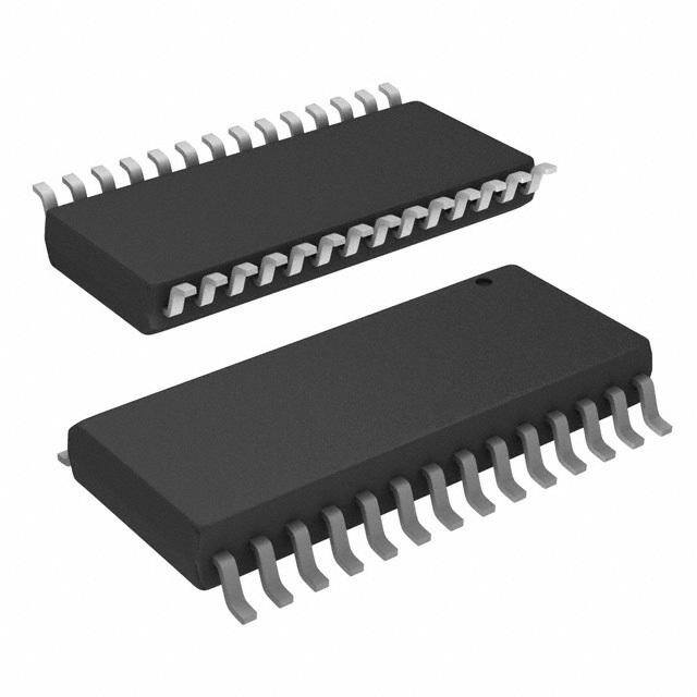
AD9708 ABSOLUTE MAXIMUM RATINGS* PIN FUNCTION DESCRIPTIONS With Pin No. Name Description Parameter Respect to Min Max Units 1 DB7 Most Significant Data Bit (MSB). AVDD ACOM –0.3 +6.5 V 2–7 DB6–DB1 Data Bits 1–6. DVDD DCOM –0.3 +6.5 V 8 DB0 Least Significant Data Bit (LSB). ACOM DCOM –0.3 +0.3 V 9–14,25 NC No Internal Connection. AVDD DVDD –6.5 +6.5 V 15 SLEEP Power-Down Control Input. Active CLOCK, SLEEP DCOM –0.3 DVDD + 0.3 V High. Contains active pull-down circuit, Digital Inputs DCOM –0.3 DVDD + 0.3 V thus may be left unterminated if not IOUTA, IOUTB ACOM –1.0 AVDD + 0.3 V used. COMP1, COMP2 ACOM –0.3 AVDD + 0.3 V 16 REFLO Reference Ground when Internal 1.2 V REFIO, FSADJ ACOM –0.3 AVDD + 0.3 V Reference Used. Connect to AVDD to REFLO ACOM –0.3 +0.3 V disable internal reference. Junction Temperature +150 (cid:176)C 17 REFIO Reference Input/Output. Serves as Storage Temperature –65 +150 (cid:176)C reference input when internal reference Lead Temperature disabled (i.e., Tie REFLO to AVDD). (10 sec) +300 (cid:176)C Serves as 1.2 V reference output when *Stresses above those listed under Absolute Maximum Ratings may cause perma- internal reference activated (i.e., Tie nent damage to the device. This is a stress rating only; functional operation of the REFLO to ACOM). Requires 0.1m F device at these or any other conditions above those indicated in the operational capacitor to ACOM when internal sections of this specification is not implied. Exposure to absolute maximum reference activated. ratings for extended periods may effect device reliability. 18 FS ADJ Full-Scale Current Output Adjust. THERMAL CHARACTERISTICS 19 COMP1 Bandwidth/Noise Reduction Node. Thermal Resistance Add 0.1 m F to AVDD for optimum 28-Lead 300 mil SOIC performance. q = 71.4(cid:176) C/W 20 ACOM Analog Common. JA q = 23(cid:176) C/W 21 IOUTB Complementary DAC Current Output. JC Full-scale current when all data bits 28-Lead TSSOP are 0s. q = 97.9(cid:176) C/W JA 22 IOUTA DAC Current Output. Full-scale q = 14.0(cid:176) C/W JC current when all data bits are 1s. 23 COMP2 Internal Bias Node for Switch Driver PIN CONFIGURATION Circuitry. Decouple to ACOM with 0.1m F capacitor. 24 AVDD Analog Supply Voltage (+2.7 V to (MSB) DB7 1 28 CLOCK +5.5 V). DB6 2 27 DVDD 26 DCOM Digital Common. DB5 3 26 DCOM 27 DVDD Digital Supply Voltage (+2.7 V to DB4 4 25 NC +5.5 V). DB3 5 24 AVDD AD9708 28 CLOCK Clock Input. Data latched on positive DB2 6 TOP VIEW 23 COMP2 DB1 7 (Not to Scale)22 IOUTA edge of clock. DB0 8 21 IOUTB NC 9 20 ACOM ORDERING GUIDE NC 10 19 COMP1 NC 11 18 FS ADJ Temperature Package Package NC 12 17 REFIO Model Range Descriptions Options* NC 13 16 REFLO AD9708AR –40(cid:176) C to +85(cid:176) C 28-Lead 300 Mil SOIC R-28 NC 14 15 SLEEP AD9708ARU –40(cid:176) C to +85(cid:176) C 28-Lead TSSOP RU-28 NC = NO CONNECT AD9708-EB Evaluation Board *R = Small Outline IC; RU = Thin Small Outline IC. CAUTION ESD (electrostatic discharge) sensitive device. Electrostatic charges as high as 4000 V readily WARNING! accumulate on the human body and test equipment and can discharge without detection. Although the AD9708 features proprietary ESD protection circuitry, permanent damage may occur on devices subjected to high energy electrostatic discharges. Therefore, proper ESD precautions are recommended to avoid performance degradation or loss of functionality. ESD SENSITIVE DEVICE –4– REV. B
AD9708 DEFINITIONS OF SPECIFICATIONS offset and gain drift, the drift is reported in ppm of full-scale Linearity Error (Also Called Integral Nonlinearity or INL) range (FSR) per degree C. For reference drift, the drift is Linearity error is defined as the maximum deviation of the reported in ppm per degree C. actual analog output from the ideal output, determined by a Power Supply Rejection straight line drawn from zero to full scale. The maximum change in the full-scale output as the supplies Differential Nonlinearity (or DNL) are varied from nominal to minimum and maximum specified DNL is the measure of the variation in analog value, normalized voltages. to full scale, associated with a 1 LSB change in digital input code. Settling Time Monotonicity The time required for the output to reach and remain within a A D/A converter is monotonic if the output either increases or specified error band about its final value, measured from the remains constant as the digital input increases. start of the output transition. Offset Error Glitch Impulse The deviation of the output current from the ideal of zero is Asymmetrical switching times in a DAC give rise to undesired called offset error. For IOUTA, 0 mA output is expected when output transients that are quantified by a glitch impulse. It is the inputs are all 0s. For IOUTB, 0 mA output is expected specified as the net area of the glitch in pV-s. when all inputs are set to 1s. Spurious-Free Dynamic Range Gain Error The difference, in dB, between the rms amplitude of the output The difference between the actual and ideal output span. The signal and the peak spurious signal over the specified bandwidth. actual span is determined by the output when all inputs are set Signal-to-Noise and Distortion (S/N+D, SINAD) Ratio to 1s minus the output when all inputs are set to 0s. S/N+D is the ratio of the rms value of the measured output Output Compliance Range signal to the rms sum of all other spectral components below the The range of allowable voltage at the output of a current-output Nyquist frequency, including harmonics but excluding dc. The DAC. Operation beyond the maximum compliance limits may value for S/N+D is expressed in decibels. cause either output stage saturation or breakdown resulting in Total Harmonic Distortion nonlinear performance. THD is the ratio of the rms sum of the first six harmonic Temperature Drift components to the rms value of the measured output signal. It is Temperature drift is specified as the maximum change from the expressed as a percentage or in decibels (dB). ambient (+25(cid:176) C) value to the value at either T or T . For MIN MAX +5V 0.1mF REFLO COMP1 AVDD ACOM 50pF +1.20V REF AD9708 0.1mF REF IO COMP2 CURRENT FS ADJ SAORURRACYE 0.1mF RSET 2kV +5V DVDD IOUTA SEGMENTED TO HP3589A DCOM SWITCHES IOUTB SPECTRUM/ NETWORK DVDD CLOSCLKEEP LATCHES 50V 20pF A50NVA LINYPZUETR DCOM 50V RETIMED 50V 20pF CLOCK DIGITAL OUTPUT* CLOCK DATA * AWG2021 CLOCK RETIMED OUTPUT LECROY 9210 TEKTRONIX SUCH THAT DIGITAL DATA PULSE GENERATOR AWG-2021 TRANSITIONS ON FALLING EDGE OF 50% DUTY CYCLE CLOCK. Figure 2.Basic AC Characterization Test Setup REV. B –5–
AD9708 Typical AC Characterization Curves (AVDD = +5 V or +3 V, DVDD = +5 V or +3 V, 50V Doubly Terminated Load, Single-Ended Output, I , I = 20 mA, T = +258C, unless otherwise noted) OUTA OUTFS A 70 70 55 THD @ 50MSPS THD @ 10MSPS 65 THD @ 10MSPS 65 IOUTFS = 20mA T@H 1D00MSPS T@H 1D00MSPS 50 IOUTFS = 10mA B 60 B 60 D – d D – d THD @ 50MSPS – dB 45 IOUTFS = 5mA SINAD/TH 5550 SINAD @ 10MSPS SINAD/TH 5505 SINAD @ 10MSPS SINAD 40 IOUTFS = 2.5mA SINAD @ 50MSPS SINAD @ 50MSPS 35 45 45 SINAD @ 100MSPS SINAD @ 100MSPS 40 40 30 0.1 1 10 100 0.1 1 10 100 1 10 100 FREQUENCY – MHz FREQUENCY – MHz FREQUENCY – MHz Figure 3.SINAD/THD vs. f (AVDD Figure 4.SINAD/THD vs. f (Differ- Figure 5.SINAD vs. I OUT OUT OUTFS and DVDD = 5.0 V) ential Output, AVDD and DVDD = 5.0 V) @ 100 MSPS 70 70 52 65 THD @ 10MSPS THD 65 @ 1T0HMDSPS T@H 5D0MSPS 50 IOUTFS = 10mA IOUTFS = 20mA @ 100MSPS B 60 B 60 IOUTFS = 5mA d d SINAD/THD – 5505 SINAD @ 10TMHSDP S@ 50MSPS SINAD/THD – 5505 SINAD @ 10MSTPHSD @ 100MSPS SINAD – dB 4468 IOUTFS = 2.5mA SINAD @ 50MSPS SINAD @ 50MSPS 44 45 45 SINAD @ 100MSPS SINAD @ 100MSPS 40 40 42 0.1 1 10 100 0.1 1 10 100 0.1 1 10 FREQUENCY – MHz FREQUENCY – MHz FREQUENCY – MHz Figure 6.SINAD/THD vs. f (AVDD Figure 7.SINAD/THD vs. f (Differ- Figure 8.SINAD vs. I OUT OUT OUTFS and DVDD = 3.0 V) ential Output, AVDD and DVDD = 3.0 V) @ 20 MSPS 0 0 0.6 fCLOCK = 25MSPS fCLOCK = 125MSPS fOUT = 7.81MHz fOUT = 27.0MHz 0.5 SFDR = +60.7dBc SFDR = +52.7dBc AMPLITUDE = 0dBFS AMPLITUDE = 0dBc 0.4 10dB – Div 10dB – Div VOLTS000...321 0.0 –0.1 –100 –100 –0.2 START: 0Hz STOP: 12.5MHz START: 0Hz STOP: 62.5MHz TIME – 5ns/Div Figure 9.Single-Tone Spectral Plot Figure 10.Single-Tone Spectral Figure 11.Step Response @ 25 MSPS Plot @ 125 MSPS –6– REV. B
AD9708 FUNCTIONAL DESCRIPTION As previously mentioned, I is a function of the reference OUTFS Figure 12 shows a simplified block diagram of the AD9708. The current I , which is nominally set by a reference voltage REF AD9708 consists of a large PMOS current source array capable of V and external resistor R . It can be expressed as: REFIO SET providing up to 20mA of total current. The array is divided into I = 32 · I (3) 31 equal currents that make up the five most significant bits OUTFS REF (MSBs). The remaining 3 LSBs are also implemented with equally where weighted current sources whose sum total equals 7/8th of an IREF = VREFIO/RSET (4) MSB current source. Implementing the upper and lower bits The two current outputs will typically drive a resistive load with current sources helps maintain the DAC’s high output directly. If dc coupling is required, IOUTA and IOUTB should impedance (i.e. > 100 kW ). All of these current sources are be directly connected to matching resistive loads, R , which LOAD switched to one or the other of the two output nodes (i.e., IOUTA are tied to analog common, ACOM. Note, R may repre- LOAD or IOUTB) via PMOS differential current switches. The switches sent the equivalent load resistance seen by IOUTA or IOUTB are based on a new architecture that drastically improves as would be the case in a doubly terminated 50W or 75W cable. distortion performance. The single-ended voltage output appearing at the IOUTA and The analog and digital sections of the AD9708 have separate IOUTB nodes is simply: power supply inputs (i.e., AVDD and DVDD) that can operate V = I · R (5) OUTA OUTA LOAD independently over a 2.7 volt to 5.5 volt range. The digital section, V = I · R (6) which is capable of operating up to a 125 MSPS clock rate, OUTB OUTB LOAD consists of edge-triggered latches and segment decoding logic Note the full-scale value of VOUTA and VOUTB should not exceed circuitry. The analog section includes the PMOS current the specified output compliance range to maintain specified sources, the associated differential switches, a 1.20 V bandgap distortion and linearity performance. voltage reference and a reference control amplifier. The differential voltage, V , appearing across IOUTA and DIFF The full-scale output current is regulated by the reference con- IOUTB is: trol amplifier and can be set from 2 mA to 20 mA via an exter- V = (I – I ) · R (7) DIFF OUTA OUTB LOAD nal resistor, R . The external resistor, in combination with SET Substituting the values of I , I , and I ; V can be both the reference control amplifier and voltage reference OUTA OUTB REF DIFF expressed as: V , sets the reference current I , which is mirrored over to REFIO REF the segmented current sources with the proper scaling factor. V = {(2 DAC CODE – 255)/256}/ · (32 R /R ) DIFF LOAD SET The full-scale current, I , is thirty-two times the value of I . · V (8) OUTFS REF REFIO DAC TRANSFER FUNCTION VOLTAGE REFERENCE AND CONTROL AMPLIFIER The AD9708 provides complementary current outputs, IOUTA The AD9708 contains an internal 1.20 V bandgap reference and IOUTB. IOUTA will provide a near full-scale current output, that can be easily disabled and overridden by an external refer- I , when all bits are high (i.e., DAC CODE = 255), while ence. REFIO serves as either an input or output depending on OUTFS IOUTB, the complementary output, provides no current. The whether the internal or an external reference is selected. If current output appearing at IOUTA and IOUTB are a function REFLO is tied to ACOM, as shown in Figure 13, the internal of both the input code and I and can be expressed as: reference is activated and REFIO provides a 1.20V output. In OUTFS I = (DAC CODE/256) · I (1) this case, the internal reference must be compensated externally OUTA OUTFS with a ceramic chip capacitor of 0.1m F or greater from REFIO IOUTB = (255 – DAC CODE)/256 · IOUTFS (2) to REFLO. Note that REFIO is not designed to drive any ex- where DAC CODE = 0 to 255 (i.e., Decimal Representation). ternal load. It should be buffered with an external amplifier having an input bias current less than 100nA if any additional loading is required. +5V 0.1mF REFLO COMP1 AVDD ACOM +1.20V REF 50pF AD9708 VREFIO REFIO COMP2 0.1mF CURRENT 0.1mF IREF FS ADJ SAORURRACYE R2SkEVT VDIFF = VOUTA – VOUTB +5V DVDD IOUTA IOUTA DCOM SSEWGMITECNHTEESD IOUTB IOUTB VOUTB RVLOOUATDA CLOCK CLOCK LATCHES RLOAD 50V SLEEP 50V DIGITAL DATA INPUTS (DB7–DB0) Figure 12.Functional Block Diagram REV. B –7–
AD9708 +5V The small signal bandwidth of the reference control amplifier is 0.1mF approximately 1.8 MHz and can be reduced by connecting an OPTIONAL EXTERNAL external capacitor between COMP1 and AVDD. The output of REF BUFFER REFLO COMP1 AVDD the control amplifier, COMP1, is internally compensated via a +1.2V REF 50 pF capacitor that limits the control amplifier small-signal 50pF bandwidth and reduces its output impedance. Any additional REFIO ADDITIONAL CURRENT external capacitance further limits the bandwidth and acts as LOAD 0.1mF FS ADJ SAORURRACYE a filter to reduce the noise contribution from the reference 2kV AD9708 amplifier. If I is fixed for an application, a 0.1m F ceramic chip REF capacitor is recommended. Figure 13.Internal Reference Configuration I can be varied for a fixed R by disabling the internal REF SET The internal reference can be disabled by connecting REFLO to reference and varying the common-mode voltage over its AVDD. In this case, an external reference may then be applied compliance range of 1.25 V to 0.10 V. REFIO can be driven by to REFIO as shown in Figure 14. The external reference may a single-supply amplifier or DAC, thus allowing IREF to be var- provide either a fixed reference voltage to enhance accuracy and ied for a fixed RSET. Since the input impedance of REFIO is drift performance or a varying reference voltage for gain control. approximately 1 MW , a simple R-2R ladder DAC configured in Note that the 0.1m F compensation capacitor is not required the voltage mode topology may be used to control the gain. This since the internal reference is disabled, and the high input circuit is shown in Figure 15 using the AD7524 and an external impedance (i.e., 1 MW ) of REFIO minimizes any loading of the 1.2 V reference, the AD1580. Note another AD9708 could also external reference. be used as the gain control DAC since it can also provide a programmable unipolar output up to 1.2 V. AVDD ANALOG OUTPUTS AND OUTPUT CONFIGURATIONS 0.1mF The AD9708 produces two complementary current outputs, I and I , which may be converted into complementary OUTA OUTB single-ended voltage outputs, V and V , via a load resistor, AVDD REFLO COMP1 AVDD OUTA OUTB R , as described in the DAC TRANSFER FUNCTION +1.2V REF LOAD 50pF section. Figure 16 shows the AD9708 configured to provide a EXTERNAL VREFIO REFIO CURRENT positive unipolar output range of approximately 0 V to +0.5 V REF FS ADJ SAORURRACYE for a double terminated 50 W cable for a nominal full-scale RSET IREF = current, IOUTFS, of 20 mA. In this case, RLOAD represents the VREFIO/RSET AD9708 RCEOFNETRREONLCE equivalent load resistance seen by IOUTA or IOUTB and is AMPLIFIER equal to 25 W . The unused output (IOUTA or IOUTB) can be connected to ACOM directly or via a matching R . Different LOAD Figure 14.External Reference Configuration values of I and R can be selected as long as the posi- OUTFS LOAD tive compliance range is adhered to. The AD9708 also contains an internal control amplifier that is used to regulate the DAC’s full-scale output current, I . OUTFS The control amplifier is configured as a V-I converter, as shown AD9708 in Figure 14, such that its current output, I , is determined by IOUTFS = 20mA VOUTA = 0 TO +0.5V REF IOUTA 22 the ratio of the V and an external resistor, R , as stated REFIO SET 50V 50V in Equation 4. The control amplifier allows a wide (10:1) IOUTB 21 adjustment span of I over a 2mA to 20 mA range by setting OUTFS 25V I between 62.5m A and 625m A. The wide adjustment span of REF I provides several application benefits. The first benefit OUTFS relates directly to the power dissipation of the AD9708, which is Figure 16.0 V to +0.5V Unbuffered Voltage Output proportional to IOUTFS (refer to the POWER DISSIPATION Alternatively, an amplifier could be configured as an I-V converter section). The second benefit relates to the 20dB adjustment, thus converting IOUTA or IOUTB into a negative unipolar which is useful for system gain control purposes. AVDD AVDD OPTIONAL BANDLIMITING CAPACITOR REFLO COMP1 AVDD RFB VDD +1.2V REF 50pF 1.2V OUT1 0.1V TO 1.2V REFIO AD7524 VREF CURRENT AD1580 OUT2 FS ADJ SOURCE ARRAY AGND RSET IREF = AD9708 VREF/RSET DB7–DB0 Figure 15.Single-Supply Gain Control Circuit –8– REV. B
AD9708 voltage. Figure 17 shows a buffered singled-ended output con- over a digital supply range of 2.7 V to 5.5 V. As a result, the figuration in which the op amp, U1, performs an I-V conversion digital inputs can also accommodate TTL levels when DVDD is on the AD9708 output current. U1 provides a negative unipolar set to accommodate the maximum high level voltage, V , OH(MAX) output voltage and its full-scale output voltage is simply the of the TTL drivers. A DVDD of 3 V to 3.3 V will typically product of R and I . The full-scale output should be set ensure upper compatibility of most TTL logic families. FB OUTFS within U1’s voltage output swing capabilities by scaling I OUTFS and/or RFB. An improvement in ac distortion performance may DVDD result with a reduced I , since the signal current U1 will be OUTFS required to sink and will be subsequently reduced. Note, the ac distortion performance of this circuit at higher DAC update DIGITAL rates may be limited by U1’s slewing capabilities. INPUT COPT RFB Figure 18.Equivalent Digital Input 200V AD9708 IOUTFS = 10mA Since the AD9708 is capable of being updated up to 125 MSPS, IOUTA 22 the quality of the clock and data input signals are important in U1 VOUT = IOUTFS 3 RFB achieving the optimum performance. The drivers of the digital IOUTB 21 data interface circuitry should be specified to meet the minimum 200V setup-and-hold times of the AD9708 as well as its required min/ max input logic level thresholds. Typically, the selection of the slowest logic family that satisfies the above conditions will result Figure 17.Unipolar Buffered Voltage Output in the lowest data feedthrough and noise. IOUTA and IOUTB also have a negative and positive voltage Digital signal paths should be kept short and run lengths matched compliance range that must be adhered to in order to achieve to avoid propagation delay mismatch. The insertion of a low optimum performance. The positive output compliance range is value resistor network (i.e., 20W to 100W ) between the AD9708 slightly dependent on the full-scale output current, I . It OUTFS digital inputs and driver outputs may be helpful in reducing any degrades slightly from its nominal 1.25 V for an I = 20 mA OUTFS overshooting and ringing at the digital inputs that contribute to to 1.00 V for an I = 2 mA. Applications requiring the OUTFS data feedthrough. For longer run lengths and high data update AD9708’s output (i.e., V and/or V ) to extend up to its OUTA OUTB rates, strip line techniques with proper termination resistors output compliance range should size R accordingly. Operation LOAD should be considered to maintain “clean” digital inputs. Also, beyond this compliance range will adversely affect the AD9708’s operating the AD9708 with reduced logic swings and a corre- linearity. sponding digital supply (DVDD) will also reduce data feedthrough. The differential voltage, V , existing between V and DIFF OUTA The external clock driver circuitry should provide the AD9708 V may also be converted to a single-ended voltage via a OUTB with a low jitter clock input meeting the min/max logic levels transformer or differential amplifier configuration. Refer to the while providing fast edges. Fast clock edges will help minimize DIFFERENTIAL OUTPUT CONFIGURATION section for any jitter that will manifest itself as phase noise on a recon- more information. structed waveform. However, the clock input could also be DIGITAL INPUTS driven by via a sine wave, which is centered around the digital The AD9708’s digital input consists of eight data input pins and threshold (i.e., DVDD/2), and meets the min/max logic threshold. a clock input pin. The 8-bit parallel data inputs follow standard This may result in a slight degradation in the phase noise, which positive binary coding where DB7 is the most significant bit becomes more noticeable at higher sampling rates and output (MSB) and DB0 is the least significant bit (LSB). The digital frequencies. Note, at higher sampling rates the 20% tolerance interface is implemented using an edge-triggered master slave of the digital logic threshold should be considered since it will latch. The DAC output is updated following the rising edge of affect the effective clock duty cycle and subsequently cut into the clock as shown in Figure 1 and is designed to support a the required data setup-and-hold times. clock rate as high as 125 MSPS. The clock can be operated at any duty cycle that meets the specified latch pulsewidth. The SLEEP MODE OPERATION setup-and-hold times can also be varied within the clock cycle as The AD9708 has a power-down function that turns off the long as the specified minimum times are met; although the output current and reduces the supply current to less than 8.5mA location of these transition edges may affect digital feedthrough over the specified supply range of 2.7V to 5.5 V and tempera- and distortion performance. ture range. This mode can be activated by applying a logic level “1” to the SLEEP pin. This digital input also contains an active The digital inputs are CMOS compatible with logic thresholds, pull-down circuit that ensures the AD9708 remains enabled if V set to approximately half the digital positive supply THRESHOLD this input is left disconnected. The SLEEP input with active (DVDD) or pull-down requires <40m A of drive current. V = DVDD/2 (– 20%) THRESHOLD The power-up and power-down characteristics of the AD9708 Figure 18 shows the equivalent digital input circuit for the data are dependent on the value of the compensation capacitor con- and clock inputs. The sleep mode input is similar, except that nected to COMP2 (Pin 23). With a nominal value of 0.1m F, the it contains an active pull-down circuit, thus ensuring that the AD9708 takes less than 5m s to power down and approximately AD9708 remains enabled if this input is left disconnected. The 3.25ms to power back up. internal digital circuitry of the AD9708 is capable of operating REV. B –9–
AD9708 30 18 8 125MSPS 125MSPS 16 25 14 100MSPS 6 100MSPS 20 12 A A A m m10 m – D15 – D – D4 D D 8 D AV DV 50MSPS DV 50MSPS I10 I 6 I 4 25MSPS 2 25MSPS 5 2 5MSPS 5MSPS 0 0 0 2 4 6 8 10 12 14 16 18 20 0.01 0.1 1 0.01 0.1 1 IOUTFS – mA RATIO (fOUT/fCLK) RATIO (fOUT/fCLK) Figure 19.IAVDD vs. IOUTFS Figure 20.IDVDD vs. Ratio Figure 21.IDVDD vs. Ratio @ DVDD = 5 V @ DVDD = 3 V POWER DISSIPATION FERRITE The power dissipation, P , of the AD9708 is dependent on BEADS D several factors, including: (1) AVDD and DVDD, the power TTL/CMOS AVDD LOGIC 100mF 10-22mF 0.1mF supply voltages; (2) I , the full-scale current output; (3) CIRCUITS ELECT. TANT. CER. OUTFS f , the update rate; (4) and the reconstructed digital input ACOM CLOCK waveform. The power dissipation is directly proportional to the analog supply current, I , and the digital supply current, AVDD IDVDD. IAVDD is directly proportional to IOUTFS, as shown in +5V OR +3V Figure 19, and is insensitive to f . POWER SUPPLY CLOCK Conversely, I is dependent on both the digital input wave- Figure 22.Differential LC Filter for Single +5V or +3 V DVDD form, f , and digital supply DVDD. Figures 20 and 21 Applications CLOCK show I as a function of full-scale sine wave output ratios DVDD Maintaining low noise on power supplies and ground is critical (f /f ) for various update rates with DVDD = 5 V and OUT CLOCK to obtaining optimum results from the AD9708. If properly DVDD = 3 V, respectively. Note, how I is reduced by more DVDD implemented, ground planes can perform a host of functions on than a factor of 2 when DVDD is reduced from 5 V to 3V. high speed circuit boards: bypassing, shielding, current trans- port, etc. In mixed signal design, the analog and digital portions APPLYING THE AD9708 of the board should be distinct from each other, with the analog Power and Grounding Considerations ground plane confined to the areas covering the analog signal In systems seeking to simultaneously achieve high speed and traces, and the digital ground plane confined to areas covering high performance, the implementation and construction of the the digital interconnects. printed circuit board design is often as important as the circuit design. Proper RF techniques must be used in device selection All analog ground pins of the DAC, reference and other analog placement and routing and supply bypassing and grounding. components, should be tied directly to the analog ground plane. The evaluation board for the AD9708, which uses a four layer The two ground planes should be connected by a path 1/8 to PC board, serves as a good example for the above mentioned 1/4 inch wide underneath or within 1/2 inch of the DAC to considerations. The evaluation board provides an illustration of maintain optimum performance. Care should be taken to ensure the recommended printed circuit board ground, power and that the ground plane is uninterrupted over crucial signal paths. signal plane layouts. On the digital side, this includes the digital input lines running to the DAC as well as any clock signals. On the analog side, this Proper grounding and decoupling should be a primary objective includes the DAC output signal, reference signal and the supply in any high speed system. The AD9708 features separate analog feeders. and digital supply and ground pins to optimize the management of analog and digital ground currents in a system. In general, The use of wide runs or planes in the routing of power lines is AVDD, the analog supply, should be decoupled to ACOM, the also recommended. This serves the dual role of providing a low analog common, as close to the chip as physically possible. Simi- series impedance power supply to the part, as well as providing larly, DVDD, the digital supply, should be decoupled to DCOM some “free” capacitive decoupling to the appropriate ground as close as physically as possible. plane. It is essential that care be taken in the layout of signal and power ground interconnects to avoid inducing extraneous For those applications requiring a single +5V or +3 V supply voltage drops in the signal ground paths. It is recommended that for both the analog and digital supply, a clean analog supply all connections be short, direct and as physically close to the may be generated using the circuit shown in Figure 22. The package as possible in order to minimize the sharing of conduc- circuit consists of a differential LC filter with separate power tion paths between different currents. When runs exceed an inch supply and return lines. Lower noise can be attained using low in length, strip line techniques with proper termination resistor ESR type electrolytic and tantalum capacitors. –10– REV. B
AD9708 should be considered. The necessity and value of this resistor 500V will be dependent upon the logic family used. AD9708 225V For a more detailed discussion of the implementation and IOUTA 22 construction of high speed, mixed signal printed circuit boards, 225V AD8072 refer to Analog Devices’ application notes AN-280 and AN-333. IOUTB 21 COPT 500V DIFFERENTIAL OUTPUT CONFIGURATIONS 25V 25V For applications requiring the optimum dynamic performance and/or a bipolar output swing, a differential output configura- Figure 24.DC Differential Coupling Using an Op Amp tion is suggested. A differential output configuration may con- sists of either an RF transformer or a differential op amp The common-mode rejection of this configuration is typically configuration. The transformer configuration is well suited for determined by the resistor matching. In this circuit, the differ- ac coupling applications. It provides the optimum high fre- ential op amp circuit is configured to provide some additional quency performance due to its excellent rejection of common- signal gain. The op amp must operate off a dual supply since its mode distortion (i.e., even-order harmonics) and noise over a output is approximately – 1.0V. A high speed amplifier capable wide frequency range. It also provides electrical isolation and of preserving the differential performance of the AD9708 while the ability to deliver twice the power to the load (i.e., assuming meeting other system level objectives (i.e., cost, power) should no source termination). The differential op amp configuration is be selected. The op amps differential gain, its gain setting resis- suitable for applications requiring dc coupling, a bipolar output, tor values and full-scale output swing capabilities should all be signal gain, and/or level shifting. considered when optimizing this circuit. Figure 23 shows the AD9708 in a typical transformer coupled The differential circuit shown in Figure 25 provides the neces- output configuration. The center-tap on the primary side of the sary level-shifting required in a single supply system. In this transformer must be connected to ACOM to provide the necessary case, AVDD, which is the positive analog supply for both the dc current path for both IOUTA and IOUTB. The complemen- AD9708 and the op amp, is also used to level-shift the differ- tary voltages appearing at IOUTA and IOUTB (i.e., V and ential output of the AD9762 to midsupply (i.e., AVDD/2). OUTA V ) swing symmetrically around ACOM and should be OUTB maintained within the specified output compliance range of the 500V AD9708. A differential resistor, RDIFF, may be inserted in AD9708 225V applications in which the output of the transformer is connected IOUTA 22 to the load, RLOAD, via a passive reconstruction filter or cable. 225V AD8072 RDIFF is determined by the transformer’s impedance ratio and IOUTB 21 provides the proper source termination. Note that approxi- COPT 1kV AVDD mately half the signal power will be dissipated across R . DIFF 25V 25V 1kV MINI-CIRCUITS T1-1T IOUTA 22 Figure 25.Single-Supply DC Differential Coupled Circuit AD9708 RLOAD AD9708 EVALUATION BOARD IOUTB 21 General Description OPTIONAL RDIFF The AD9708-EB is an evaluation board for the AD9708 8-bit D/A converter. Careful attention to layout and circuit design, Figure 23.Differential Output Using a Transformer combined with a prototyping area, allows the user to easily and An op amp can also be used to perform a differential to single- effectively evaluate the AD9708 in any application where high ended conversion as shown in Figure 24. The AD9708 is resolution, high speed conversion is required. configured with two equal load resistors, RLOAD, of 25 W . The This board allows the user the flexibility to operate the AD9708 differential voltage developed across IOUTA and IOUTB is in various configurations. Possible output configurations include converted to a single-ended signal via the differential op amp transformer coupled, resistor terminated, inverting/noninverting configuration. An optional capacitor can be installed across and differential amplifier outputs. The digital inputs are IOUTA and IOUTB forming a real pole in a low-pass filter. designed to be driven directly from various word generators, The addition of this capacitor also enhances the op amps distortion with the on-board option to add a resistor network for proper performance by preventing the DACs high slewing output from load termination. Provisions are also made to operate the overloading the op amp’s input. AD9708 with either the internal or external reference, or to exercise the power-down feature. Refer to the application note AN-420 “Using the AD9760/ AD9762/AD9764-EB Evaluation Board” for a thorough description and operating instructions for the AD9708 evalua- tion board. REV. B –11–
AD9708 P13 T B A 3 2 1 JP3 VEE TP8C9m0.1F A OUT 1OUT 2 TP9 C10m0.1F AVDD AVCC C17m0.1F U6A376AD804724AJP5 123A C15m0.1FR46VA1k AVDDC8m0.1F TP10 R16V2kC11TP14m0.1F JP4 AA R42V1k6 R43V5kCW A C14R45m1FV1k C7m1F AVDD TP11 AVDD 1 2 3JP2NA U7 REF432VINVOUT GND 4A XTREFINJ5 R44V50AA B 3 A PDIJ2 C C16m1F E CLKTP1JP1A 21R15V49.9 U1 AD970828B13CLOCK27B12DVDD26B11DCOM25B10NC24B9AVDD23B8COMP222IB7OUTA21IB6OUTB20B5ACOM19COMP1B418B3FS ADJ17B2REFIO16B1REFLO15B0SLEEP CT1 A TP12 R17V49.9 AVC C18m0.1F A DDDDDDDDDDDDDD J1 101234567891011121314 1 DVDD J6 A EXTCLK 9876 432 C22m1F R37V49.9 C24m1F C B6 TP7 C6Am10F DVDD R7 1 10543298 21098765 1 R8 AVCC C21m0.1FU437A6AD804724 R36V1k C23m0.1F AAVEE C 7 3 AV 654 654 R18V1k JP8 B A R35V1k B5 TP6 C5Am10F R3 1 32 10987 R4 A P7A B R10V1kA A B A AVEE B4 TP19TP18 TP5 16 PINDIPRES PK 11621514341312511671098 16 PINDIPRES PK 161152143134125116107 JP7BJ B A R9V1k JP9 AGNDAVDD B3B2 TP4TP2 C4Am10F DVDD R5 1 101098765432C19C1C2C25C26C27C28C29 C30C31C32C33C34C35C36 1098765432 11 R6DVDD JP6A J7R12OPENT1C2030A JP6B1 R13OPENA A GND 98 2 4 5 A 6 D 7 3 DVDD B1 TP3 C3m10F R1 1P16543213579111315171921232527293133353739 98765410 R2 J3OUT1 C12R20V22pF49.9 AAR140 J4OUT2 C13R38V22pF49.9 AA 246810121416182022242628303234363840 Figure 26.Evaluation Board Schematic –12– REV. B
AD9708 Figure 27.Silkscreen Layer—Top Figure 28.Component Side PCB Layout (Layer 1) REV. B –13–
AD9708 Figure 29.Ground Plane PCB Layout (Layer 2) Figure 30.Power Plane PCB Layout (Layer 3) –14– REV. B
AD9708 Figure 31.Solder Side PCB Layout (Layer 4) Figure 32.Silkscreen Layer—Bottom REV. B –15–
AD9708 OUTLINE DIMENSIONS Dimensions shown in inches and (mm). 28-Lead, 300 Mil SOIC (R-28) 0.7125 (18.10) 99 0.6969 (17.70) 4/ – 1 – b 28 15 79 0.2992 (7.60) 9 2 0.2914 (7.40) C 0.4193 (10.65) 1 14 0.3937 (10.00) PIN 1 0.1043 (2.65) 0.0291 (0.74) 0.0926 (2.35) 0.0098 (0.25)3 458 88 00..00101480 ((00..3100)) 0(B.10.S52C070) 00..00119328 ((00..4395)) SPELAANTIENG 00..00102951 ((00..3223)) 08 00..00510507 ((10..2470)) 28-Lead TSSOP (RU-28) 0.386 (9.80) 0.378 (9.60) 28 15 0.177 (4.50)0.169 (4.30) 0.256 (6.50)0.246 (6.25) 1 14 PIN 1 0.006 (0.15) 0.002 (0.05) 0.0433 (1.10) MAX 8° 0.028 (0.70) SEPALTAINNGE 0.02B56S C(0.65) 00..00101785 ((00..3109)) 00.0.0003759 ( (00.0.2900))0° 0.020 (0.50) A. S. U. N D I E T N RI P –16– REV. B