ICGOO在线商城 > 集成电路(IC) > 数据采集 - 模数转换器 > AD9211BCPZ-250
 Datasheet下载
- 型号: AD9211BCPZ-250
- 制造商: Analog
- 库位|库存: xxxx|xxxx
- 要求:
| 数量阶梯 | 香港交货 | 国内含税 |
| +xxxx | $xxxx | ¥xxxx |
查看当月历史价格
查看今年历史价格
AD9211BCPZ-250产品简介:
ICGOO电子元器件商城为您提供AD9211BCPZ-250由Analog设计生产,在icgoo商城现货销售,并且可以通过原厂、代理商等渠道进行代购。 AD9211BCPZ-250价格参考。AnalogAD9211BCPZ-250封装/规格:数据采集 - 模数转换器, 10 Bit Analog to Digital Converter 1 Input 1 Pipelined 56-LFCSP-VQ (8x8)。您可以下载AD9211BCPZ-250参考资料、Datasheet数据手册功能说明书,资料中有AD9211BCPZ-250 详细功能的应用电路图电压和使用方法及教程。
AD9211BCPZ-250 是 Analog Devices Inc.(ADI)推出的一款高速模数转换器(ADC),广泛应用于需要高精度和高速信号处理的场景。其主要应用场景包括:

1. 通信系统:用于无线基站、软件定义无线电(SDR)等设备中,将接收到的模拟射频信号转换为数字信号,便于后续数字信号处理。

2. 测试与测量设备:如示波器、频谱分析仪等,用于高精度采集和分析高频信号。

3. 工业控制与自动化:在高精度传感器信号采集系统中,实现对模拟量的快速数字化处理,提升系统响应速度和精度。

4. 医疗成像设备:如超声波设备、CT扫描仪等,用于采集和处理来自探测器的模拟信号,提升图像质量和诊断准确性。

5. 雷达与国防电子:用于雷达接收机和电子战系统中,实现对高频信号的实时采集和处理,提高系统的探测和反应能力。

该ADC具有12位分辨率、最高采样率可达250MSPS,采用1.8V电源供电,具备低功耗、高性能的特点,适合对速度和精度都有较高要求的应用场景。
| 参数 | 数值 |
| 产品目录 | 集成电路 (IC)半导体 |
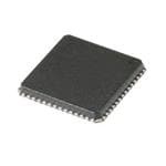
| 描述 | IC ADC 10-BIT 250MSPS 56-LFCSP模数转换器 - ADC 10-Bit 250 Msps 1.8V |
| 产品分类 | |
| 品牌 | Analog Devices |
| 产品手册 | |
| 产品图片 |
|
| rohs | 符合RoHS无铅 / 符合限制有害物质指令(RoHS)规范要求 |
| 产品系列 | 数据转换器IC,模数转换器 - ADC,Analog Devices AD9211BCPZ-250- |
| 数据手册 | |
| 产品型号 | AD9211BCPZ-250 |
| 产品种类 | 模数转换器 - ADC |
| 位数 | 10 |
| 供应商器件封装 | 56-LFCSP-VQ(8x8) |
| 信噪比 | 59.5 dB |
| 其它名称 | AD9211BCPZ250 |
| 分辨率 | 10 bit |
| 包装 | 托盘 |
| 商标 | Analog Devices |
| 安装类型 | 表面贴装 |
| 安装风格 | SMD/SMT |
| 封装 | Tray |
| 封装/外壳 | 56-VFQFN 裸露焊盘,CSP |
| 封装/箱体 | LFCSP-56 |
| 工作温度 | -40°C ~ 85°C |
| 工作电源电压 | 1.8 V |
| 工厂包装数量 | 260 |
| 接口类型 | Parallel |
| 数据接口 | SPI |
| 最大功率耗散 | 437 mW |
| 最大工作温度 | + 85 C |
| 最小工作温度 | - 40 C |
| 标准包装 | 1 |
| 特性 | - |
| 电压参考 | Internal |
| 电压源 | 模拟和数字 |
| 系列 | AD9211 |
| 结构 | Pipeline |
| 转换器数 | 1 |
| 转换器数量 | 1 |
| 转换速率 | 300 MS/s |
| 输入数和类型 | 2 个单端,单极1 个差分,单极 |
| 输入类型 | Differential |
| 通道数量 | 1 Channel |
| 配用 | /product-detail/zh/AD9211-300EBZ/AD9211-300EBZ-ND/1551778/product-detail/zh/AD9211-250EBZ/AD9211-250EBZ-ND/1551333/product-detail/zh/AD9211-200EBZ/AD9211-200EBZ-ND/1551332 |
| 采样率(每秒) | 250M |


- 商务部:美国ITC正式对集成电路等产品启动337调查
- 曝三星4nm工艺存在良率问题 高通将骁龙8 Gen1或转产台积电
- 太阳诱电将投资9.5亿元在常州建新厂生产MLCC 预计2023年完工
- 英特尔发布欧洲新工厂建设计划 深化IDM 2.0 战略
- 台积电先进制程称霸业界 有大客户加持明年业绩稳了
- 达到5530亿美元!SIA预计今年全球半导体销售额将创下新高
- 英特尔拟将自动驾驶子公司Mobileye上市 估值或超500亿美元
- 三星加码芯片和SET,合并消费电子和移动部门,撤换高东真等 CEO
- 三星电子宣布重大人事变动 还合并消费电子和移动部门
- 海关总署:前11个月进口集成电路产品价值2.52万亿元 增长14.8%


PDF Datasheet 数据手册内容提取
10-Bit, 200 MSPS/250 MSPS/300 MSPS, 1.8 V Analog-to-Digital Converter AD9211 FEATURES FUNCTIONAL BLOCK DIAGRAM SNR = 60.1 dBFS @ f up to 70 MHz @ 300 MSPS RBIAS PWDN AGND AVDD (1.8V) IN ENOB of 9.7 @ f up to 70 MHz @ 300 MSPS (−1.0 dBFS) IN SFDR = −80 dBc @ f up to 70 MHz @ 300 MSPS (−1.0 dBFS) REFERENCE AD9211 IN Excellent linearity DRVDD DNL = ±0.1 LSB typical VIN+ DGND TRACK-AND-HOLD INL = ±0.2 LSB typical VIN– ADC 10 OUTPUT 10 LVDS at 300 MSPS (ANSI-644 levels) 10-BIT STAGING D9 TO D0 CORE LVDS 700 MHz full power analog bandwidth CLK+ CLOCK OR+ On-chip reference, no external decoupling required CLK– MANAGEMENT OR– Integrated input buffer and track-and-hold SERIAL PORT Low power dissipation DCO+ 443170 mmWW @@ 330000 MMSSPPSS——LLVVDDSS SDDDRR mmooddee RESETSCLK SDIO CSB DCO– 06041-001 Programmable input voltage range Figure 1. 1.0 V to 1.5 V, 1.25 V nominal 1.8 V analog and digital supply operation Selectable output data format (offset binary, twos complement, Gray code) Clock duty cycle stabilizer Integrated data capture clock APPLICATIONS Wireless and wired broadband communications Cable reverse path Communications test equipment Radar and satellite subsystems Power amplifier linearization GENERAL DESCRIPTION PRODUCT HIGHLIGHTS The AD9211 is a 10-bit monolithic sampling analog-to-digital 1. High Performance—Maintains 60.1 dBFS SNR @ converter optimized for high performance, low power, and ease 300 MSPS with a 70 MHz input. of use. The product operates at up to a 300 MSPS conversion 2. Low Power—Consumes only 410 mW @ 300 MSPS. rate and is optimized for outstanding dynamic performance 3. Ease of Use—LVDS output data and output clock signal in wideband carrier and broadband systems. All necessary allow interface to current FPGA technology. The on-chip functions, including a track-and-hold (T/H) and voltage reference and sample-and-hold provide flexibility in reference, are included on the chip to provide a complete system design. Use of a single 1.8 V supply simplifies signal conversion solution. system power supply design. 4. Serial Port Control—Standard serial port interface The ADC requires a 1.8 V analog voltage supply and a supports various product functions, such as data differential clock for full performance operation. The digital formatting, disabling the clock duty cycle stabilizer, power- outputs are LVDS (ANSI-644) compatible and support either down, gain adjust, and output test pattern generation. twos complement, offset binary format, or Gray code. A data 5. Pin-Compatible Family—12-bit pin-compatible family clock output is available for proper output data timing. offered as AD9230. Fabricated on an advanced CMOS process, the AD9211 is available in a 56-lead LFCSP, specified over the industrial temperature range (−40°C to +85°C). Rev. 0 Information furnished by Analog Devices is believed to be accurate and reliable. However, no responsibility is assumed by Analog Devices for its use, nor for any infringements of patents or other One Technology Way, P.O. Box 9106, Norwood, MA 02062-9106, U.S.A. rights of third parties that may result from its use. Specifications subject to change without notice. No license is granted by implication or otherwise under any patent or patent rights of Analog Devices. Tel: 781.329.4700 www.analog.com Trademarks and registered trademarks are the property of their respective owners. Fax: 781.461.3113 ©2007 Analog Devices, Inc. All rights reserved.
AD9211 TABLE OF CONTENTS Features..............................................................................................1 Theory of Operation......................................................................19 Applications.......................................................................................1 Analog Input and Voltage Reference.......................................19 Functional Block Diagram..............................................................1 Clock Input Considerations......................................................20 General Description.........................................................................1 Power Dissipation and Power-Down Mode...........................21 Product Highlights...........................................................................1 Digital Outputs...........................................................................21 Revision History...............................................................................2 Timing.........................................................................................22 Specifications.....................................................................................3 RBIAS...........................................................................................22 DC Specifications.........................................................................3 AD9211 Configuration Using the SPI.....................................22 AC Specifications..........................................................................4 Hardware Interface.....................................................................23 Digital Specifications...................................................................5 Configuration Without the SPI................................................23 Switching Specifications..............................................................6 Memory Map..................................................................................25 Timing Diagrams..........................................................................7 Reading the Memory Map Table..............................................25 Absolute Maximum Ratings............................................................8 Reserved Locations....................................................................25 Thermal Resistance......................................................................8 Default Values.............................................................................25 ESD Caution..................................................................................8 Logic Levels.................................................................................25 Pin Configurations and Function Descriptions...........................9 Outline Dimensions.......................................................................28 Typical Performance Characteristics...........................................13 Ordering Guide..........................................................................28 Equivalent Circuits.........................................................................18 REVISION HISTORY 5/07—Revision 0: Initial Version Rev. 0 | Page 2 of 28
AD9211 SPECIFICATIONS DC SPECIFICATIONS AVDD = 1.8 V, DRVDD = 1.8 V, T = −40°C, T = +85°C, f = −1.0 dBFS, full scale = 1.25 V, DCS enabled, unless otherwise noted. MIN MAX IN Table 1. AD9211-200 AD9211-250 AD9211-300 Parameter1 Temp Min Typ Max Min Typ Max Min Typ Max Unit RESOLUTION 10 10 10 Bits ACCURACY No Missing Codes Full Guaranteed Guaranteed Guaranteed Offset Error 25°C 4.3 4.6 4.4 mV Full −12 +12 −13 +13 −13 +13 mV Gain Error 25°C 1.0 1.3 1.1 % FS Full −2.2 +4.3 −2.2 +4.3 −2.2 +4.3 % FS Differential Nonlinearity (DNL) 25°C ±0.1 ±0.1 ±0.1 LSB Full −0.5 +0.5 −0.5 +0.5 −0.5 +0.5 LSB Integral Nonlinearity (INL) 25°C ±0.2 ±0.2 ±0.2 LSB Full −0.35 0.35 −0.45 0.45 −0.7 +0.7 LSB TEMPERATURE DRIFT Offset Error Full ±8 ±7 ±6 μV/°C Gain Error Full 0.018 0.018 0.018 %/°C ANALOG INPUTS (VIN+, VIN−) Differential Input Voltage Range2 Full 0.98 1.25 1.5 0.98 1.25 1.5 0.98 1.25 1.5 V p-p Input Common-Mode Voltage Full 1.4 1.4 1.4 V Input Resistance (Differential) Full 4.3 4.3 4.3 kΩ Input Capacitance 25°C 2 2 2 pF POWER SUPPLY AVDD Full 1.7 1.8 1.9 1.7 1.8 1.9 1.7 1.8 1.9 V DRVDD Full 1.7 1.8 1.9 1.7 1.8 1.9 1.7 1.8 1.9 V Supply Currents I 3 Full 134 144 158 169 189 203 mA AVDD I 3/SDR Mode4 Full 51 54 53 55 54 57 mA DRVDD I 3/DDR Mode5 Full 35 38 39 mA DRVDD Power Dissipation3 Full mW SDR Mode4 Full 333 356 380 403 437 468 mW DDR Mode5 Full 304 353 410 mW 1 See the AN-835 application note, Understanding High Speed ADC Testing and Evaluation, for a complete set of definitions and how these tests were completed. 2 The input range is programmable through the SPI, and the range specified reflects the nominal values of each setting. See the Memory Map section. 3 IAVDD and IDRVDD are measured with a −1 dBFS, 10.3 MHz sine input at rated sample rate. 4 Single data rate mode; this is the default mode of the AD9211. 5 Double data rate mode; user-programmable feature. See the Memory Map section. Rev. 0 | Page 3 of 28
AD9211 AC SPECIFICATIONS1 AVDD = 1.8 V, DRVDD = 1.8 V, T = −40°C, T = +85°C, f = −1.0 dBFS, full scale = 1.25 V, DCS enabled, unless otherwise noted. MIN MAX IN Table 2. AD9211-200 AD9211-250 AD9211-300 Parameter2 Temp Min Typ Max Min Typ Max Min Typ Max Unit SNR f = 10 MHz 25°C 59.0 59.5 58.9 59.4 58.6 59.2 dB IN Full 58.9 58.7 57.5 dB f = 70 MHz 25°C 58.9 59.3 58.8 59.3 58.5 59.1 dB IN Full 58.8 58.7 57.0 dB f = 170 MHz 25°C 58.5 59.0 58.5 59.0 58.3 58.7 dB IN Full 58.4 58.4 57.0 dB SINAD f = 10 MHz 25°C 59.0 59.5 58.9 59.4 58.6 59.1 dB IN Full 58.9 58.7 57.3 dB f = 70 MHz 25°C 58.8 59.2 58.8 59.2 58.4 59.0 dB IN Full 58.7 58.6 57.0 dB f = 170 MHz 25°C 58.2 58.8 58.2 59.0 58.2 58.8 dB IN Full 58.1 58.1 56.7 dB EFFECTIVE NUMBER OF BITS (ENOB) f = 10 MHz 25°C 9.8 9.7 9.7 Bits IN f = 70 MHz 25°C 9.7 9.7 9.7 Bits IN f = 170 MHz 25°C 9.6 9.7 9.6 Bits IN WORST HARMONIC (Second or Third) f = 10 MHz 25°C −85 −78 −86 −79 −80 −75 dBc IN Full −78 −77 −70 dBc f = 70 MHz 25°C −77 −75 −80 −76 −80 −74 dBc IN Full −75 −74 −67 dBc f = 170 MHz 25°C −77 −72 −79 −70 −80 −73 dBc IN Full −72 −70 −67 dBc WORST OTHER (SFDR Excluding Second and Third) f = 10 MHz 25°C −86 −82 −82 −80 −82 −75 dBc IN Full −82 −77 −70 dBc f = 70 MHz 25°C −83 −81 −82 −79 −80 −75 dBc IN Full −81 −77 −71 dBc f = 170 MHz 25°C −81 −74 −79 −77 −80 −75 dBc IN Full −74 −75 −70 dBc TWO-TONE IMD 140.2 MHz/141.3 MHz @ −7 dBFS 25°C −78 −87 −81 dBc 170.2 MHz/171.3 MHz @ −7 dBFS 25°C −86 −82 −82 dBc ANALOG INPUT BANDWIDTH 25°C 700 700 700 MHz 1 All ac specifications tested by driving CLK+ and CLK− differentially. 2 See the AN-835 application note, Understanding High Speed ADC Testing and Evaluation, for a complete set of definitions and how these tests were completed. Rev. 0 | Page 4 of 28
AD9211 DIGITAL SPECIFICATIONS AVDD = 1.8 V, DRVDD = 1.8 V, T = −40°C, T = +85°C, f = −1.0 dBFS, full scale = 1.25 V, DCS enabled, unless otherwise noted. MIN MAX IN Table 3. AD9211-200 AD9211-250 AD9211-300 Parameter1 Temp Min Typ Max Min Typ Max Min Typ Max Unit CLOCK INPUTS Logic Compliance Full CMOS/LVDS/LVPECL CMOS/LVDS/LVPECL CMOS/LVDS/LVPECL Internal Common-Mode Bias Full 1.2 1.2 1.2 V Differential Input Voltage Full 0.2 6 0.2 6 0.2 6 V p-p Input Voltage Range Full AVDD − AVDD + AVDD − AVDD + AVDD − AVDD + V 0.3 1.6 0.3 1.6 0.3 1.6 Input Common-Mode Range Full 1.1 AVDD 1.1 AVDD 1.1 AVDD V High Level Input Voltage (V ) Full 1.2 3.6 1.2 3.6 1.2 3.6 V IH Low Level Input Voltage (V ) Full 0 0.8 0 0.8 0 0.8 V IL High Level Input Current (I ) Full −10 +10 −10 +10 −10 +10 μA IH Low Level Input Current (I ) Full −10 +10 −10 +10 −10 +10 μA IL Input Resistance (Differential) Full 16 20 24 16 20 24 16 20 24 kΩ Input Capacitance Full 4 4 4 pF LOGIC INPUTS Logic 1 Voltage Full 0.8 × 0.8 × 0.8 × V VDD VDD VDD Logic 0 Voltage Full 0.2 × 0.2 × 0.2 × V AVDD AVDD AVDD Logic 1 Input Current (SDIO) Full 0 0 0 μA Logic 0 Input Current (SDIO) Full −60 −60 −60 μA Logic 1 Input Current Full 55 55 50 μA (SCLK, PWDN, CSB, RESET) Logic 0 Input Current Full 0 0 0 μA (SCLK, PWDN, CSB, RESET) Input Capacitance 25°C 4 4 4 pF LOGIC OUTPUTS2 V Differential Output Voltage Full 247 454 247 454 247 454 mV OD V Output Offset Voltage Full 1.125 1.375 1.125 1.375 1.125 1.375 V OS Output Coding Twos complement, Gray code, or offset binary (default) 1 See the AN-835 application note, Understanding High Speed ADC Testing and Evaluation, for a complete set of definitions and how these tests were completed. 2 LVDS RTERMINATION = 100 Ω. Rev. 0 | Page 5 of 28
AD9211 SWITCHING SPECIFICATIONS AVDD = 1.8 V, DRVDD = 1.8 V, T = −40°C, T = +85°C, f = −1.0 dBFS, full scale = 1.25 V, DCS enabled, unless otherwise noted. MIN MAX IN Table 4. AD9211-200 AD9211-250 AD921-300 Parameter (Conditions) Temp Min Typ Max Min Typ Max Min Typ Max Unit Maximum Conversion Rate Full 200 250 300 MSPS Minimum Conversion Rate Full 40 40 40 MSPS CLK+ Pulse Width High (tCH) Full 2.25 2.5 1.8 2.0 1.5 1.7 ns CLK+ Pulse Width Low (tCL) Full 2.25 2.5 1.8 2.0 1.5 1.7 ns Output (LVDS − SDR Mode)1 Data Propagation Delay (t ) Full 3.0 3.0 3.0 ns PD Rise Time (t) (20% to 80%) 25°C 0.2 0.2 0.2 ns R Fall Time (t) (20% to 80%) 25°C 0.2 0.2 0.2 ns F DCO Propagation Delay (t ) Full 3.9 3.9 3.9 ns CPD Data to DCO Skew (t ) Full −0.3 +0.1 +0.5 −0.3 +0.1 +0.5 −0.3 +0.1 +0.5 ns SKEW Latency Full 7 7 7 Cycles Output (LVDS − DDR Mode)2 Data Propagation Delay (t ) Full 3.8 3.8 3.8 ns PD Rise Time (t) (20% to 80%) 25°C 0.2 0.2 0.2 ns R Fall Time (t) (20% to 80%) 25°C 0.2 0.2 0.2 ns F DCO Propagation Delay (t ) Full 3.9 3.9 3.9 ns CPD Data to DCO Skew (t ) Full −0.5 +0.1 +0.3 −0.5 +0.1 +0.3 −0.5 +0.1 +0.3 ns SKEW Latency Full 7 7 7 Cycles Aperture Uncertainty (Jitter, t) 25°C 0.2 0.2 ps rms J 1 See Figure 2. 2 See Figure 3. Rev. 0 | Page 6 of 28
AD9211 TIMING DIAGRAMS N – 1 tA N + 4 N + 5 N N + 3 VIN N + 1 N + 2 tCH tCL 1/fS CLK+ CLK– t CPD DCO+ DCO– t SKEW t PD Dx+ Dx– N – 7 N – 6 N – 5 N – 4 N – 3 06041-002 Figure 2. Single Data Rate Mode N – 1 tA N + 4 N + 5 N N + 3 VIN N + 1 N + 2 tCH tCL 1/fS CLK+ CLK– t CPD DCO+ DCO– t SKEW t PD D0/D5+ D5 D0 D5 D0 D5 D0 D5 D0 D5 D0 N – 8 N – 7 N – 7 N – 6 N – 6 N – 5 N – 5 N – 4 N – 4 N – 3 D0/D5– D4/D9+ D9 D4 D9 D4 D9 D4 D9 D4 D9 D4 N – 8 N – 7 N – 7 N – 6 N – 6 N – 5 N – 5 N – 4 N – 4 N – 3 D4/D9– 5 MSBs 5 LSBs 06041-003 Figure 3. Double Data Rate Mode Rev. 0 | Page 7 of 28
AD9211 ABSOLUTE MAXIMUM RATINGS Table 5. Stresses above those listed under Absolute Maximum Ratings Parameter Rating may cause permanent damage to the device. This is a stress ELECTRICAL rating only; functional operation of the device at these or any AVDD to AGND −0.3 V to +2.0 V other conditions above those indicated in the operational DRVDD to DRGND −0.3 V to +2.0 V section of this specification is not implied. Exposure to absolute maximum rating conditions for extended periods may affect AGND to DRGND −0.3 V to +0.3 V device reliability. AVDD to DRVDD −2.0 V to +2.0 V D0+/D0− through D9+/D9− −0.3 V to DRVDD + 0.3 V THERMAL RESISTANCE to DRGND The exposed paddle must be soldered to the ground plane DCO to DRGND −0.3 V to DRVDD + 0.3 V for the LFCSP package. Soldering the exposed paddle to the OR to DGND −0.3 V to DRVDD + 0.3 V customer board increases the reliability of the solder joints, CLK+ to AGND −0.3 V to +3.9 V maximizing the thermal capability of the package. CLK− to AGND −0.3 V to +3.9 V VIN+ to AGND −0.3 V to AVDD + 0.2 V Table 6. VIN− to AGND −0.3 V to AVDD + 0.2 V Package Type θ θ Unit JA JC SDIO/DCS to DGND −0.3 V to DRVDD + 0.3 V 56-Lead LFCSP (CP-56-2) 30.4 2.9 °C/W PWDN to AGND −0.3 V to +3.9 V CSB to AGND −0.3 V to +3.9 V Typical θJA and θJC are specified for a 4-layer board in still air. SCLK/DFS to AGND −0.3 V to +3.9 V Airflow increases heat dissipation, effectively reducing θJA. In ENVIRONMENTAL addition, metal in direct contact with the package leads from Storage Temperature Range −65°C to +125°C metal traces, and through holes, ground, and power planes Operating Temperature Range −40°C to +85°C reduces the θJA. Lead Temperature 300°C ESD CAUTION (Soldering 10 sec) Junction Temperature 150°C Rev. 0 | Page 8 of 28
AD9211 PIN CONFIGURATIONS AND FUNCTION DESCRIPTIONS )B)B SL(+ 0SL( –0CNCNCNCN+OC–OCDNGRDDVRDDV–KL+KLDDV DDDDDDDDDDACCA 6555453525150594847464544434 D1– 1 PIN 1 42 AVDD D1+ 2 INDICATOR 41 AVDD D2– 3 40 CML D2+ 4 39 AVDD D3– 5 38 AVDD D3+ 6 AD9211 37 AVDD DRVDD 7 36 VIN– DRGND 8 TOP VIEW 35 VIN+ D4– 9 (Not to Scale) 34 AVDD D4+ 10 33 AVDD D5– 11 32 AVDD D5+ 12 31 RBIAS D6– 13 PIN 0 (EXPOSED PADDLE) = AGND 30 AVDD D6+ 14 29 PWDN 5161718191021222324252627282 –+–+–+–+DDSSBT DNC = DO NOT CO7DN7DNE8DCT8D9D) BSM (9D )BSM(RORONGRDDVRDCDO/DISFD/KLCSSCESER 06041-004 Figure 4. AD9211 Single Data Rate Mode Pin Configuration Table 7. Single Data Rate Mode Pin Function Descriptions Pin No. Mnemonic Description 30, 32 to 34, 37 to 39, AVDD 1.8 V Analog Supply. 41 to 43, 46 7, 24, 47 DRVDD 1.8 V Digital Output Supply. 0 AGND1 Analog Ground. 8, 23, 48 DRGND1 Digital Output Ground. 35 VIN+ Analog Input—True. 36 VIN− Analog Input—Complement. 40 CML Common-Mode Output Pin. Enabled through the SPI, this pin provides a reference for the optimized internal bias voltage for VIN+/VIN−. 44 CLK+ Clock Input—True. 45 CLK− Clock Input—Complement. 31 RBIAS Set Pin for Chip Bias Current. (Place 1% 10 kΩ resistor terminated to ground.) Nominally 0.5 V. 28 RESET CMOS-Compatible Chip Reset (Active Low). 25 SDIO/DCS Serial Port Interface (SPI) Data Input/Output (Serial Port Mode); Duty Cycle Stabilizer Select (External Pin Mode). 26 SCLK/DFS Serial Port Interface Clock (Serial Port Mode); Data Format Select Pin (External Pin Mode). 27 CSB Serial Port Chip Select (Active Low). 29 PWDN Chip Power-Down. 49 DCO− Data Clock Output—Complement. 50 DCO+ Data Clock Output—True. 51 to 54 DNC Do Not Connect. 55 D0− D0 Complement Output Bit (LSB). 56 D0+ D0 True Output Bit (LSB). 1 D1− D1 Complement Output Bit. 2 D1+ D1 True Output Bit. 3 D2− D2 Complement Output Bit. 4 D2+ D2 True Output Bit. 5 D3− D3 Complement Output Bit. 6 D3+ D3 True Output Bit. 9 D4− D4 Complement Output Bit. 10 D4+ D4 True Output Bit. Rev. 0 | Page 9 of 28
AD9211 Pin No. Mnemonic Description 11 D5− D5 Complement Output Bit. 12 D5+ D5 True Output Bit. 13 D6− D6 Complement Output Bit. 14 D6+ D6 True Output Bit. 15 D7− D7 Complement Output Bit. 16 D7+ D7 True Output Bit. 17 D8− D8 Complement Output Bit. 18 D8+ D8 True Output Bit. 19 D9− D9 Complement Output Bit (MSB). 20 D9+ D9 True Output Bit (MSB). 21 OR− Overrange Complement Output Bit. 22 OR+ Overrange True Output Bit. 1 AGND and DRGND should be tied to a common quiet ground plane. Rev. 0 | Page 10 of 28
AD9211 )B)B SS LL +6D–6D( +5D( –5DCC+O–ODNGDDVDD–K+KDD /1/1/0/0NNCCRRVLLV DDDDDDDDDDACCA 6555453525150594847464544434 D2/D7– 1 PIN 1 42 AVDD D2/D7+ 2 INDICATOR 41 AVDD D3/D8– 3 40 CML D3/D8+ 4 39 AVDD (MSB) D4/D9– 5 38 AVDD (MSB) D4/D9+ 6 AD9211 37 AVDD DRVDD 7 36 VIN– DRGND 8 TOP VIEW 35 VIN+ OR– 9 (Not to Scale) 34 AVDD OR+10 33 AVDD DNC 11 32 AVDD DNC 12 31 RBIAS DNC 13 PIN 0 (EXPOSED PADDLE) = AGND 30 AVDD DNC 14 29 PWDN 5161718191021222324252627282 DNC = DO NOT CONNECCNDTCNDCNDCNDCNDCND)–RO(/CND)+RO(/CNDDNGRDDDVRDSCDO/DISSFD/KLCSBSCTESER 06041-005 Figure 5. AD9211 Double Data Rate Pin Configuration Table 8. Double Data Rate Mode Pin Function Descriptions Pin No. Mnemonic Description 30, 32 to 34, 37 to 39, AVDD 1.8 V Analog Supply. 41 to 43, 46 7, 24, 47 DRVDD 1.8 V Digital Output Supply. 0 AGND1 Analog Ground. 8, 23, 48 DRGND1 Digital Output Ground. 35 VIN+ Analog Input—True. 36 VIN− Analog Input—Complement. 40 CML Common-Mode Output Pin. Enabled through the SPI, this pin provides a reference for the optimized internal bias voltage for VIN+/VIN−. 44 CLK+ Clock Input—True. 45 CLK− Clock Input—Complement. 31 RBIAS Set Pin for Chip Bias Current. (Place 1% 10 kΩ resistor terminated to ground.) Nominally 0.5 V. 28 RESET CMOS-Compatible Chip Reset (Active Low). 25 SDIO/DCS Serial Port Interface (SPI) Data Input/Output (Serial Port Mode); Duty Cycle Stabilizer Select (External Pin Mode). 26 SCLK/DFS Serial Port Interface Clock (Serial Port Mode); Data Format Select Pin (External Pin Mode). 27 CSB Serial Port Chip Select (Active Low). 29 PWDN Chip Power-Down. 49 DCO− Data Clock Output—Complement. 50 DCO+ Data Clock Output—True. 53 D0/D5− D1/D7 Complement Output Bit (LSB). 54 D0/D5+ D1/D7 True Output Bit (LSB). 55 D1/D6− D2/D8 Complement Output Bit. 56 D1/D6+ D2/D8 True Output Bit. 1 D2/D7− D3/D9 Complement Output Bit. 2 D2/D7+ D3/D9 True Output Bit. 3 D3/D8− D4/D10 Complement Output Bit. 4 D3/D8+ D4/D10 True Output Bit. 5 D4/D9− D5/D11 Complement Output Bit (MSB). 6 D4/D9+ D5/D11 True Output Bit (MSB). Rev. 0 | Page 11 of 28
AD9211 Pin No. Mnemonic Description 9 OR− D6 Complement Output Bit. (This pin is disabled if Pin 21 is reconfigured through the SPI to be OR−.) 10 OR+ D6 True Output Bit. (This pin is disabled if Pin 22 is reconfigured through the SPI to be OR+.) 11 to 20, 51, 52 DNC Do Not Connect. 21 DNC/(OR−) Do Not Connect. (This pin can be reconfigured as the Overrange Complement Output Bit through the serial port register.) 22 DNC/(OR+) Do Not Connect. (This pin can be reconfigured as the Overrange True Output Bit through the serial port register.) 1 AGND and DRGND should be tied to a common quiet ground plane. Rev. 0 | Page 12 of 28
AD9211 TYPICAL PERFORMANCE CHARACTERISTICS AVDD = 1.8 V, DRVDD = 1.8 V, rated sample rate, DCS enabled, T = 25°C, 1.25 V p-p differential input, AIN = −1 dBFS, unless A otherwise noted. 0 95 200MSPS 10.3MHz @ –1.0dBFS 90 –20 SNR: 59.5dB ENOB: 9.8BITS SFDR: 85dBc 85 –40 B) S) FDR (d 80 SFDR (dBF –60 ND S 75 A R 70 –80 N S 65 –100 SNR (dB) –120 06041-012 5650 06041-016 0 25 50 75 100 0 20 40 60 80 100 120 140 160 180 FREQUENCY (MHz) FREQUENCY (MHz) Figure 6. AD9211-200 64k Point Single-Tone FFT; 200 MSPS, 10.3 MHz Figure 9. AD9211-200 Single-Tone SNR/SFDR vs. Input Frequency (fIN) with 1.25 V p-p Full Scale; 200 MSPS 0 90 200MSPS SFDR (dBFS) 70.3MHz @ –1.0dBFS 80 –20 SNR: 59.3dB ENOB: 9.7BITS 70 SFDR: –77dBc –40 B) 60 d R ( SNR (dBFS) S) FD 50 (dBF –60 ND S 40 A R –80 N 30 S SFDR (dB) SNR (dB) 20 –100 –120 06041-013 100 06041-017 0 25 50 75 100 –90 –80 –70 –60 –50 –40 –30 –20 –10 0 FREQUENCY (MHz) AMPLITUDE (dBFS) Figure 7. AD9211-200 64k Point Single-Tone FFT; 200 MSPS, 70.3 MHz Figure 10. AD9211-200 SNR/SFDR vs. Input Amplitude; 170.3 MHz 0 0.25 200MSPS 170.3MHz @ –1.0dBFS 0.20 –20 SNR: 59.0dB ENOB: 9.6BITS 0.15 SFDR: 77dBc 0.10 –40 B) 0.05 S) S (dBF –60 DBL (L–0.050 –80 –0.10 –0.15 –100 –120 06041-014 ––00..2250 06041-018 0 25 50 75 100 0 256 512 768 1024 FREQUENCY (MHz) OUTPUT CODE Figure 8. AD9211-200 64k Point Single-Tone FFT; 200 MSPS, 170.3 MHz Figure 11. AD9211-200 INL; 200 MSPS Rev. 0 | Page 13 of 28
AD9211 0.5 0 250MSPS 0.4 170.3MHz @ –1.0dBFS –20 SNR: 59.0dB 0.3 ENOB: 9.7BITS SFDR: –79dBc 0.2 –40 B) 0.1 S S) DBL (L –0.10 (dBF –60 –80 –0.2 –0.3 –100 ––00..45 06041-021 –120 06041-025 0 256 512 768 1024 0 31.25 62.50 93.75 125.00 OUTPUT CODE FREQUENCY (MHz) Figure 12. AD9211-200 DNL; 200 MSPS Figure 15. AD9211-250 64k Point Single-Tone FFT; 250 MSPS, 170.3 MHz 0 95 250MSPS 10.3MHz @ –1.0dBFS 90 –20 SNR: 59.4dB ENOB: 9.7BITS SFDR: 86dBc 85 –40 B) SFDR R (d 80 S) FD (dBF –60 ND S 75 A R 70 –80 N S 65 –100 SNR (dB) –120 06041-023 5650 06041-027 0 31.25 62.50 93.75 125.00 0 20 40 60 80 100 120 140 160 180 FREQUENCY (MHz) FREQUENCY (MHz) Figure 13. AD9211-250 64k Point Single-Tone FFT; 250 MSPS, 10.3 MHz Figure 16. AD9211-250 Single-Tone SNR/SFDR vs. Input Frequency (fIN) with 1.25 V p-p Full Scale; 250 MSPS 0 100 250MSPS 70.3MHz @ –1.0dBFS 90 –20 SNR: 59.2dB SFDR (dBFS) ENOB: 9.7BITS 80 SFDR: 80dBc –40 B) 70 d R ( 60 S) FD SNR (dBFS) (dBF –60 ND S 50 A 40 R –80 N S 30 SFDR (dB) SNR (dB) 20 –100 –120 06041-024 100 06041-028 0 31.25 62.50 93.75 125.00 –90 –80 –70 –60 –50 –40 –30 –20 –10 0 FREQUENCY (MHz) AMPLITUDE (dBFS) Figure 14. AD9211-250 64k Point Single-Tone FFT; 250 MSPS, 70.3 MHz Figure 17. AD9211-250 SNR/SFDR vs. Input Amplitude; 250 MSPS, 170.3 MHz Rev. 0 | Page 14 of 28
AD9211 0.25 0 300MSPS 0.20 70.3MHz @ –1.0dBFS –20 SNR: 59.1dB 0.15 ENOB: 9.7BITS SFDR: 80dBc 0.10 –40 B) 0.05 S S) DBL (L–0.050 (dBF –60 –80 –0.10 –0.15 –100 ––00..2250 06041-029 –120 06041-035 0 256 512 768 1024 0 25 50 75 100 125 150 OUTPUT CODE FREQUENCY (MHz) Figure 18. AD9211-250 INL; 250 MSPS Figure 21. AD9211-300 64k Point Single-Tone FFT; 300 MSPS, 70.3 MHz 0.5 0 300MSPS 0.4 170.3MHz @ –1.0dBFS –20 SNR: 58.7dB 0.3 ENOB: 9.7BITS SFDR: 80dBc 0.2 –40 B) 0.1 S S) DBL (L –0.10 (dBF –60 –80 –0.2 –0.3 –100 ––00..54 06041-032 –120 06041-036 0 256 512 768 1024 0 25 50 75 100 125 150 OUTPUT CODE FREQUENCY (MHz) Figure 19. AD9211-250 DNL; 250 MSPS Figure 22. AD9211-300 64k Point Single-Tone FFT; 300 MSPS, 170.3 MHz 0 95 300MSPS 10.3MHz @ –1.0dBFS 90 –20 SNR: 59.2dB ENOB: 9.7BITS SFDR: 80dBc 85 –40 B) SFDR R (d 80 S) FD (dBF –60 ND S 75 A R 70 –80 N S 65 –100 SNR (dB) –120 06041-034 5650 06041-038 0 25 50 75 100 125 150 0 20 40 60 80 100 120 140 160 180 FREQUENCY (MHz) FREQUENCY (MHz) Figure 20. AD9211-300 64k Point Single-Tone FFT; 300 MSPS, 10.3 MHz Figure 23. AD9211-300 Single-Tone SNR/SFDR vs. Input Frequency (fIN) with 1.25 V p-p Full Scale; 300 MSPS Rev. 0 | Page 15 of 28
AD9211 90 0.25 80 SFDR (dBFS) 0.20 0.15 70 B) 60 0.10 ND SFDR (d 5400 SNR (dBFS) BL (LSB) 0.050 R A SFDR (dB) D–0.05 N 30 S –0.10 SNR (dB) 20 –0.15 100 06041-039 ––00..2250 06041-043 –90 –80 –70 –60 –50 –40 –30 –20 –10 0 0 256 512 768 1024 AMPLITUDE (dBFS) OUTPUT CODE Figure 24. AD9211-300 SNR/SFDR vs. Input Amplitude; 300 MSPS, 170.3 MHz Figure 27. AD9211-300 DNL; 300 MSPS 0.25 100 0.20 90 SFDR (dBFS) 0.15 80 0.10 70 B) 0.05 B) 60 S d L (L 0 DR ( 50 B F D–0.05 S 40 SFDR (dBc) –0.10 30 –0.15 20 ––00..2250 06041-040 100 06041-044 0 256 512 768 1024 –80 –70 –60 –50 –40 –30 –20 –10 0 OUTPUT CODE AMPLITUDE (dBFS) Figure 25. AD9211-300 INL; 300 MSPS Figure 28. AD9211-300 Two-Tone SFDR vs. Input Amplitude; 300 MSPS, 170.1 MHz, 171.1 MHz 0 0 245.76MSPS 190.1MHz –20 –20 –40 –40 S) S) BF –60 BF –60 d d ( ( –80 –80 –100 –100 –120 06041-041 –120 06041-045 0 20 40 60 80 100 120 140 0 30.72 61.44 92.16 122.88 FREQUENCY (MHz) FREQUENCY (MHz) Figure 26. AD9211-300 64k Point, Two-Tone FFT; 300 MSPS, Figure 29. AD9211-300 64k Point FFT; Three W-CDMA Carriers, 170.1 MHz, 171.1 MHz IF = 190.1 MHz, 245.6 MSPS Rev. 0 | Page 16 of 28
AD9211 85 2.5 80 2.0 SFDR (dBc) 75 1.5 B) R (d 70 %FS) NR/SFD 65 GAIN ( 1.0 S 0.5 60 SNR (dB) 0 55 50 06041-046 –0.5 06041-050 1.0 1.1 1.2 1.3 1.4 1.5 1.6 1.7 1.8 –60 –40 –20 0 20 40 60 80 100 120 VCM (V) TEMPERATURE (°C) Figure 30. SNR/SFDR vs. Common-Mode Voltage; Figure 31. Gain vs. Temperature 300 MSPS, 70.3 MHz @ −1 dBFS 6.0 5.5 5.0 V) 4.5 m ET ( 4.0 S F F O 3.5 3.0 22..50 06041-051 –40 –30 –20 –10 0 10 20 30 40 50 60 70 80 90 TEMPERATURE (°C) Figure 32. Offset vs. Temperature Rev. 0 | Page 17 of 28
AD9211 EQUIVALENT CIRCUITS AVDD AVDD 26kΩ 1kΩ CSB 1.2V 10kΩ 10kΩ CLK+ CLK– 06041-006 06041-064 Figure 33. Clock Inputs Figure 36. Equivalent CSB Input Circuit AVDD DRVDD VIN+ BUF AVDD 2kΩ AVDD BUF V~1C.M4VL V+ V– 2kΩ DATAOUT– DATAOUT+ V– V+ VIN– BUF 06041-007 06041-009 Figure 34. Analog Inputs (VCML = ~1.4 V) Figure 37. LVDS Outputs (Dx+, Dx−, OR+, OR−, DCO+, DCO−) DRVDD 1kΩ SCLK/DFS RESET PWDN 30kΩ 1kΩ SDIO/DCS 06041-008 06041-065 Figure 35. Equivalent SCLK/DFS, RESET, PWDN Input Circuit Figure 38. Equivalent SDIO/DCS Input Circuit Rev. 0 | Page 18 of 28
AD9211 THEORY OF OPERATION The AD9211 architecture consists of a front-end sample and voltage of the AD8138 is easily set to AVDD/2 + 0.5 V, and the hold amplifier (SHA) followed by a pipelined switched capacitor driver can be configured in a Sallen-Key filter topology to ADC. The quantized outputs from each stage are combined into provide band limiting of the input signal. a final 10-bit result in the digital correction logic. The pipelined architecture permits the first stage to operate on a new input 1V p-p 49.9Ω sample, while the remaining stages operate on preceding 499Ω AVDD 33Ω samples. Sampling occurs on the rising edge of the clock. 499Ω VIN+ Each stage of the pipeline, excluding the last, consists of a low AD8138 20pF AD9211 523Ω resolution flash ADC connected to a switched capacitor DAC 0.1µF VIN– amnadg ninitfeierss ttahgee driefsfiedruene caem bpeltiwfieeer n( MthDe AreCc)o.n Tsthreu rcetesidd uDeA aCm opulitfpieurt 499Ω 33Ω CML 06041-055 and the flash input for the next stage in the pipeline. One bit of Figure 39. Differential Input Configuration Using the AD8138 redundancy is used in each stage to facilitate digital correction At input frequencies in the second Nyquist zone and above, the of flash errors. The last stage simply consists of a flash ADC. performance of most amplifiers may not be adequate to achieve The input stage contains a differential SHA that can be ac- or the true performance of the AD9211. This is especially true in dc-coupled in differential or single-ended mode. The output- IF undersampling applications where frequencies in the 70 MHz staging block aligns the data, carries out the error correction, to 100 MHz range are being sampled. For these applications, and passes the data to the output buffers. The output buffers are differential transformer coupling is the recommended input powered from a separate supply, allowing adjustment of the configuration. The signal characteristics must be considered output voltage swing. During power-down, the output buffers when selecting a transformer. Most RF transformers saturate at go into a high impedance state. frequencies below a few MHz, and excessive signal power can also cause core saturation, which leads to distortion. ANALOG INPUT AND VOLTAGE REFERENCE In any configuration, the value of the shunt capacitor, C, is The analog input to the AD9211 is a differential buffer. For best dependent on the input frequency and may need to be reduced dynamic performance, the source impedances driving VIN+ or removed. and VIN− should be matched such that common-mode settling errors are symmetrical. The analog input is optimized to provide 15Ω superior wideband performance and requires that the analog VIN+ inputs be driven differentially. SNR and SINAD performance 1.25V p-p 50Ω 2pF AD9211 degrades significantly if the analog input is driven with a single- VIN– eAn wdeidde sbiganndal .t r ansformer, such as Mini-Circuits® ADT1-1WT, 0.1µF 15Ω 06041-056 Figure 40. Differential Transformer—Coupled Configuration can provide the differential analog inputs for applications that require a single-ended-to-differential conversion. Both analog As an alternative to using a transformer-coupled input at inputs are self-biased by an on-chip resistor divider to a frequencies in the second Nyquist zone, the AD8352 differential nominal 1.3 V. driver can be used (see Figure 41). An internal differential voltage reference creates positive and VCC negative reference voltages that define the 1.25 V p-p fixed span of the ADC core. This internal voltage reference can be adjusted 0.1µF 0.1µF by means of SPI control. See the AD9211 Configuration Using 0Ω 16 8, 13 ANALOG INPUT 1 11 0.1µF R the SPI section for more details. 2 VIN+ 200Ω Differential Input Configurations CD RD RG AD8352 C AD9211 Optimum performance is achieved while driving the AD9211 34 10 0.1µF 200Ω R VIN– CML ANALOG INPUT in a differential input configuration. For baseband applications, 5 14 tahned A a Dfl8ex1i3b8l ed iinffteerrefnactiea lt od rthivee rA pDrCov. iTdhese eoxuctepluletn cto pmermfoornm-manocdee 0.1µF 0Ω 0.1µF 0.1µF 06041-066 Figure 41. Differential Input Configuration Using the AD8352 Rev. 0 | Page 19 of 28
AD9211 CLOCK INPUT CONSIDERATIONS In some applications, it is acceptable to drive the sample clock inputs with a single-ended CMOS signal. In such applications, For optimum performance, the AD9211 sample clock inputs CLK+ should be directly driven from a CMOS gate, and the (CLK+ and CLK−) should be clocked with a differential signal. CLK− pin should be bypassed to ground with a 0.1 μF capacitor This signal is typically ac-coupled into the CLK+ pin and CLK− in parallel with a 39 kΩ resistor (see Figure 45). Although the pin via a transformer or capacitors. These pins are biased CLK+ input circuit supply is AVDD (1.8 V), this input is internally and require no additional bias. designed to withstand input voltages up to 3.3 V, making the Figure 42 shows one preferred method for clocking the AD9211. selection of the drive logic voltage very flexible. The low jitter clock source is converted from single-ended to AD9510/AD9511/ differential using an RF transformer. The back-to-back Schottky AD9512/AD9513/ AD9514/AD9515 diodes across the secondary transformer limit clock excursions 0.1µF CLOCK into the AD9211 to approximately 0.8 V p-p differential. This INPUT CLK OPTIONAL 50Ω* 100Ω 0.1µF helps prevent the large voltage swings of the clock from feeding CMOS DRIVER CLK+ through to other portions of the AD9211 and preserves the fast ADC CLK AD9211 rise and fall times of the signal, which are critical to low jitter 0.1µF CLK– performance. 0.1µF 39kΩ AMDITN1I–-C1WIRTC,U 1I:T1SZ *50Ω RESISTOR IS OPTIONAL. 06041-068 Figure 45. Single-Ended 1.8 V CMOS Sample Clock 0.1µF 0.1µF CLOCK XFMR CLK+ INPUT 50Ω 100Ω ADC 0.1µF AD9211 AD9510/AD9511/ CLK– AD9512/AD9513/ AD9514/AD9515 0.1µF SHCDSIHOMOD2TE8T1SK2:Y 06041-059 CILNOPCUKT 500Ω.*1µF CLK OP1T0IO0ΩNAL 0.1µF Figure 42. Transformer-Coupled Differential Clock CMOS DRIVER CLK+ If a low jitter clock is available, another option is to ac couple a ADC CLK AD9211 differential PECL signal to the sample clock input pins, as 0.1µF 0.1µF CLK– shown in Figure 43. The AD9510/AD9511/AD9512/AD9513/ ApeDrf9o5r1m4a/nAcDe.9 515 family of clock drivers offers excellent jitter *50Ω RESISTOR IS OPTIONAL. 06041-069 Figure 46. Single-Ended 3.3 V CMOS Sample Clock AD9510/AD9511/ AD9512/AD9513/ Clock Duty Cycle Considerations AD9514/AD9515 0.1µF 0.1µF Typical high speed ADCs use both clock edges to generate a CLOCK INPUT CLK CLK+ variety of internal timing signals. As a result, these ADCs may ADC PECL DRIVER 100Ω AD9211 be sensitive to clock duty cycle. Commonly, a 5% tolerance is 0.1µF 0.1µF CILNOPCUKT CLK CLK– required on the clock duty cycle to maintain dynamic performance 50Ω* 50Ω* 240Ω 240Ω characteristics. The AD9211 contains a duty cycle stabilizer (DCS) *50Ω RESISTORS ARE OPTIONAL. 06041-060 tshigant arle wtimithe sa t nhoe mnoinnasla 5m0p%li ndgu teyd cgyec, lper. oTvhidisi nagll oawn si nat ewrindael rcaloncgke Figure 43. Differential PECL Sample Clock of clock input duty cycles without affecting the performance of the AD9211. When the DCS is on, noise and distortion perfor- AD9510/AD9511/ mance are nearly flat for a wide range of duty cycles. However, AD9512/AD9513/ AD9514/AD9515 some applications may require the DCS function to be off. If so, 0.1µF 0.1µF CLOCK keep in mind that the dynamic range performance can be affected INPUT CLK CLK+ ADC when operated in this mode. See the AD9211 Configuration 0.1µF LVDS DRIVER 100.01ΩµF AD9211 Using the SPI section for more details on using this feature. CILNOPCUKT CLK CLK– The duty cycle stabilizer uses a delay-locked loop (DLL) to 50Ω* 50Ω* *50Ω RESISTORS ARE OPTIONAL. 06041-067 csaremaptel itnhge fnreoqnuseanmcpyl irnegq ueidrgee a. pApsr oax riemsualtte,l yan eyig chhta cnlogecsk tcoy tchlees Figure 44. Differential LVDS Sample Clock to allow the DLL to acquire and lock to the new rate. Rev. 0 | Page 20 of 28
AD9211 Clock Jitter Considerations DIGITAL OUTPUTS High speed, high resolution ADCs are sensitive to the quality of the Digital Outputs and Timing clock input. The degradation in SNR at a given input frequency The AD9211 differential outputs conform to the ANSI-644 (f ) due only to aperture jitter (t) can be calculated by A J LVDS standard on default power-up. This can be changed to a SNR Degradation = 20 × log [½ × π × f × t] low power, reduced signal option similar to the IEEE 1596.3 10 A J standard using the SPI. This LVDS standard can further reduce In this equation, the rms aperture jitter represents the root mean the overall power dissipation of the device, which reduces the square of all jitter sources, including the clock input, analog input power by ~39 mW. See the Memory Map section for more signal, and ADC aperture jitter specifications. IF undersampling information. The LVDS driver current is derived on-chip and applications are particularly sensitive to jitter (see Figure 47). sets the output current at each output equal to a nominal The clock input should be treated as an analog signal in cases 3.5 mA. A 100 Ω differential termination resistor placed at the where aperture jitter may affect the dynamic range of the AD9211. LVDS receiver inputs results in a nominal 350 mV swing at the Power supplies for clock drivers should be separated from the receiver. ADC output driver supplies to avoid modulating the clock signal The AD9211 LVDS outputs facilitate interfacing with LVDS with digital noise. Low jitter, crystal-controlled oscillators make receivers in custom ASICs and FPGAs that have LVDS capability the best clock sources. If the clock is generated from another for superior switching performance in noisy environments. type of source (by gating, dividing, or other methods), it should Single point-to-point net topologies are recommended with a be retimed by the original clock at the last step. 100 Ω termination resistor placed as close to the receiver as Refer to the AN-501 application note and the AN-756 possible. No far-end receiver termination and poor differential application note for more in-depth information about jitter trace routing may result in timing errors. It is recommended performance as it relates to ADCs (visit www.analog.com). that the trace length is no longer than 24 inches and that the 130 differential output traces are kept close together and at equal RMS CLOCK JITTER REQUIREMENT 120 lengths. 110 An example of the LVDS output using the ANSI standard (default) 100 16 BITS data eye and a time interval error (TIE) jitter histogram with trace lengths less than 24 inches on regular FR-4 material is dB) 90 14 BITS shown in Figure 48. Figure 49 shows an example of when the NR ( 80 12 BITS trace lengths exceed 24 inches on regular FR-4 material. Notice S 70 that the TIE jitter histogram reflects the decrease of the data eye 10 BITS 60 opening as the edge deviates from the ideal position. It is up to 0.125ps 8 BITS 50 0.25ps the user to determine if the waveforms meet the timing budget 0.5ps 40 1.0ps of the design when the trace lengths exceed 24 inches. 2.0ps 301 ANALO1G0 INPUT FREQUENC10Y0 (MHz) 1000 06041-061 500 1142 POWER DFIigSuSreI P47A. IdTeIaOl SNNR A vsN. InDpu Pt FOreWquEenRcy- DanOd JWitteNr MODE GE (mV) 234000000 M (Hits)10 A A The power dissipated by the AD9211 is proportional to its LT 100 GR 8 O O sbaemcapulsee r iatt eis. Tdehtee rdmigiintaeld p porwimera rdiilsys ibpya ttihoen D dRoVesD nDot s vuaprpyl ym auncdh RAM: V–1000 R HIST 6 G E bias current of the LVDS output drivers. E DIA––320000 E JITT 4 By asserting PWDN (Pin 29) high, the AD9211 is placed in EY TI standby mode or full power-down mode, as determined by the –400 2 –500 contents of Serial Port Register 08. Reasserting the PWDN pin 0 lAonw ardedtuitrinosn tahl es tAanDd9b2y1 m1 tood iet si sn sourpmpaolr otepde rbayt imoneaaln ms oofd vea. rying –3 –2 –1TIME0 (ns)1 2 3 –40 –20TIME0 (ps) 20 40 06041-070 Figure 48. Data Eye for LVDS Outputs in ANSI Mode with Trace Lengths Less the clock input. When the clock rate falls below 20 MHz, the than 24 Inches on Standard FR-4, AD9211-250 AD9211 assumes a standby state. In this case, the biasing network and internal reference remain on, but digital circuitry is powered down. Upon reactivating the clock, the AD9211 resumes normal operation after allowing for the pipeline latency. Rev. 0 | Page 21 of 28
AD9211 600 12 OR DATA OUTPUTS +FS – 1 LSB 1 111111111111 OR 0 111111111111 400 10 0 111111111110 AGE (mV) 200 AM (Hits) 8 0 000000000001 –FS + 1/2 LSB T R 0 000000000000 L G O O 1 000000000000 EYE DIAGRAM: V–2000 TIE JITTER HIST 64 TIMINGFi gure 50. OR Relati–oFnS t o– 1In/–2pF LSuSt BVoltage and +OFuSt p– u1t/+2 DF LSaStBa 06041-062 –400 2 The AD9211 provides latched data outputs with a pipeline delay –600 0 of seven clock cycles. Data outputs are available one propagation –3 –2 –1TIME0 (ns)1 2 3 –100 TIME0 (ps) 100 06041-071 delay (tPD) after the rising edge of the clock signal. Figure 49. Data Eye for LVDS Outputs in ANSI Mode with Trace Lengths The length of the output data lines and loads placed on them Greater than 24 Inches on Standard FR-4, AD9211-250 should be minimized to reduce transients within the AD9211. The format of the output data is offset binary by default. An These transients can degrade the converter’s dynamic performance. example of the output coding format can be found in Table 12. The AD9211 also provides data clock output (DCO) intended for If it is desired to change the output data format to twos comple- capturing the data in an external register. The data outputs are valid ment, see the AD9211 Configuration Using the SPI section. on the rising edge of DCO. An output clock signal is provided to assist in capturing data The lowest typical conversion rate of the AD9211 is 40 MSPS. At from the AD9211. The DCO is used to clock the output data clock rates below 1 MSPS, the AD9211 assumes the standby mode. and is equal to the sampling clock (CLK) rate. In single data rate RBIAS mode (SDR), data is clocked out of the AD9211 and must be captured on the rising edge of the DCO. In double data rate The AD9211 requires the user to place a 10 kΩ resistor between mode (DDR), data is clocked out of the AD9211 and must be the RBIAS pin and ground. This resister should have a 1% captured on the rising and falling edges of the DCO. See the tolerance and is used to set the master current reference of the timing diagrams shown in Figure 2 and Figure 3 for more ADC core. information. AD9211 CONFIGURATION USING THE SPI Output Data Rate and Pinout Configuration The AD9211 SPI allows the user to configure the converter for The output data of the AD9211 can be configured to drive 10 specific functions or operations through a structured register pairs of LVDS outputs at the same rate as the input clock signal space inside the ADC. This gives the user added flexibility to (single data rate, or SDR, mode), or five pairs of LVDS outputs customize device operation depending on the application. at 2× the rate of the input clock signal (double data rate, or DDR, Addresses are accessed (programmed or readback) serially in mode). SDR is the default mode; the device may be reconfigured one-byte words. Each byte may be further divided down into for DDR by setting Bit 3 in Register 14 (see Table 13). fields, which are documented in the Memory Map section. Out-of-Range (OR) There are three pins that define the serial port interface or SPI to this particular ADC. They are the SPI SCLK/DFS, SPI An out-of-range condition exists when the analog input voltage SDIO/DCS, and CSB pins. The SCLK/DFS (serial clock) is used is beyond the input range of the ADC. OR is a digital output to synchronize the read and write data presented the ADC. The that is updated along with the data output corresponding to the SDIO/DCS (serial data input/output) is a dual-purpose pin that particular sampled input voltage. Thus, OR has the same allows data to be sent and read from the internal ADC memory pipeline latency as the digital data. OR is low when the analog map registers. The CSB is an active low control that enables or input voltage is within the analog input range and high when disables the read and write cycles (see Table 9). the analog input voltage exceeds the input range, as shown in Figure 50. OR remains high until the analog input returns to within the input range and another conversion is completed. By logically ANDing OR with the MSB and its complement, over- range high or underrange low conditions can be detected. Rev. 0 | Page 22 of 28
AD9211 HARDWARE INTERFACE Table 9. Serial Port Pins Mnemonic Function The pins described in Table 9 comprise the physical interface SCLK SCLK (Serial Clock) is the serial shift clock in. between the user’s programming device and the serial port of SCLK is used to synchronize serial interface the AD9211. All serial pins are inputs with an open-drain reads and writes. configuration and should be tied to an external pull-up or pull- SDIO SDIO (Serial Data Input/Output) is a dual-purpose down resistor (suggested value of 10 kΩ). pin. The typical role for this pin is an input and output depending on the instruction being sent This interface is flexible enough to be controlled by either and the relative position in the timing frame. PROMS or PIC mirocontrollers as well. This provides the user CSB CSB (Chip Select Bar) is an active low control that with an alternate method to program the ADC other than a SPI gates the read and write cycles. controller. RESET Master Device Reset. When asserted, device If the user chooses not to use the SPI interface, some pins serve assumes default settings. Active low. a dual function and are associated with a specific function when The falling edge of the CSB, in conjunction with the rising edge strapped externally to AVDD or ground during device power of the SCLK, determines the start of the framing. An example of on. The Configuration Without the SPI section describes the the serial timing and its definitions can be found in Figure 51 strappable functions supported on the AD9230. and Table 11. CONFIGURATION WITHOUT THE SPI During an instruction phase, a 16-bit instruction is transmitted. In applications that do not interface to the SPI control registers, Data then follows the instruction phase and is determined by the SPI SDIO/DCS and SPI SCLK/DFS pins can alternately the W0 and W1 bits, which is 1 or more bytes of data. All data is serve as standalone CMOS-compatible control pins. When the composed of 8-bit words. The first bit of each individual byte of device is powered up, it is assumed that the user intends to use serial data indicates whether this is a read or write command. the pins as static control lines for the duty cycle stabilizer. In This allows the serial data input/output (SDIO) pin to change this mode, the SPI CSB chip select should be connected to direction from an input to an output. ground, which disables the serial port interface. Data may be sent in MSB or in LSB first mode. MSB first is default on power-up and can be changed by changing the con- Table 10. Mode Selection figuration register. For more information about this feature and External others, see the AN-877, Interfacing to High Speed ADCs via SPI. Mnemonic Voltage Configuration SPI SDIO/DCS AVDD Duty cycle stabilizer enabled AGND Duty cycle stabilizer disabled SPI SCLK/DFS AVDD Twos complement enabled AGND Offset binary enabled tDS tHI tCLK tH tS tDH tLO CSB SCLK DON’T CARE DON’T CARE SDIO DON’T CARE R/W W1 W0 A12 A11 A10 A9 A8 A7 D5 D4 D3 D2 D1 D0 DON’T CARE 06041-063 Figure 51. Serial Port Interface Timing Diagram Rev. 0 | Page 23 of 28
AD9211 Table 11. Serial Timing Definitions Parameter Timing (minimum, ns) Description t 5 Setup time between the data and the rising edge of SCLK DS t 2 Hold time between the data and the rising edge of SCLK DH t 40 Period of the clock CLK t 5 Setup time between CSB and SCLK S t 2 Hold time between CSB and SCLK H t 16 Minimum period that SCLK should be in a logic high state HI t 16 Minimum period that SCLK should be in a logic low state LO t 1 Minimum time for the SDIO pin to switch from an input to an output relative to the SCLK EN_SDIO falling edge (not shown in Figure 51) t 5 Minimum time for the SDIO pin to switch from an output to an input relative to the SCLK DIS_SDIO rising edge (not shown in Figure 51) Table 12. Output Data Format Offset Binary Gray Code Mode Output Mode Twos Complement Mode (SPI Accessible) Input (V) Condition (V) D11 to D0 D11 to D0 D11 to D0 OR VIN+ − VIN− < 0.62 0000 0000 00 0000 0000 00 0000 0000 00 1 VIN+ − VIN− = 0.62 0000 0000 00 0000 0000 00 0000 0000 00 0 VIN+ − VIN− = 0 0000 0000 00 0000 0000 00 0000 0000 00 0 VIN+ − VIN− = 0.62 1111 1111 11 1111 1111 11 0000 0000 00 0 VIN+ − VIN− > 0.62 + 0.5 LSB 1111 1111 11 1111 1111 11 0000 0000 00 1 Rev. 0 | Page 24 of 28
AD9211 MEMORY MAP READING THE MEMORY MAP TABLE RESERVED LOCATIONS Each row in the memory map table has eight address locations. Undefined memory locations should not be written to other The memory map is roughly divided into three sections: chip than their default values suggested in this data sheet. Addresses configuration register map (Address 0x00 to Address 0x02), that have values marked as 0 should be considered reserved and transfer register map (Address 0xFF), and program register map have a 0 written into their registers during power-up. (Address 0x08 to Address 0x2A). DEFAULT VALUES The Addr. (Hex) column of the memory map indicates the Coming out of reset, critical registers are preloaded with default register address in hexadecimal, and the Default Value (Hex) values. These values are indicated in Table 13. Other registers column shows the default hexadecimal value that is already do not have default values and retain the previous value when written into the register. The Bit 7 (MSB) column is the start of exiting reset. the default hexadecimal value given. For example, Hexadecimal LOGIC LEVELS Address 0x09, clock, has a hexadecimal default value of 0x01. This means Bit 7 = 0, Bit 6 = 0, Bit 5 = 0, Bit 4 = 0, Bit 3 = 0, An explanation of various registers follows: “Bit is set” is Bit 2 = 0, Bit 1 = 0, and Bit 0 = 1, or 0000 0001 in binary. The synonymous with “bit is set to Logic 1” or “writing Logic 1 for default value enables the duty cycle stabilizer. Overwriting this the bit.” Similarly, “clear a bit” is synonymous with “bit is set to default so that Bit 0 = 0 disables the duty cycle stabilizer. For more Logic 0” or “writing Logic 0 for the bit.” information on this and other functions, consult the AN-877 application note, Interfacing to High Speed ADCs via SPI. Table 13. Memory Map Register Default Addr. Bit 7 Bit 0 Value Default Notes/ (Hex) Parameter Name (MSB) Bit 6 Bit 5 Bit 4 Bit 3 Bit 2 Bit 1 (LSB) (Hex) Comments Chip Configuration Registers 00 chip_port_config 0 LSB Soft 1 1 Soft LSB first 0 0x18 The nibbles first reset reset should be mirrored by the user so that LSB or MSB first mode registers correctly, regardless of shift mode. 01 chip_id 8-bit chip ID, Bits[7:0] Read- Default is unique AD9211 = 0x06 only chip ID, different for each device. This is a read- only register. 02 chip_grade 0 0 0 Speed grade: X X X Read- Child ID used to 00 = 300 MSPS only differentiate 01 = 250 MSPS graded devices. 10 = 200 MSPS Transfer Register FF device_update 0 0 0 0 0 0 0 SW 0x00 Synchronously transfer transfers data from the master shift register to the slave. Rev. 0 | Page 25 of 28
AD9211 Default Addr. Bit 7 Bit 0 Value Default Notes/ (Hex) Parameter Name (MSB) Bit 6 Bit 5 Bit 4 Bit 3 Bit 2 Bit 1 (LSB) (Hex) Comments ADC Functions 08 modes 0 0 PWDN: 0 0 Internal power-down mode: 0x00 Determines 0 = full 000 = normal (power-up, various generic (default) default) modes of chip 1 = 001 = full power-down operation. standby 010 = standby 011 = normal (power-up) Note: External PWDN pin overrides this setting. 09 clock 0 0 0 0 0 0 0 Duty 0x01 cycle stabilizer: 0 = disabled 1 = enabled (default) OD test_io Reset Reset Output test mode: 0x00 When set, the PN23 PN9 gen: 0000 = off (default) test data is gen: 1 = on 0001 = midscale short placed on the 1 = on 0 = off 0010 = +FS short output pins in 0 = off (default) 0011 = −FS short place of normal (default) 0100 = checker board output data. 0101 = PN 23 sequence 0110 = PN 9 0111 = one/zero word toggle 1000 = unused 1001 = unused 1010 = unused 1011 = unused 1100 = unused (Format determined by output_mode) OF ain_config 0 0 0 0 0 Analog CML 0 0x00 input enable: disable: 1 = on 1 = on 0 = off 0 = off (default) (default) 14 output_mode 0 0 Output DDR: Output Data format select: 0x00 0 enable: 1 = invert: 00 = offset binary 0 = enabled 1 = on (default) enable 0 = 0 = off 01 = twos (default) disabled (default) complement 1 = (default) 10 = Gray code disable 15 output_adjust 0 0 LVDS LVDS fine adjust: 0x00 0 course 001 = 3.50 mA adjust: 010 = 3.25 mA 0 = 011 = 3.00 mA 3.5 mA 100 = 2.75 mA (default) 101 = 2.50 mA 1 = 110 = 2.25 mA 2.0 mA 111 = 2.00 mA 16 output_phase Output 0 0 0 0x03 clock polarity 1 = inverted 0 = normal (default) Rev. 0 | Page 26 of 28
AD9211 Default Addr. Bit 7 Bit 0 Value Default Notes/ (Hex) Parameter Name (MSB) Bit 6 Bit 5 Bit 4 Bit 3 Bit 2 Bit 1 (LSB) (Hex) Comments 17 flex_output_delay Output Output clock delay: 0 delay 00000 = 0.1 ns enable: 00001 = 0.2 ns 0 = 00010 = 0.3 ns enable … 1 = 11101 = 3.0 ns disable 11110 = 3.1 ns 11111 = 3.2 ns 18 flex_vref Input voltage range setting: 0 10000 = 0.98 V 10001 = 1.00 V 10010 = 1.02 V 10011 = 1.04 V … 11111 = 1.23 V 00000 = 1.25 V 00001 = 1.27 V … 01110 = 1.48 V 01111 = 1.50 V 2A ovr_config OR OR 00000001 position enable: (DDR 1 = on mode (default) only): 0 = off 0 = Pin 9, Pin 10 1 = Pin 21, Pin 22 Rev. 0 | Page 27 of 28
AD9211 OUTLINE DIMENSIONS 0.30 8.00 0.60 MAX 0.23 BSC SQ 0.60 MAX 0.18 PIN 1 PIN 1 4243 561 INDICATOR INDICATOR TOP 7.75 EXPOSED 4.45 VIEW BSC SQ PAD 4.30 SQ (BOTTOM VIEW) 4.15 0.50 0.40 29 14 0.30 28 15 0.30 MIN 6.50 1.00 12° MAX 0.80 MAX REF 0.85 0.65 TYP 0.80 0.05 MAX 0.02 NOM SEATING 0.50 BSC COPLANARITY PLANE 0.20 REF 0.08 COMPLIANTTO JEDEC STANDARDS MO-220-VLLD-2 112805-0 Figure 52. 56-Lead Lead Frame Chip Scale Package [LFCSP_VQ] 8 mm × 8 mm Body, Very Thin Quad (CP-56-2) Dimensions shown in millimeters ORDERING GUIDE Model Temperature Range Package Description Package Option AD9211BCPZ-2001 −40°C to +85°C 56-Lead Lead Frame Chip Scale Package [LFCSP_VQ] CP-56-2 AD9211BCPZ-2501 −40°C to +85°C 56-Lead Lead Frame Chip Scale Package [LFCSP_VQ] CP-56-2 AD9211BCPZ-3001 −40°C to +85°C 56-Lead Lead Frame Chip Scale Package [LFCSP_VQ] CP-56-2 AD9211-200EBZ1 LVDS Evaluation Board with AD9211BCPZ-200 AD9211-250EBZ1 LVDS Evaluation Board with AD9211BCPZ-250 AD9211-300EBZ1 LVDS Evaluation Board with AD9211BCPZ-300 1 Z = RoHS Compliant Part. ©2007 Analog Devices, Inc. All rights reserved. Trademarks and registered trademarks are the property of their respective owners. D06041-0-5/07(0) Rev. 0 | Page 28 of 28
Mouser Electronics Authorized Distributor Click to View Pricing, Inventory, Delivery & Lifecycle Information: A nalog Devices Inc.: AD9211-250EBZ AD9211-200EBZ AD9211BCPZ-250 AD9211BCPZ-200 AD9211BCPZ-300 AD9211-300EBZ