ICGOO在线商城 > 集成电路(IC) > 线性 - 放大器 - 仪表,运算放大器,缓冲器放大器 > AD8668ARUZ
 Datasheet下载
- 型号: AD8668ARUZ
- 制造商: Analog
- 库位|库存: xxxx|xxxx
- 要求:
| 数量阶梯 | 香港交货 | 国内含税 |
| +xxxx | $xxxx | ¥xxxx |
查看当月历史价格
查看今年历史价格
AD8668ARUZ产品简介:
ICGOO电子元器件商城为您提供AD8668ARUZ由Analog设计生产,在icgoo商城现货销售,并且可以通过原厂、代理商等渠道进行代购。 AD8668ARUZ价格参考。AnalogAD8668ARUZ封装/规格:线性 - 放大器 - 仪表,运算放大器,缓冲器放大器, 通用 放大器 4 电路 满摆幅 14-TSSOP。您可以下载AD8668ARUZ参考资料、Datasheet数据手册功能说明书,资料中有AD8668ARUZ 详细功能的应用电路图电压和使用方法及教程。
AD8668ARUZ 是由 Analog Devices Inc. 生产的一款低噪声、低失真、轨到轨输入和输出的 CMOS 运算放大器。它属于线性 - 放大器 - 仪表/运算放大器/缓冲器放大器类别,具有多种应用场景,特别是在需要高精度、低噪声和宽动态范围的系统中。以下是 AD8668ARUZ 的一些典型应用场景:

1. 精密测量系统
   AD8668ARUZ 的低噪声特性(0.5 μVrms)和高精度使其非常适合用于精密传感器信号调理电路。例如,在工业自动化中的压力传感器、温度传感器或应变计信号放大中,能够提供稳定的信号增益和低失真性能。

2. 音频信号处理
   由于其低失真(-114 dB 典型值)和宽频率响应,AD8668ARUZ 可用于音频设备中的前置放大器或线路驱动器,确保高质量的音频信号传输和放大。

3. 医疗设备
   在医疗电子领域,如心电图(ECG)、脑电图(EEG)或超声波设备中,AD8668ARUZ 能够以低噪声和高共模抑制比(CMRR)处理微弱的生物电信号,从而提高诊断精度。

4. 数据采集系统 (DAQ)
   在高速数据采集系统中,AD8668ARUZ 的轨到轨输入/输出能力和低失调电压(最大 75 μV)使其成为理想的信号缓冲器或增益级放大器,确保 ADC 输入端获得精确的信号。

5. 通信系统
   在通信设备中,AD8668ARUZ 可用于射频前端的中频信号放大或滤波器驱动器,提供稳定且低失真的信号处理能力。

6. 电源管理与监控
   AD8668ARUZ 可用于电源系统的电压监测和反馈控制回路中,例如电池管理系统(BMS)或 DC-DC 转换器中的误差放大器应用。

总结来说,AD8668ARUZ 凭借其卓越的性能参数(低噪声、低失真、高精度),广泛应用于需要高保真度和可靠性的场景,包括工业控制、医疗设备、音频处理、通信系统以及精密测量等领域。
| 参数 | 数值 |
| -3db带宽 | - |
| 产品目录 | 集成电路 (IC)半导体 |
| 描述 | IC OPAMP GP 4MHZ RRO 14TSSOP精密放大器 16V 4MHz RRO Quad |
| 产品分类 | Linear - Amplifiers - Instrumentation, OP Amps, Buffer Amps集成电路 - IC |
| 品牌 | Analog Devices |
| 产品手册 | |
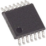
| 产品图片 |
|
| rohs | 符合RoHS无铅 / 符合限制有害物质指令(RoHS)规范要求 |
| 产品系列 | 放大器 IC,精密放大器,Analog Devices AD8668ARUZ- |
| 数据手册 | |
| 产品型号 | AD8668ARUZ |
| 产品培训模块 | http://www.digikey.cn/PTM/IndividualPTM.page?site=cn&lang=zhs&ptm=30008http://www.digikey.cn/PTM/IndividualPTM.page?site=cn&lang=zhs&ptm=26202 |
| 产品目录页面 | |
| 产品种类 | 精密放大器 |
| 供应商器件封装 | 14-TSSOP |
| 共模抑制比—最小值 | 110 dB |
| 关闭 | No |
| 包装 | 管件 |
| 压摆率 | 3.5 V/µs |
| 双重电源电压 | 2.5 V to 8 V |
| 可用增益调整 | 108 dB |
| 商标 | Analog Devices |
| 增益带宽生成 | 4 MHz |
| 增益带宽积 | 4MHz |
| 安装类型 | 表面贴装 |
| 安装风格 | SMD/SMT |
| 封装 | Tube |
| 封装/外壳 | 14-TSSOP(0.173",4.40mm 宽) |
| 封装/箱体 | TSSOP-14 |
| 工作温度 | -40°C ~ 125°C |
| 工作电源电压 | 5 V to 16 V |
| 工厂包装数量 | 96 |
| 放大器类型 | 通用 |
| 最大双重电源电压 | 8 V |
| 最大工作温度 | + 125 C |
| 最小双重电源电压 | 2.5 V |
| 最小工作温度 | - 40 C |
| 标准包装 | 96 |
| 电压-电源,单/双 (±) | 5 V ~ 16 V, ±2.5 V ~ 8 V |
| 电压-输入失调 | 600µV |
| 电压增益dB | 103.23 dB |
| 电流-电源 | 1.15mA |
| 电流-输入偏置 | 0.2pA |
| 电流-输出/通道 | 140mA |
| 电源电压-最大 | 16 V |
| 电源电压-最小 | 5 V |
| 电源电流 | 1.15 mA |
| 电源类型 | Single, Dual |
| 电路数 | 4 |
| 系列 | AD8668 |
| 视频文件 | http://www.digikey.cn/classic/video.aspx?PlayerID=1364138032001&width=640&height=505&videoID=2245193153001http://www.digikey.cn/classic/video.aspx?PlayerID=1364138032001&width=640&height=505&videoID=2245193159001 |
| 转换速度 | 3.5 V/us |
| 输入偏压电流—最大 | 550 pA |
| 输入电压范围—最大 | 14 V |
| 输入补偿电压 | 600 uV |
| 输出类型 | Rail to Rail Output |
| 通道数量 | 4 Channel |


- 商务部:美国ITC正式对集成电路等产品启动337调查
- 曝三星4nm工艺存在良率问题 高通将骁龙8 Gen1或转产台积电
- 太阳诱电将投资9.5亿元在常州建新厂生产MLCC 预计2023年完工
- 英特尔发布欧洲新工厂建设计划 深化IDM 2.0 战略
- 台积电先进制程称霸业界 有大客户加持明年业绩稳了
- 达到5530亿美元!SIA预计今年全球半导体销售额将创下新高
- 英特尔拟将自动驾驶子公司Mobileye上市 估值或超500亿美元
- 三星加码芯片和SET,合并消费电子和移动部门,撤换高东真等 CEO
- 三星电子宣布重大人事变动 还合并消费电子和移动部门
- 海关总署:前11个月进口集成电路产品价值2.52万亿元 增长14.8%


PDF Datasheet 数据手册内容提取
16 V, 4 MHz RR0 Amplifiers AD8665/AD8666/AD8668 FEATURES PIN CONFIGURATIONS Offset voltage: 2.5 mV max Low input bias current: 1 pA max OUT 1 5 V+ AD8665 Single-supply operation: 5 V to 16 V V– 2 TOP VIEW (Not to Scale) LDouwa ln-souipsep:l 8y onpVe/√raHtzio @n :1 ±02 k.5H Vz to ±8 V +IN 3 4 –IN 06195-039 Wide bandwidth: 4 MHz Figure 1. AD8665, 5-Lead SOT-23 (RJ-5) Rail-to-rail output Unity-gain stable NC 1 8 NC Lead-free packaging –IN 2 AD8665 7 VCC AD8666/AD8668 qualified for automotive applications +IN 3 TOPVIEW 6 OUT APPLICATIONS VEE 4NC( N= oNtOto CSOcNaNleE)CT5 NC 06195-040 Sensor amplification Figure 2. AD8665, 8-Lead SOIC_N (R-8) Reference buffers Medical equipment OUTA 1 8 V+ Physiological measurements –INA 2 AD8666 7 OUTB SCiognnsaulm filetre arsu adniod conditioning +INVA– 34 (NToOtPtoVSIEcaWle) 65 +–IINNBB 06018-001 Photodiode amplification Figure 3. AD8666, 8-Lead SOIC_N (R-8) ADC driver Level shifting circuits OUTA 1 8 V+ –INA 2 AD8666 7 OUTB GENERAL DESCRIPTION The AD866x family is single supply, rail-to-rail output +INVA– 34 (NToOtPtoVSIEcaWle) 65 +–IINNBB 06195-002 amplifiers with low noise performance featuring an extended Figure 4. AD8666, 8-Lead MSOP (RM-8) operating range with supply voltages up to 16 V. They also feature low input bias currents, wide signal bandwidth, and low OUTA 1 14 OUTD input voltage and current noise. For lower offset voltage, choose INA 2 13 –IND the AD8661/AD8662/AD8664 family. +INA 3 AD8668 12 +IND TOPVIEW The combination of low offsets, very low input bias currents, V+ 4 (NottoScale) 11 V– and wide supply range make these amplifiers useful in a wide +INB 5 10 +INC variety of cost sensitive applications normally associated with –INB 6 9 –INC much higher priced JFET amplifiers. Systems using high OUTB 7 8 OUTC 06195-003 impedance sensors, such as photo diodes, benefit from the Figure 5. AD8668, 14-Lead TSSOP (RU-14) combination of low input bias current, low noise, and low offset and bandwidth. The wide operating voltage range matches high OOUUTTAA 1 14 OUTD performance ADCs and DACs. Audio applications and medical –INA 2 13 –IND monitoring equipment can take advantage of the high input +INA 3 AAAADDDD8888666646468888 12 +IND impedance, low voltage and current noise, wide bandwidth, and V+ 4 TTTTOOOOPPPPVVVVIIIIEEEEWWWW 11 V– the lack of popcorn noise found in many other low input bias +INB 5 ((((NNNNoooottttttttooooSSSSccccaaaalllleeee)))) 10 +INC current amplifiers. O–UINTBB 67 98 O–IUNTCC 06195-004 The AD866x family is specified over the extended industrial Figure 6. AD8668, 14-Lead SOIC_N (R-14) temperature range (−40°C to +125°C). See the Ordering Guide for automotive models. Rev. B Information furnished by Analog Devices is believed to be accurate and reliable. However, no responsibility is assumed by Analog Devices for its use, nor for any infringements of patents or other One Technology Way, P.O. Box 9106, Norwood, MA 02062-9106, U.S.A. rights of third parties that may result from its use. Specifications subject to change without notice. No license is granted by implication or otherwise under any patent or patent rights of Analog Devices. Tel: 781.329.4700 www.analog.com Trademarks and registered trademarks are the property of their respective owners. Fax: 781.461.3113 ©2006–2011 Analog Devices, Inc. All rights reserved.
AD8665/AD8666/AD8668 TABLE OF CONTENTS Features .............................................................................................. 1 Absolute Maximum Ratings ............................................................5 Applications ....................................................................................... 1 Thermal Resistance .......................................................................5 General Description ......................................................................... 1 ESD Caution...................................................................................5 Pin Configurations ........................................................................... 1 Typical Performance Characteristics ..............................................6 Revision History ............................................................................... 2 Outline Dimensions ....................................................................... 12 Specifications ..................................................................................... 3 Ordering Guide .......................................................................... 14 REVISION HISTORY 7/11—Rev. A to Rev. B Change to Features and General Description Sections ............... 1 Updated Outline Dimensions ....................................................... 12 Changes to Ordering Guide .......................................................... 13 Added Automotive Products Section........................................... 13 10/06—Rev. 0 to Rev. A Added AD8665 ................................................................... Universal Added New Figure 1 and Figure 2, Renumbered Sequentially ................................................................ 1 Changes to Table 4 ............................................................................ 5 Changes to Figure 8, Figure 9, and Figure 11 ............................... 6 Change to Figure 40 ....................................................................... 11 Updated Outline Dimensions ....................................................... 12 Changes to Ordering Guide .......................................................... 13 4/06—Rev 0: Initial Version Rev. B | Page 2 of 16
AD8665/AD8666/AD8668 SPECIFICATIONS V = 5.0 V, V = V /2, T = 25oC, unless otherwise noted. DD CM DD A Table 1. Parameter Symbol Conditions Min Typ Max Unit INPUT CHARACTERISTICS Offset Voltage V V = 2.5 V 0.7 2.5 mV OS CM V = −0.1 V to +3.0 V 3.0 mV CM −40°C < T < +125°C 5.0 mV A Offset Voltage Drift ΔV /ΔT −40°C < T < +125°C 3.0 10 μV/°C OS A Input Bias Current I 0.2 1 pA B −40°C < T < +125°C 550 pA A Input Offset Current I 0.1 0.5 pA OS −40°C < T < +125°C 70 pA A Input Voltage Range V −0.1 +3.0 V CM Common-Mode Rejection Ratio CMRR V = −0.1 V to +3.0 V 84 100 dB CM −40°C < T < +125°C 79 dB A Large-Signal Voltage Gain A R = 2 kΩ, V = 0.5 V to 4.5 V 68 145 V/mV VO L O OUTPUT CHARACTERISTICS Output Voltage High V I = 1 mA 4.88 4.93 V OH OUT −40°C < T < +125°C 4.86 V A Output Voltage Low V I = 1 mA 50 85 mV OL OUT −40°C < T < +125°C 105 mV A Short-Circuit Output Current I ±19 mA SC Closed-Loop Output Impedance Z At 1 MHz, A = 1 50 Ω OUT V POWER SUPPLY Power Supply Rejection Ratio PSRR V = 5.0 V to 16 V 98 115 dB DD −40°C < T < +125°C 94 dB A Supply Current per Amplifier I 1.1 1.4 mA SY −40°C < T < +125°C 2.0 mA A DYNAMIC PERFORMANCE Slew Rate SR R = 2 kΩ 3.5 V/μs L Gain Bandwidth Product GBP 4 MHz Phase Margin Φ 70 Degrees M NOISE PERFORMANCE Peak-to-Peak Noise e p-p 0.1 Hz to 10 Hz 2.4 μV p-p n Voltage Noise Density e f = 1 kHz 10 nV/√Hz n f = 10 kHz 8 nV/√Hz Channel Separation CS f = 10 kHz −115 dB Rev. B | Page 3 of 16
AD8665/AD8666/AD8668 V = 16 V, V = V /2, T = 25oC, unless otherwise noted. DD CM DD A Table 2. Parameter Symbol Conditions Min Typ Max Unit INPUT CHARACTERISTICS Offset Voltage V V = 8 V 0.6 2.5 mV OS CM V = −0.1 V to +14.0 V 3.0 mV CM −40°C < T < +125°C 5.0 mV A Offset Voltage Drift ΔV /ΔT −40°C < T < +125°C 3.0 10 μV/°C OS A Input Bias Current I 0.2 1 pA B −40°C < T < +125°C 550 pA A Input Offset Current I 0.1 0.5 pA OS −40°C < T < +125°C 70 pA A Input Voltage Range V −0.1 +14.0 V CM Common-Mode Rejection Ratio CMRR V = −0.1 V to +14.0 V 90 110 dB CM −40°C < T < +125°C 80 dB A Large-Signal Voltage Gain A R = 2 kΩ, V = 0.5 V to 15.5 V 130 255 V/mV VO L O OUTPUT CHARACTERISTICS Output Voltage High V I = 1 mA 15.94 15.96 V OH OUT −40°C < T < +125°C 15.90 V A Output Voltage Low V I = 1 mA 22 40 mV OL OUT −40°C < T < +125°C 50 mV A Short-Circuit Output Current I ±140 mA SC Closed-Loop Output Impedance Z At 1 MHz, A = 1 50 Ω OUT V POWER SUPPLY Power Supply Rejection Ratio PSRR V = 5.0 V to 16 V 98 115 dB DD −40°C < T < +125°C 94 dB A Supply Current per Amplifier I 1.15 1.55 mA SY −40°C < T < +125°C 2.0 mA A DYNAMIC PERFORMANCE Slew Rate SR R = 2 kΩ 3.5 V/μs L Gain Bandwidth Product GBP 4 MHz Phase Margin Φ 73 Degrees M NOISE PERFORMANCE Peak-to-Peak Noise e p-p 0.1 Hz to 10 Hz 2.5 μV p-p n Voltage Noise Density e f = 1 kHz 10 nV/√Hz n f = 10 kHz 8 nV/√Hz Channel Separation CS f = 10 kHz −115 dB Rev. B | Page 4 of 16
AD8665/AD8666/AD8668 ABSOLUTE MAXIMUM RATINGS THERMAL RESISTANCE Table 3. Parameter Rating Table 4. Thermal Resistance Supply Voltage 18 V Package Type θJA θJC Unit Input Voltage GND to VDD 5-Lead SOT-23 (RJ-5) 240 92 °C/W Differential Input Voltage ±18 V 8-Lead SOIC_N (R-8) 158 43 °C/W Output Short-Circuit to GND Indefinite 8-Lead MSOP (RM-8) 210 45 °C/W Storage Temperature Range −65°C to +150°C 14-Lead SOIC (R-14) 120 36 °C/W Operating Temperature Range −40°C to +125°C 14-Lead TSSOP (RU-14) 180 35 °C/W Lead Temperature (Soldering, 60 sec) 300°C Junction Temperature 150°C ESD CAUTION Stresses above those listed under Absolute Maximum Ratings may cause permanent damage to the device. This is a stress rating only; functional operation of the device at these or any other conditions above those indicated in the operational section of this specification is not implied. Exposure to absolute maximum rating conditions for extended periods may affect device reliability. Rev. B | Page 5 of 16
AD8665/AD8666/AD8668 TYPICAL PERFORMANCE CHARACTERISTICS 100 300 VDD = 16V VS = 5V AND 16V 90 VCM = 8V TA = 25°C 250 80 600AMPLIFIERS S A) MPLIFIER 7600 RRENT (p200 F A 50 CU150 O S ER 40 BIA NUMB 30 NPUT 100 I 20 50 10 0–3 –2 INPU–T1 OFFSET0 VOLTAGE1 (mV) 2 3 06195-005 0–40 –20 0 T2E0MPER4A0TURE6 (0°C) 80 100 120 06195-008 Figure 7. Input Offset Voltage Distribution Figure 10. Input Bias Current vs. Temperature 20 10000 VDD = 16V VDD = 16V 18 V–4C0M° C= <8VTA< +125°C mV) TA = 25°C 16 300 AMPLIFIERS E (1000 ERS 14 TAG VSDODU TROC IVNOGH F AMPLIFI 1120 TION VOL 100 VSOINLKING O A BER 8 ATUR 10 NUM 6 UT S 4 TP 1 U O 2 0 0.1 0 1 2 3 4 T5CVOS6 (µV/°7C) 8 9 10 11 12 06195-006 0.001 0.01 LOA0.D1 CURRENT 1(mA) 10 100 06195-009 Figure 8. VOS Drift (TCVOS) Distribution Figure 11. Output Saturation Voltage vs. Load Current 5 100 VDD = 16V VDD = 16V 4 TA= 25°C V) IOUT = 1mA m V) 3 E ( 80 m G E ( 2 TA G L A O FSET VOLT –110 URATION V 6400 VSDODU TROC IVNOGH F T O A INPUT ––23 OUTPUT S 20 VSOINLKING –4 –5–1 0 1 2INP3UT 4COM5MO6N-M7OD8E VO9LT1A0GE1 1(V)12 13 14 15 06195-007 0–40 –20 0 T2E0MPER4A0TURE6 (0°C) 80 100 120 06195-010 Figure 9. Offset Voltage vs. Common-Mode Voltage Figure 12. Output Saturation Voltage vs. Temperature Rev. B | Page 6 of 16
AD8665/AD8666/AD8668 80 0 100 VDD = 16V VDD = 16V RL = 2kΩ TA = 25°C CL = 10pF es) 60 45 e 80 gr B) De N (d PHASE FT ( OOP GAI 40 90 HASE SHI SRR (dB) 60 N-L 20 GAIN ФM = 73° 135 P P P 40 E O OP LO N- 0 180 PE 20 PSRR– O PSRR+ –20 225 0 1k 10k FREQU1E0N0kCY (Hz) 1M 10M 06195-011 1k 10k FREQUEN1C0Y0 k(Hz) 1M 4M 06195-014 Figure 13. Open-Loop Gain and Phase vs. Frequency Figure 16. Power Supply Rejection Ratio vs. Frequency 1000 100 VDD = 16V VDD = 5V TO 16V TA = 25°C 100 V/√Hz) n Y ( Ω) 10 AV = +100 ENSIT (OUT AV = +10 AV = +1 SE D 10 Z 1 NOI E G A T L 0.1 O V 0.01 1 100 1k F1R0EkQUENCY1 (0H0zk) 1M 10M 06195-012 10 100FREQUENCY (Hz)1k 10k 06195-015 Figure 14. Closed-Loop Output Impedance vs. Frequency Figure 17. Voltage Noise Density vs. Frequency 120 VDD = 16V VDD = 5V TO 16V TA = 25°C TA = 25°C 100 V) 80 DI CMRR (dB) 60 LTAGE (1µV/ O 40 V 20 01k 10k FREQUEN1C0Y0 k(Hz) 1M 4M 06195-013 TIME (1s/DIV) 06195-016 Figure 15. Common-Mode Rejection Ratio vs. Frequency Figure 18. 0.1 Hz to 10 Hz Voltage Noise Rev. B | Page 7 of 16
AD8665/AD8666/AD8668 VDD = 16V RL = 10kΩ 0V CL = 10pF VDD = ±8V AV = +1 AV = –100 DIV) –100mV VIN V/ m 0 8V (2UT VOUT O V 0V TIME (0.5µs/DIV) 06195-017 TIME (5µs/DIV) 06195-020 Figure 19. Small-Signal Transient Response Figure 22. Positive Overload Recovery Time 10 VDD =±8V VDD = ±8V 8 CRLL == 1100kpΩF 100mV VIN AV = –100 6 AV = +1 4 2 0V V) (UT 0 0V O V –2 –4 –6 VOUT –8 –8V –10 TIME (2µs/DIV) 06195-018 TIME (5µs/DIV) 06195-021 Figure 20. Large-Signal Transient Response Figure 23. Negative Overload Recovery Time 70 80 VDD = 16V VDD = 5V VIN = 100mV p-p 70 VCM = 2.5V 60 TA = 25°C 550 AMPLIFIERS S 60 50 ER OT (%) 40 MPLIFI 50 HO +OS F A 40 S O OVER 30 –OS MBER 30 20 NU 20 10 10 01 LO10AD CAPACITANCE 1(p00F) 1000 06195-019 0–3 –2 INPU–T1 OFFSET0 VOLTAGE1 (mV) 2 3 06195-022 Figure 21. Small-Signal Overshoot vs. Load Capacitance Figure 24. Input Offset Voltage Distribution Rev. B | Page 8 of 16
AD8665/AD8666/AD8668 30 120 VDD = 5V VDD = 5V 25 V–4C0M° C= ≤2.T5AV≤ +125°C mV) 100 ILOAD = 1mA S 300 AMPLIFIERS GE ( VDD TO VOH R A SOURCING MPLIFIE 20 N VOLT 80 A O F 15 TI 60 O A MBER 10 SATUR 40 VSOINLKING NU UT P T 5 U 20 O 0 0 0 1 2 3 T4CVOS5 (µV/°C6) 7 8 9 10 06195-023 –40 –20 0 T2E0MPER4A0TURE6 (0°C) 80 100 120 06195-026 Figure 25. VOS Drift (TCVOS) Distribution Figure 28. Output Saturation Voltage vs. Temperature 5 80 0 VDD = 5V VDD = 5V 4 TA=25°C RCLL == 12k0pΩF es) ET VOLTAGE (mV) 3210 OOP GAIN (dB) 6400 PHASE 4950 HASE SHIFT (Degre PUT OFFS ––12 OPEN-L 20 GAIN ФM = 70° 135 N-LOOP P IN –3 0 180 PE O –4 –5–0.5 0 IN0P.5UT CO1M.0MON-M1.O5DE V2O.0LTAGE2. 5(V) 3.0 3.5 06195-024 –201k 10k FREQU1E0N0kCY (Hz) 1M 10M225 06195-027 Figure 26. Offset Voltage vs. Common-Mode Voltage Figure 29. Open-Loop Gain and Phase vs. Frequency 3000 VDD = 5V 1000 VDD = 5V V)1000 TA = 25°C m E ( 100 G A LT 100 URATION VO 10 VSDODU TROC IVNOGH VSOINLKING Z (Ω)OUT 101 AV = +100 AT AV = +10 S T U P 1 0.1 T U O AV = +1 0.01.001 0.01 LOAD C0U.1RRENT (mA)1 10 20 06195-025 0.01100 1k F1R0EkQUENCY1 (0H0zk) 1M 10M 06195-028 Figure 27. Output Saturation Voltage vs. Load Current Figure 30. Closed-Loop Output Impedance vs. Frequency Rev. B | Page 9 of 16
AD8665/AD8666/AD8668 120 1.5 VDD = 5V VDD =±2.5V 100 TA=25°C 1.0 CRLL == 1100kpΩF AV = +1 0.5 80 0 MRR (dB) 60 V (V)OUT–0.5 C –1.0 40 –1.5 20 –2.0 01k 10k FREQUEN1C0Y0 k(Hz) 1M 4M 06195-029 –2.5 TIME (1µs/DIV) 06195-032 Figure 31. Common-Mode Rejection Ratio vs. Frequency Figure 34. Large-Signal Transient Response 100 70 VDD = 5V VDD =5V TA=25°C VIN = 100mV p-p 60 80 50 %) dB) 60 OT ( 40 R ( HO +OS R S PS 40 ER 30 V O –OS 20 PSRR– 20 10 PSRR+ 0 0 1k 10k FREQUEN1C0Y0 k(Hz) 1M 4M 06195-030 1 LO10AD CAPACITANCE 1(p00F) 1000 06195-033 Figure 32. Power Supply Rejection Ratio vs. Frequency Figure 35. Small-Signal Overshoot vs. Load Capacitance VDD = 5V VDD =±2.5V RL = 100kΩ AV = –100 CL = 10pF 2.5V AV = +1 VOUT V) DI V/ m 0 0V 2 (UT O 0V V VIN –100mV TIME (0.4µs/DIV) 06195-031 TIME (4µs/DIV) 06195-034 Figure 33. Small-Signal Transient Response Figure 36. Positive Overload Recovery Time Rev. B | Page 10 of 16
AD8665/AD8666/AD8668 2.00 VDD =±2.5V AV = –100 1.75 100mV VIN mA)1.50 T (1.25 N E R 0V UR1.00 C 0V PLY 0.75 P U S 0.50 VOUT 0.25 –2.5V TIME (4µs/DIV) 06195-035 00 2 4 SU6PPLY VO8LTAGE10 (V) 12 14 16 06195-037 Figure 37. Negative Overload Recovery Time Figure 39. Supply Current vs. Supply Voltage 2.0 10 1.8 VOUT = VDD/2 8 VIN VADVD = =+±18V 1.6 6 VOUT mA) 1.4 4 LY CURRENT ( 110...208 VDD = 16V VDD = 5V VOLTAGE (V) –220 P P U 0.6 –4 S 0.4 –6 0.2 –8 0–40 –20 0 T2E0MPER4A0TURE6 (0°C) 80 100 120 06195-036 –10 TIME (10µs/DIV) 06195-038 Figure 38. Supply Current vs. Temperature Figure 40. No Output Phase Reversal Rev. B | Page 11 of 16
AD8665/AD8666/AD8668 OUTLINE DIMENSIONS 5.00(0.1968) 4.80(0.1890) 8 5 4.00(0.1574) 6.20(0.2441) 3.80(0.1497) 1 4 5.80(0.2284) 1.27(0.0500) 0.50(0.0196) BSC 1.75(0.0688) 0.25(0.0099) 45° 0.25(0.0098) 1.35(0.0532) 8° 0.10(0.0040) 0° COPLANARITY 0.51(0.0201) 0.10 SEATING 0.31(0.0122) 0.25(0.0098) 10..2470((00..00510507)) PLANE 0.17(0.0067) COMPLIANTTOJEDECSTANDARDSMS-012-AA C(RINOEFNPEATRRREOENNLCLTEIHNEOGSNDELISYM)AEANNRDSEIAORRNOESUNANORDETEDAIN-POMPFRIFLOLMPIMIRLELIATIMTEEERTFSEO;RIRNECUQHSUEDIVIINMAELDENENSSTIIOGSNNFS.OR 012407-A Figure 41. 8-Lead Standard Small Outline Package [SOIC_N] Narrow Body (R-8) Dimensions shown in millimeters and (inches) 3.20 3.00 2.80 8 5 5.15 3.20 4.90 3.00 4.65 2.80 1 4 PIN1 IDENTIFIER 0.65BSC 0.95 15°MAX 0.85 1.10MAX 0.75 0.80 0.15 0.40 6° 0.23 0.55 CO0P.0L50A.1N0ARICTOYMPLIANT0.T25OJEDECSTA0°NDARDS0M.0O9-187-AA 0.40 10-07-2009-B Figure 42. 8-Lead Mini Small Outline Package [MSOP] (RM-8) Dimensions shown in millimeters Rev. B | Page 12 of 16
AD8665/AD8666/AD8668 5.10 5.00 4.90 14 8 4.50 4.40 6.40 BSC 4.30 1 7 PIN 1 0.65 BSC 1.05 1.00 1M.A20X 0.20 0.80 0.09 0.75 0.15 8° 0.60 0.05 0.30 SPELAATNIENG 0° 0.45 COPLANARITY 0.19 0.10 COMPLIANT TO JEDEC STANDARDS MO-153-AB-1 061908-A Figure 43. 14-Lead Thin Shrink Small Outline Package [TSSOP] (RU-14) Dimensions shown in millimeters 8.75 (0.3445) 8.55 (0.3366) 4.00 (0.1575) 14 8 6.20 (0.2441) 3.80 (0.1496) 1 7 5.80 (0.2283) 1.27 (0.0500) 0.50 (0.0197) BSC 45° 1.75 (0.0689) 0.25 (0.0098) 0.25 (0.0098) 1.35 (0.0531) 8° 0.10 (0.0039) 0° COPLANARITY SEATING 0.10 0.51 (0.0201) PLANE 0.25 (0.0098) 1.27 (0.0500) 0.31 (0.0122) 0.17 (0.0067) 0.40 (0.0157) COMPLIANTTO JEDEC STANDARDS MS-012-AB C(RINOEFNPEATRRREOENNLCLTEIHN EOGSN EDLSIYM)AEANNRDSEI AORRNOESU NANORDEET DAIN-PO MPFRIFLO LMPIIMRLELIATIMTEEER TFSEO; RIRN ECUQHSU EDI VIINMA LEDENENSSTIIOGSN NFS.OR 060606-A Figure 44. 14-Lead Standard Small Outline Package [SOIC_N] Narrow Body (R-14) Dimensions shown in millimeters and (inches) Rev. B | Page 13 of 16
AD8665/AD8666/AD8668 3.00 2.90 2.80 1.70 5 4 3.00 1.60 2.80 1.50 2.60 1 2 3 0.95BSC 1.90 BSC 1.30 1.15 0.90 1.45MAX 0.20MAX 0.95MIN 0.08MIN 0.55 0.15MAX 10° 0.45 0.05MIN 0.50MAX SPELAATNIENG 5° B0S.6C0 0.35 0.35MIN 0° COMPLIANTTOJEDECSTANDARDSMO-178-AA 11-01-2010-A Figure 45. 5-Lead Small Outline Transistor Package [SOT-23] (RJ-5) Dimensions shown in millimeters ORDERING GUIDE Model1, 2 Temperature Range Package Description Package Option Branding AD8665ARZ −40°C to +125°C 8-Lead SOIC_N R-8 AD8665ARZ-REEL −40°C to +125°C 8-Lead SOIC_N R-8 AD8665ARZ-REEL7 −40°C to +125°C 8-Lead SOIC_N R-8 AD8665ARJZ-R2 −40°C to +125°C 5-Lead SOT-23 RJ-5 A1B AD8665ARJZ-REEL −40°C to +125°C 5-Lead SOT-23 RJ-5 A1B AD8665ARJZ-REEL7 −40°C to +125°C 5-Lead SOT-23 RJ-5 A1B AD8666ARZ −40°C to +125°C 8-Lead SOIC_N R-8 AD8666ARZ-REEL −40°C to +125°C 8-Lead SOIC_N R-8 AD8666ARZ-REEL7 −40°C to +125°C 8-Lead SOIC_N R-8 AD8666ARMZ −40°C to +125°C 8-Lead MSOP RM-8 A16 AD8666ARMZ-REEL −40°C to +125°C 8-Lead MSOP RM-8 A16 AD8666WARZ-R7 −40°C to +125°C 8-Lead SOIC_N R-8 AD8666WARZ-RL −40°C to +125°C 8-Lead SOIC_N R-8 AD8668ARZ −40°C to +125°C 14-Lead SOIC_N R-14 AD8668ARZ-REEL −40°C to +125°C 14-Lead SOIC_N R-14 AD8668ARZ-REEL7 −40°C to +125°C 14-Lead SOIC_N R-14 AD8668ARUZ −40°C to +125°C 14-Lead TSSOP RU-14 AD8668ARUZ-REEL −40°C to +125°C 14-Lead TSSOP RU-14 AD8668WARUZ-R7 −40°C to +125°C 14-Lead TSSOP RU-14 AD8668WARUZ-RL −40°C to +125°C 14-Lead TSSOP RU-14 1 Z = RoHS Compliant Model 2 W = Qualified for Automotive Applications. AUTOMOTIVE PRODUCTS The AD8666W/AD8668W models are available with controlled manufacturing to support the quality and reliability requirements of automotive applications. Note that these automotive models may have specifications that differ from the commercial models; therefore, designers should review the Specifications section of this data sheet carefully. Only the automotive grade products shown are available for use in automotive applications. Contact your local Analog Devices account representative for specific product ordering information and to obtain the specific Automotive Reliability reports for these models. Rev. B | Page 14 of 16
AD8665/AD8666/AD8668 NOTES Rev. B | Page 15 of 16
AD8665/AD8666/AD8668 NOTES ©2006–2011 Analog Devices, Inc. All rights reserved. Trademarks and registered trademarks are the property of their respective owners. D06195-0-7/11(B) Rev. B | Page 16 of 16