ICGOO在线商城 > 集成电路(IC) > 线性 - 放大器 - 仪表,运算放大器,缓冲器放大器 > AD8667ARMZ
 Datasheet下载
- 型号: AD8667ARMZ
- 制造商: Analog
- 库位|库存: xxxx|xxxx
- 要求:
| 数量阶梯 | 香港交货 | 国内含税 |
| +xxxx | $xxxx | ¥xxxx |
查看当月历史价格
查看今年历史价格
AD8667ARMZ产品简介:
ICGOO电子元器件商城为您提供AD8667ARMZ由Analog设计生产,在icgoo商城现货销售,并且可以通过原厂、代理商等渠道进行代购。 AD8667ARMZ价格参考。AnalogAD8667ARMZ封装/规格:线性 - 放大器 - 仪表,运算放大器,缓冲器放大器, 通用 放大器 2 电路 满摆幅 8-MSOP。您可以下载AD8667ARMZ参考资料、Datasheet数据手册功能说明书,资料中有AD8667ARMZ 详细功能的应用电路图电压和使用方法及教程。
AD8667ARMZ 是由 Analog Devices Inc.(亚德诺半导体公司)生产的一款低噪声、低功耗的精密运算放大器,属于线性放大器类别中的仪表、运算放大器和缓冲器放大器。它广泛应用于需要高精度、低失真和低功耗的场景。以下是其主要应用场景:

1. 工业自动化与控制
   - AD8667ARMZ 可用于工业传感器信号调理电路中,例如压力传感器、温度传感器或光电传感器。它的低噪声特性和高精度能够准确放大微弱信号,同时保持信号完整性。
   - 在可编程逻辑控制器 (PLC) 和数据采集系统中,该放大器可用于信号放大和滤波。

2. 医疗设备
   - 在医疗电子领域,如心电图 (ECG)、脑电图 (EEG) 或超声波设备中,AD8667ARMZ 的低噪声和低失调电压特性使其非常适合处理生物电信号。
   - 它还可以用于便携式医疗设备中,得益于其低功耗设计,延长电池寿命。

3. 通信系统
   - 用于射频 (RF) 和中频 (IF) 信号链中的增益级或缓冲级,确保信号不失真地传输。
   - 在通信基站或卫星接收器中,该放大器可以提高信号质量并减少干扰。

4. 消费类电子产品
   - 在音频设备中,AD8667ARMZ 可用作前置放大器,提供高质量的声音输出,同时保持低失真。
   - 在智能家居设备中,它可用于环境监测模块,如空气质量检测仪或湿度传感器。

5. 汽车电子
   - 在汽车传感器系统中,例如胎压监测系统 (TPMS) 或惯性测量单元 (IMU),该放大器可以精确放大传感器信号。
   - 它还适用于车载信息娱乐系统中的音频信号处理。

6. 测试与测量仪器
   - 在示波器、万用表或其他精密测量仪器中,AD8667ARMZ 的高精度和稳定性使其成为理想选择,用于放大和处理输入信号。

总之,AD8667ARMZ 凭借其低噪声、低功耗和高精度特性,适用于多种对信号质量要求较高的场景,特别是在需要小信号放大和长电池续航的应用中表现优异。
| 参数 | 数值 |
| -3db带宽 | - |
| 产品目录 | 集成电路 (IC)半导体 |
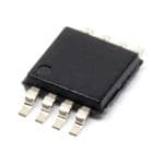
| 描述 | IC OPAMP GP 540KHZ RRO 8MSOP精密放大器 Low Noise Prec 16V CMOS RR Dual |
| 产品分类 | Linear - Amplifiers - Instrumentation, OP Amps, Buffer Amps集成电路 - IC |
| 品牌 | Analog Devices Inc |
| 产品手册 | |
| 产品图片 |
|
| rohs | 符合RoHS无铅 / 符合限制有害物质指令(RoHS)规范要求 |
| 产品系列 | 放大器 IC,精密放大器,Analog Devices AD8667ARMZDigiTrim® |
| 数据手册 | |
| 产品型号 | AD8667ARMZ |
| 产品培训模块 | http://www.digikey.cn/PTM/IndividualPTM.page?site=cn&lang=zhs&ptm=30008http://www.digikey.cn/PTM/IndividualPTM.page?site=cn&lang=zhs&ptm=26202 |
| 产品种类 | 精密放大器 |
| 供应商器件封装 | 8-MSOP |
| 共模抑制比—最小值 | 109 dB |
| 关闭 | No |
| 包装 | 管件 |
| 压摆率 | 0.3 V/µs |
| 双重电源电压 | 2.5 V to 8 V |
| 可用增益调整 | 140 dB |
| 商标 | Analog Devices |
| 增益带宽生成 | 540 kHz |
| 增益带宽积 | 540kHz |
| 安装类型 | 表面贴装 |
| 安装风格 | SMD/SMT |
| 封装 | Tube |
| 封装/外壳 | 8-TSSOP,8-MSOP(0.118",3.00mm 宽) |
| 封装/箱体 | MSOP-8 |
| 工作温度 | -40°C ~ 125°C |
| 工作电源电压 | 5 V to 16 V |
| 工厂包装数量 | 50 |
| 放大器类型 | 通用 |
| 最大双重电源电压 | 8 V |
| 最大工作温度 | + 125 C |
| 最小双重电源电压 | 2.5 V |
| 最小工作温度 | - 40 C |
| 标准包装 | 50 |
| 电压-电源,单/双 (±) | 5 V ~ 16 V, ±2.5 V ~ 8 V |
| 电压-输入失调 | 40µV |
| 电压增益dB | 140 dB |
| 电流-电源 | 230µA |
| 电流-输入偏置 | 0.3pA |
| 电流-输出/通道 | 50mA |
| 电源电压-最大 | 16 V |
| 电源电压-最小 | 5 V |
| 电源电流 | 230 uA |
| 电源类型 | Single |
| 电路数 | 2 |
| 系列 | AD8667 |
| 视频文件 | http://www.digikey.cn/classic/video.aspx?PlayerID=1364138032001&width=640&height=505&videoID=2245193153001http://www.digikey.cn/classic/video.aspx?PlayerID=1364138032001&width=640&height=505&videoID=2245193159001 |
| 转换速度 | 0.3 V/us |
| 输入偏压电流—最大 | 120 pA |
| 输入电压范围—最大 | 14.5 V |
| 输入补偿电压 | 40 uV |
| 输出类型 | 满摆幅 |
| 通道数量 | 2 Channel |


- 商务部:美国ITC正式对集成电路等产品启动337调查
- 曝三星4nm工艺存在良率问题 高通将骁龙8 Gen1或转产台积电
- 太阳诱电将投资9.5亿元在常州建新厂生产MLCC 预计2023年完工
- 英特尔发布欧洲新工厂建设计划 深化IDM 2.0 战略
- 台积电先进制程称霸业界 有大客户加持明年业绩稳了
- 达到5530亿美元!SIA预计今年全球半导体销售额将创下新高
- 英特尔拟将自动驾驶子公司Mobileye上市 估值或超500亿美元
- 三星加码芯片和SET,合并消费电子和移动部门,撤换高东真等 CEO
- 三星电子宣布重大人事变动 还合并消费电子和移动部门
- 海关总署:前11个月进口集成电路产品价值2.52万亿元 增长14.8%


PDF Datasheet 数据手册内容提取
Low Noise, Precision, 16 V, CMOS, Rail-to-Rail Operational Amplifiers Data Sheet AD8663/AD8667/AD8669 FEATURES PIN CONFIGURATIONS Low offset voltage: 175 μV maximum @ VSY = 5 V AD8663 Low supply current: 275 μA maximum per amplifier TOP VIEW (Not to Scale) Single-supply operation: 5 V to 16 V Low noise: 23 nV/√Hz NC 1 8 NC NC 1 8 NC –IN 2 AD8663 7 V+ –IN 2 7 V+ Low input bias current: 300 fA TOP VIEW +IN 3 (Not to Scale) 6 OUT +IN 3 6 OUT Unity-gain stable Sm3a mll mpa ×ck 3a mgems ,a 8v-aleilaadb lLeF CSP V– N4C = NO CONNECT5 NC 06742-001 N1.ONTVCE– S=4 NO CONNECT. DO N5OTNC Ot8h-eler apda cMkSaOgePs 2.CVC–OO NONNNREE LCCETTA TTVOHEE TIT EH UXISNP POCIOSNEN.DN EPCATDE TDO. 06742-002 Figure 1. 8-Lead SOIC (R-8) Figure 2. 8-Lead LFCSP (CP-8-13) 8-lead SOIC 14-lead SOIC 14-lead TSSOP OUTA 11 1144 OUTD APPLICATIONS –INA 22 1133 –IND OUT A 1 8 V+ Sensor front ends –IN A 2 AD8667 7 OUT B +INA 33 AADD88664698 1122 +IND TOP VIEW V+ 44 TTOOPPVVIIEEWW 1111 V– TEPLrolheawocntt sporioomdmwipoeedertde eA araD namcCpep pd lalirifmicivcapeatrltiisoifo inensr s +INV A– 34 (Not to Scale) 65 –+IINN BB 06742-003 O+–UIINNTBBB 567567 ((NNoottttooSSccaallee)) 11989800 +–OIIUNNTCCC 06742-004 Figure 3. 8-Lead MSOP (RM-8), Figure 4. 14-Lead SOIC (R-14), Medical diagnostic instruments 8-Lead SOIC (R-8) 14-Lead TSSOP (RU-14) pH and ORP meters and probes DAC or REF buffers GENERAL DESCRIPTION The AD8663/AD8667/AD8669 are rail-to-rail output amplifiers frequency data converters. The low bias current drift is well- that use the Analog Devices, Inc., patented DigiTrim® trimming suited for precision I-to-V converters. The combination of technique to achieve low offset voltage. The AD8663/AD8667/ precision offset, offset drift, and low noise also make the op AD8669 feature an extended operating range with supply amps ideal for gain, dc offset adjust, and active filter in both voltages up to 16 V. They also feature low input bias current, instrumentation and medical applications. These low power low input offset voltage, and low current noise. op amps can be used in IR thermometers, pH and ORP instru- ments, pressure transducer front ends, and other sensor signal The combination of low offset, very low input bias current, and conditioning circuits that are used in remote or wireless a wide supply range makes these amplifiers useful in a wide variety applications. of applications usually associated with higher priced JFET ampli- fiers. Systems using high impedance sensors, such as photodiodes, The AD8663/AD8667/AD8669 are specified over the extended benefit from the combination of low input bias current, low industrial temperature range of −40°C to +125°C. The single noise, low offset, and wide bandwidth. AD8663 is available in a narrow 8-lead SOIC package and a very thin, 8-lead LFCSP. The dual AD8667 is available in a narrow The ability to operate the device for single (5 V to 16 V) or dual 8-lead SOIC package and an 8-lead MSOP. The quad AD8669 supplies (±2.5 V to ±8 V) supports many applications. The rail- is available in a 14-lead SOIC and 14-lead small TSSOP. to-rail outputs provide increased dynamic range to drive low Rev. D Document Feedback Information furnished by Analog Devices is believed to be accurate and reliable. However, no responsibility is assumed by Analog Devices for its use, nor for any infringements of patents or other One Technology Way, P.O. Box 9106, Norwood, MA 02062-9106, U.S.A. rights of third parties that may result from its use. Specifications subject to change without notice. No license is granted by implication or otherwise under any patent or patent rights of Analog Devices. Tel: 781.329.4700 ©2007–2016 Analog Devices, Inc. All rights reserved. Trademarks and registered trademarks are the property of their respective owners. Technical Support www.analog.com
AD8663/AD8667/AD8669 Data Sheet TABLE OF CONTENTS Features .............................................................................................. 1 Absolute Maximum Ratings ............................................................5 Applications ....................................................................................... 1 Thermal Resistance .......................................................................5 Pin Configurations ........................................................................... 1 ESD Caution...................................................................................5 General Description ......................................................................... 1 Typical Performance Characteristics ..............................................6 Revision History ............................................................................... 2 Outline Dimensions ....................................................................... 13 Specifications ..................................................................................... 3 Ordering Guide .......................................................................... 15 Electrical Characteristics ............................................................. 3 REVISION HISTORY 5/2016—Rev. C to Rev. D 10/2007—Rev. 0 to Rev. A Changed CP-8-2 to CP-8-13 ........................................ Throughout Added AD8667 and AD8669 ............................................ Universal Changes to Figure 2 .......................................................................... 1 Changes to Features .......................................................................... 1 Changes to Table 4 ............................................................................ 5 Changes to General Description ..................................................... 1 Updated Outline Dimensions ....................................................... 13 Inserted Figure 3 and Figure 4 ......................................................... 1 Changes to Ordering Guide .......................................................... 15 Changes to Table 1, Power Supply Section ..................................... 3 Changes to Table 2 ............................................................................. 4 4/2013—Rev. B to Rev. C Reformatted Typical Performance Characteristics Section ......... 6 Changes to Figure 2 .......................................................................... 1 Changes to Figure 5 ........................................................................... 6 Added Exposed Pad Notation to Outline Dimensions ............. 14 Changes to Figure 13 ......................................................................... 7 Changes to Ordering Guide .......................................................... 15 Changes to Figure 17 and Figure 20 ............................................... 8 Inserted Figure 35 through Figure 39 .......................................... 11 1/2008—Rev. A to Rev. B Inserted Figure 40 and Figure 41 .................................................. 12 Added TSSOP ..................................................................... Universal Updated Outline Dimensions ....................................................... 13 Change to Table 4 ............................................................................. 5 Changes to Ordering Guide .......................................................... 15 Changes to Figure 8 and Figure 9 ................................................... 6 Changes to Figure 23 and Figure 26 ............................................... 9 7/2007—Revision 0: Initial Version Updated Outline Dimensions ....................................................... 13 Changes to Ordering Guide .......................................................... 15 Rev. D | Page 2 of 15
Data Sheet AD8663/AD8667/AD8669 SPECIFICATIONS ELECTRICAL CHARACTERISTICS V = 5.0 V, V = V /2, T = 25°C, unless otherwise noted. SY CM SY A Table 1. Parameter Symbol Conditions Min Typ Max Unit INPUT CHARACTERISTICS Offset Voltage V V = V /2 30 175 µV OS CM SY −40°C < T < +125°C 450 µV A Input Bias Current I 0.3 pA B −40°C < T < +85°C 45 pA A −40°C < T < +125°C 105 pA A Input Offset Current I 0.2 pA OS −40°C < T < +85°C 35 pA A −40°C < T < +125°C 65 pA A Input Voltage Range 0.2 3.0 V Common-Mode Rejection Ratio CMRR V = 0.2 V to 3.0 V 76 100 dB CM −40°C < T < +125°C 76 100 dB A Large Signal Voltage Gain A R = 100 kΩ, V = 0.5 V to 4.5 V 115 140 dB VO L OUT R = 2 kΩ, V = 0.5 V to 4.5 V 106 114 dB L OUT Offset Voltage Drift TCV −40°C < T < +125°C 1.5 5 µV/°C OS A OUTPUT CHARACTERISTICS Output Voltage High V I = 100 µA 4.95 4.97 V OH L −40°C < T < +125°C 4.90 V A Output Voltage High V I = 1 mA 4.65 4.80 V OH L −40°C < T < +125°C 4.60 V A Output Voltage Low V I = 100 µA 17 25 mV OL L −40°C < T < +125°C 35 mV A Output Voltage Low V I = 1 mA 150 200 mV OL L −40°C < T < +125°C 250 mV A Short-Circuit Current I ±7 mA SC Closed-Loop Output Impedance Z f = 100 kHz, A = 1 120 Ω OUT V POWER SUPPLY Power Supply Rejection Ratio PSRR V = 5 V to 16 V 95 105 dB SY −40°C < T < +125°C 95 dB A Supply Current per Amplifier I V = V /2 210 275 μA SY OUT SY −40°C < T < +125°C 325 μA A DYNAMIC PERFORMANCE Slew Rate SR R = 2 kΩ 0.26 V/µs L Gain Bandwidth Product GBP C = 20 pF 520 kHz L Phase Margin Φ C = 20 pF 60 Degrees M L NOISE PERFORMANCE Peak-to-Peak Noise e p-p f = 0.1 Hz to 10 Hz 2.5 µV p-p n Voltage Noise Density en f = 1 kHz 23 nV/√Hz f = 10 kHz 21 nV/√Hz Current Noise Density i f = 1 kHz 0.05 pA/√Hz n Rev. D | Page 3 of 15
AD8663/AD8667/AD8669 Data Sheet V = 16.0 V, V = V /2, T = 25°C, unless otherwise noted. SY CM SY A Table 2. Parameter Symbol Conditions Min Typ Max Unit INPUT CHARACTERISTICS Offset Voltage V V = V /2 40 300 µV OS CM SY −40°C < T < +125°C 500 µV A Input Bias Current I 0.3 pA B −40°C < T < +85°C 45 pA A −40°C < T < +125°C 120 pA A Input Offset Current I 0.2 pA OS −40°C < T < +85°C 35 pA A −40°C < T < +125°C 65 pA A Input Voltage Range 0.2 14.5 V Common-Mode Rejection Ratio CMRR V = 0.2 V to 14.5 V 87 109 dB CM −40°C < T < +125°C 87 109 dB A Large Signal Voltage Gain A R = 100 kΩ, V = 0.5 V to 15.5 V 115 140 dB VO L OUT R = 2 kΩ, V = 0.5 V to 15.5 V 106 111 dB L OUT Offset Voltage Drift TCV −40°C < T < +125°C 1.5 5 µV/°C OS A OUTPUT CHARACTERISTICS Output Voltage High V I = 100 μA 15.95 15.98 V OH L −40°C < T < +125°C 15.90 V A Output Voltage High V I = 1 mA 15.85 15.92 V OH L −40°C < T < +125°C 15.80 V A Output Voltage Low V I = 100 μA 17 25 mV OL L −40°C < T < +125°C 35 mV A Output Voltage Low V I = 1 mA 70 100 mV OL L −40°C < T < +125°C 125 mV A Short-Circuit Current I ±50 mA SC Closed-Loop Output Impedance Z f = 100 kHz, A = 1 100 Ω OUT V POWER SUPPLY Power Supply Rejection Ratio PSRR V = 5 V to 16 V 95 105 dB SY −40°C < T < +125°C 95 dB A Supply Current per Amplifier I V = V /2 230 285 μA SY OUT SY −40°C < T < +125°C 355 μA A DYNAMIC PERFORMANCE Slew Rate SR R = 2 kΩ 0.3 V/µs L Gain Bandwidth Product GBP C = 20 pF 540 kHz L Phase Margin Φ C = 20 pF 64 Degrees M L NOISE PERFORMANCE Peak-to-Peak Noise e p-p f = 0.1 Hz to 10 Hz 2.5 µV p-p n Voltage Noise Density en f = 1 kHz 23 nV/√Hz f = 10 kHz 21 nV/√Hz Current Noise Density i f = 1 kHz 0.05 pA/√Hz n Rev. D | Page 4 of 15
Data Sheet AD8663/AD8667/AD8669 ABSOLUTE MAXIMUM RATINGS THERMAL RESISTANCE Table 3. Parameter Rating θ is specified for the worst-case conditions, that is, a device JA Supply Voltage 18 V soldered in a circuit board for surface-mount packages. Input Voltage −0.1 V to V SY Table 4. Thermal Resistance Differential Input Voltage 18 V Package Type θ θ Unit Output Short-Circuit Duration to GND Indefinite JA JC 8-Lead SOIC (R-8) 121 43 °C/W Storage Temperature Range −60°C to +150°C 8-Lead LFCSP (CP-8-13) 751 181 °C/W Operating Temperature Range −40°C to +125°C 8-Lead MSOP (RM-8) 145 45 °C/W Junction Temperature Range −65°C to +150°C 14-Lead SOIC (R-14) 90 45 °C/W Lead Temperature, Soldering (60 sec) 300°C 14-Lead TSSOP (RU-14) 180 35 °C/W Stresses at or above those listed under Absolute Maximum Ratings may cause permanent damage to the product. This is a 1 Exposed pad soldered to application board. stress rating only; functional operation of the product at these ESD CAUTION or any other conditions above those indicated in the operational section of this specification is not implied. Operation beyond the maximum operating conditions for extended periods may affect product reliability. Rev. D | Page 5 of 15
AD8663/AD8667/AD8669 Data Sheet TYPICAL PERFORMANCE CHARACTERISTICS 1600 10000 VSY = 5V VSY = 16V 1400 –0.1V<VCM<+3.5V 9000 –0.1V<VCM<+14V TA=25°C 8000 TA=25°C S1200 S ER ER7000 FI FI PLI1000 PLI6000 M M A A F 800 F 5000 O O ER 600 ER 4000 B B UM UM3000 N 400 N 2000 200 1000 0–250 –200 –150 –100 –50VOS0(µV)50 100 150 200 250 06742-005 0–250 –200 –150 –100 –50VOS0(µV)50 100 150 200 250 06742-037 Figure 5. Input Offset Voltage Distribution Figure 8. Input Offset Voltage Distribution 40 40 VSY = ±2.5V VSY = ±8V 35 –40°C< TA<+125°C 35 –40°C<TA<+125°C RS30 RS30 E E PLIFI25 PLIFI25 M M OF A20 OF A20 R R BE15 BE15 M M U U N10 N10 5 5 0 0 1 2TCVOS (µV)3 4 5 06742-006 0 0 1 T2CVOS(µV/°C3) 4 5 06742-038 Figure 6. Offset Voltage Drift Distribution Figure 9. Offset Voltage Drift Distribution 500 300 VSY = 5V VSY = 16V 400 TA = 25°C 250 TA = 25°C 200 300 150 200 100 V) 100 V) 50 µ µ (S 0 (S 0 O O V–100 V –50 –100 –200 –150 –300 –200 –400 –250 –5000 0.5 1.0 1.5 2.0 VC2M.5 (V) 3.0 3.5 4.0 4.5 5.0 06742-007 –3000 2 4 6 VCM8 (V) 10 12 14 16 06742-010 Figure 7. Input Offset Voltage vs. Common-Mode Voltage Figure 10. Input Offset Voltage vs. Common-Mode Voltage Rev. D | Page 6 of 15
Data Sheet AD8663/AD8667/AD8669 100 100 VSY = 5V VSY = 16V TA = 125°C TA = 125°C 80 80 60 60 A) A) p p (B (B I I 40 40 20 20 00.5 1.0 1.5 2.0 VC2M. 5(V) 3.0 3.5 4.0 4.5 06742-013 00.5 2.5 4.5 6.5VCM 8(V.5) 10.5 12.5 14.5 06742-016 Figure 11. Input Bias Current vs. Common-Mode Voltage at 125°C Figure 14. Input Bias Current vs. Common-Mode Voltage at 125°C 100 100 VSY = 5V VSY = 16V 90 TA = 25°C 90 TA = 25°C 80 80 70 70 B) B) d d R ( 60 R ( 60 R R M M C C 50 50 40 40 30 30 20100 1k F1R0EkQUENCY1 (0H0zk) 1M 10M 06742-023 20100 1k F1R0EkQUENCY1 (0H0zk) 1M 10M 06742-039 Figure 12. CMRR vs. Frequency, VSY = 5 V Figure 15. CMRR vs. Frequency, VSY = 16 V 10000 10000 VSY = 5V VSY = 16V TA = 25°C TA = 25°C V) V) m m E ( 1000 E ( 1000 G G A A T T L L O O V 100 V 100 N VSY – VOH SOURCING N VSY – VOH SOURCING O O TI TI URA 10 VOL SINKING URA 10 VOL SINKING T T A A S S T T U U TP 1 TP 1 U U O O 0.01.001 0.01 LOAD CUR0.R1ENT (mA) 1 10 06742-011 0.01.001 0.01 LOA0.D1 CURRENT 1(mA) 10 100 06742-014 Figure 13. Output Swing Saturation Voltage vs. Load Current Figure 16. Output Swing Saturation Voltage vs. Load Current Rev. D | Page 7 of 15
AD8663/AD8667/AD8669 Data Sheet 350 140 300 120 VSY – VOH @ 1mA V) V) VSY – VOH @ 1mA m 250 m 100 E ( E ( G G A A T 200 T 80 L L VO VOL @ 1mA VO VOL @ 1mA UT 150 UT 60 O O P P RO 100 RO 40 D D 50 VOL @ 100µA 20 VOL @ 100µA VSY – VOH @ 100µA VSY – VOH @ 100µA 0 0 –40 –25 –10 5 T2E0MPE3R5ATU5R0E (°6C5) 80 95 110 125 06742-044 –40 –25 –10 5 T2E0MPE3R5ATU5R0E (°6C5) 80 95 110 125 06742-045 Figure 17. Output Voltage Saturation vs. Temperature Figure 20. Output Voltage Saturation vs. Temperature 120 120 100 100 s) 80 PHASE s) 80 PHASE e e e e egr 60 egr 60 D D E ( 40 E ( 40 AS GAIN CL = 0pF AS GAIN CL = 0pF H H P 20 P 20 D D N N A 0 A 0 B) B) N (d –20 N (d –20 GAI –40 GAI –40 CL = 200pF CL = 200pF –60 VSY = 5V –60 VSY = 16V TA = 25°C TA = 25°C –80 –80 100 1k F1R0EkQUENCY1 (0H0zk) 1M 10M 06742-017 100 1k F1R0EkQUENCY1 (0H0zk) 1M 10M 06742-020 Figure 18. Open-Loop Gain and Phase Shift vs. Frequency Figure 21. Open-Loop Gain and Phase Shift vs. Frequency 60 60 VSY = 5V VSY = 16V TA = 25°C TA = 25°C G = 100 G = 100 40 40 G = 10 G = 10 20 20 B) B) d d A (CL G = 1 A (CL G = 1 0 0 –20 –20 –40 –40 100 1k F1R0EkQUENCY1 (0H0zk) 1M 10M 06742-018 100 1k F1R0EkQUENCY1 (0H0zk) 1M 10M 06742-021 Figure 19. Closed-Loop Gain vs. Frequency Figure 22. Closed-Loop Gain vs. Frequency, VSY = 16 V Rev. D | Page 8 of 15
Data Sheet AD8663/AD8667/AD8669 1000 1000 G = 100 G = 100 100 G = 10 100 G = 10 VSY = 5V VSY = 16V TA = 25°C TA = 25°C G = 1 G = 1 Ω) Ω) (UT 10 (UT 10 O O Z Z 1 1 0.1 0.1 100 1k F1R0EkQUENCY1 (0H0zk) 1M 10M 06742-040 100 1k F1R0EkQUENCY1 (0H0zk) 1M 10M 06742-041 Figure 23. Closed-Loop Output Impedance vs. Frequency, VSY = 5 V Figure 26. Closed-Loop Output Impedance vs. Frequency, VSY = 16 V 90 90 VSY = 5V VSY = 16V 80 TA = 25°C 80 TA = 25°C 70 70 60 60 50 50 B) B) d 40 d 40 R ( R ( R 30 R 30 PS PSSR+ PS PSSR– 20 20 10 10 0 0 PSSR+ –10 PSSR– –10 –20 –20 100 1k F1R0EkQUENCY1 (0H0zk) 1M 10M 06742-024 100 1k F1R0EkQUENCY1 (0H0zk) 1M 10M 06742-027 Figure 24. PSRR vs. Frequency, VSY = 5 V Figure 27. PSRR vs. Frequency, VSY = 16 V 80 80 VSY = 5V VSY = 16V 70 TA = 25°C 70 TA = 25°C 60 60 T (%) 50 OS– T (%) 50 OS+ O O HO 40 HO 40 S S R R VE 30 OS+ VE 30 O O OS– 20 20 10 10 0 0 10 CAPACIT1A00NCE (pF) 1k 06742-025 10 CAPACIT1A00NCE (pF) 1k 06742-028 Figure 25. Small-Signal Overshoot vs. Load Capacitance, VSY = 5 V Figure 28. Small-Signal Overshoot vs. Load Capacitance, VSY = 16 V Rev. D | Page 9 of 15
AD8663/AD8667/AD8669 Data Sheet VSY = ±8V AV = 1 CL = 200pF RL = 2kΩ V) V/DI VSY = ±2.5V DIV) m AV = 1 V/ OLTAGE (200 CRLL == 220k0ΩpF VOLTAGE (2 V TIME (10µs/DIV) 06742-029 TIME (20µs/DIV) 06742-032 Figure 29. Large Signal Transient Response, VSY = ±2.5 V Figure 32. Large Signal Transient Response, VSY = ±8 V VSY = ±2.5V VSY = ±8V AV = 1 AV = 1 CL = 200pF CL = 200pF RL = 10kΩ RL = 10kΩ V) V) DI DI V/ V/ m m 0 0 5 5 E ( E ( G G A A T T L L O O V V TIME (2µs/DIV) 06742-030 TIME (2µs/DIV) 06742-033 Figure 30. Small Signal Transient Response, VSY = ±2.5 V Figure 33. Small Signal Transient Response, VSY = ±8 V 300 1200 TA = +125°C 250 1000 TA = +125°C TA = +85°C 200 TA = +25°C 800 TA = +85°C A) TA = –40°C A) TA = +25°C (µY150 (µY600 TA = –40°C S S I I 100 400 50 200 0 0 0 2 4 6 VSY8 (V) 10 12 14 16 06742-042 0 2 4 6 VSY8 (V) 10 12 14 16 06742-043 Figure 31. AD8663, Supply Current vs. Supply Voltage Figure 34. AD8669, Supply Current vs. Supply Voltage Rev. D | Page 10 of 15
Data Sheet AD8663/AD8667/AD8669 600 1000 +125°C VSY = ±2.5V AND ±8V 550 +85°C TA = 25°C 500 +25°C 450 400 100 –40°C A) 350 Hz) I (µSY235000 e (nV/n 200 10 150 100 50 00 2 4 6 VS8Y (V) 10 12 14 16 06742-031 11 10 FREQU1E0N0CY (Hz) 1000 10000 06742-034 Figure 35. AD8667, Supply Current vs. Supply Voltage Figure 38. Voltage Noise Density 0.15 4.5 0.15 27 VSY = ±2.5V 4.0 VSY = ±8V 0.10 AV = –100 3.5 0.10 AV = –100 22 INPUT VOLTAGE TA = 25°C 3.0 INPUT VOLTAGE TA = 25°C AGE (50mV/DIV)–00..00550 22110.....50505 LTAGE (1V/DIV) AGE (50mV/DIV)–00..00550 11772LTAGE (5V/DIV) NPUT VOLT––00..1105 OUTPUT VOLTAGE 0–––011...505 OUTPUT VO NPUT VOLT––00..1105 2–3OUTPUT VO I –2.0 I OUTPUT VOLTAGE –0.20 –2.5 –0.20 –8 –0.25 TIME (20µs/DIV) ––33..05 06742-049 –0.25 TIME (20µs/DIV) –13 06742-046 Figure 36. Positive Overload Recovery Figure 39. Positive Overload Recovery 0.05 7.0 0.05 35 6.5 0 6.0 0 30 AGE (50mV/DIV)–––000...011505 INPUT VOLTAGE AVTASVY == = 2– 5±1°20C.05V 554433......505050 LTAGE (1V/DIV) AGE (50mV/DIV)–––000...011505 INPUT VOLTAGE AVTASVY == = 2– 5±1°80CV0 221505LTAGE (5V/DIV) NPUT VOLT––00..2205 2211....5050 OUTPUT VO NPUT VOLT––00..2205 150OUTPUT VO I OUTPUT VOLTAGE 0.5 I OUTPUT VOLTAGE –0.30 0 –0.30 0 –0.35 TIME (20µs/DIV) ––01..50 06742-050 –0.35 TIME (20µs/DIV) –5 06742-048 Figure 37. Negative Overload Recovery Figure 40. Negative Overload Recovery Rev. D | Page 11 of 15
AD8663/AD8667/AD8669 Data Sheet 0 0 20kΩ VSY = ±2.5V 20kΩ VSY = ±8V –20 2kΩ TA = 25°C –20 2kΩ TA = 25°C B) –40 B) –40 d d N ( N ( O O TI –60 TI –60 A A R R PA –80 PA –80 E E S S EL –100 EL –100 N N N N A A H–120 H–120 C C –140 –140 –160100 1kFREQUENCY (Hz)10k 100k 06742-051 –160100 1kFREQUENCY (Hz)10k 100k 06742-047 Figure 41. Channel Separation vs. Frequency Figure 42. Channel Separation vs. Frequency Rev. D | Page 12 of 15
Data Sheet AD8663/AD8667/AD8669 OUTLINE DIMENSIONS 5.00(0.1968) 4.80(0.1890) 8 5 4.00(0.1574) 6.20(0.2441) 3.80(0.1497) 1 4 5.80(0.2284) 1.27(0.0500) 0.50(0.0196) BSC 1.75(0.0688) 0.25(0.0099) 45° 0.25(0.0098) 1.35(0.0532) 8° 0.10(0.0040) 0° COPLANARITY 0.51(0.0201) 0.10 SEATING 0.31(0.0122) 0.25(0.0098) 10..2470((00..00510507)) PLANE 0.17(0.0067) COMPLIANTTOJEDECSTANDARDSMS-012-AA C(RINOEFNPEATRRREOENNLCLTEIHNEOGSNDELISYM)AEANNRDSEIAORRNOESUNANORDETEDAIN-POMPFRIFLOLMPIMIRLELIATIMTEEERTFSEO;RIRNECUQHSUEDIVIINMAELDENENSSTIIOGSNNFS.OR 012407-A Figure 43. 8-Lead Small Outline Package [SOIC_N] Narrow Body (R-8) Dimensions shown in millimeters and (inches) 1.84 3.10 1.74 3.00SQ 2.90 1.64 0.50BSC 5 8 PIN1INDEX EXPOSED 1.55 AREA PAD 1.45 0.50 1.35 0.40 0.30 4 1 PIN1 TOPVIEW BOTTOMVIEW INDICATOR (R0.15) 0.80 FORPROPERCONNECTIONOF 0.75 0.05MAX TTHHEEPEIXNPCOOSNEDFIGPAUDR,ARTEIOFNERANTOD 0.70 0.02NOM FUNCTIONDESCRIPTIONS COPLANARITY SECTIONOFTHISDATASHEET. SEATING 0.30 0.08 PLANE 0.25 0.203REF 0.C2O0MPLIANTTOJEDECSTANDARDSMO-229-WEED 12-07-2010-A Figure 44. 8-Lead Lead Frame Chip Scale Package [LFCSP_VD] 3 mm × 3 mm and 0.75 mm Package Height (CP-8-13) Dimensions shown in millimeters Rev. D | Page 13 of 15
AD8663/AD8667/AD8669 Data Sheet 3.20 3.00 2.80 8 5 5.15 3.20 4.90 3.00 4.65 2.80 1 4 PIN 1 IDENTIFIER 0.65 BSC 0.95 15° MAX 0.85 1.10 MAX 0.75 0.80 0.15 0.40 6° 0.23 0.55 CO0P.0L50A.1N0ARICTOYMPLIANT0. 2T5O JEDEC STA0°NDARDS 0M.0O9-187-AA 0.40 10-07-2009-B Figure 45. 8-Lead Mini Small Outline Package [MSOP] (RM-8) Dimensions shown in millimeters 8.75 (0.3445) 8.55 (0.3366) 4.00 (0.1575) 14 8 6.20 (0.2441) 3.80 (0.1496) 1 7 5.80 (0.2283) 1.27 B(0S.C0500) 1.75 (0.0689) 00..5205 ((00..00109978)) 45° 0.25 (0.0098) 1.35 (0.0531) 8° 0.10 (0.0039) 0° COPL0A.1N0ARITY 0.51 (0.0201) SPLEAATNIENG 0.25 (0.0098) 1.27 (0.0500) 0.31 (0.0122) 0.17 (0.0067) 0.40 (0.0157) COMPLIANTTO JEDEC STANDARDS MS-012-AB C(RINEOFNPEATRRREOENNLCLTEIHN EOGSN EDLSIYM)AEANNRDSEI AORRNOESU NANORDEET DAIN-PO MPFRIFLO LMPIIMRLELIATIMTEEER TFSEO; RIRN ECUQHSU EDI VIINMA LEDENENSSTIIOGSN NFS.OR 060606-A Figure 46. 14-Lead Small Outline Package [SOIC_N] Narrow Body (R-14) Dimensions shown in millimeters and (inches) 5.10 5.00 4.90 14 8 4.50 4.40 6.40 BSC 4.30 1 7 PIN 1 0.65 BSC 1.05 1.00 1M.A20X 0.20 0.80 0.09 0.75 0.15 8° 0.60 0.05 0.30 SPLEAATNIENG 0° 0.45 COPLANARITY 0.19 0.10 COMPLIANT TO JEDEC STANDARDS MO-153-AB-1 061908-A Figure 47. 14-Lead Thin Shrink Small Outline Package [TSSOP] (RU-14) Dimensions shown in millimeters Rev. D | Page 14 of 15
Data Sheet AD8663/AD8667/AD8669 ORDERING GUIDE Model1 Temperature Range Package Description Package Option Branding AD8663ARZ −40°C to +125°C 8-Lead SOIC_N R-8 AD8663ARZ-REEL −40°C to +125°C 8-Lead SOIC_N R-8 AD8663ARZ-REEL7 −40°C to +125°C 8-Lead SOIC_N R-8 AD8663ACPZ-R2 −40°C to +125°C 8-Lead LFCSP CP-8-13 A1U AD8663ACPZ-REEL7 −40°C to +125°C 8-Lead LFCSP CP-8-13 A1U AD8667ARZ −40°C to +125°C 8-Lead SOIC_N R-8 AD8667ARZ-REEL −40°C to +125°C 8-Lead SOIC_N R-8 AD8667ARZ-REEL7 −40°C to +125°C 8-Lead SOIC_N R-8 AD8667ARMZ −40°C to +125°C 8-Lead MSOP RM-8 A1E AD8667ARMZ-REEL −40°C to +125°C 8-Lead MSOP RM-8 A1E AD8669ARZ −40°C to +125°C 14-Lead SOIC_N R-14 AD8669ARZ-REEL −40°C to +125°C 14-Lead SOIC_N R-14 AD8669ARZ-REEL7 −40°C to +125°C 14-Lead SOIC_N R-14 AD8669ARUZ −40°C to +125°C 14-Lead TSSOP RU-14 AD8669ARUZ-REEL −40°C to +125°C 14-Lead TSSOP RU-14 1 Z = RoHS Compliant Part. ©2007–2016 Analog Devices, Inc. All rights reserved. Trademarks and registered trademarks are the property of their respective owners. D06742-0-5/16(D) Rev. D | Page 15 of 15
Mouser Electronics Authorized Distributor Click to View Pricing, Inventory, Delivery & Lifecycle Information: A nalog Devices Inc.: AD8663ARZ-REEL7 AD8669ARUZ-REEL AD8667ARMZ AD8669ARZ-REEL AD8669ARUZ AD8667ARZ AD8669ARZ AD8667ARMZ-REEL AD8663ARZ-REEL AD8663ACPZ-REEL AD8663ARZ AD8663ACPZ-R2 AD8667ARZ-REEL7 AD8663ACPZ-REEL7 AD8667ARZ-REEL AD8669ARZ-REEL7