ICGOO在线商城 > 集成电路(IC) > 线性 - 放大器 - 仪表,运算放大器,缓冲器放大器 > AD8622ARMZ
 Datasheet下载
- 型号: AD8622ARMZ
- 制造商: Analog
- 库位|库存: xxxx|xxxx
- 要求:
| 数量阶梯 | 香港交货 | 国内含税 |
| +xxxx | $xxxx | ¥xxxx |
查看当月历史价格
查看今年历史价格
AD8622ARMZ产品简介:
ICGOO电子元器件商城为您提供AD8622ARMZ由Analog设计生产,在icgoo商城现货销售,并且可以通过原厂、代理商等渠道进行代购。 AD8622ARMZ价格参考。AnalogAD8622ARMZ封装/规格:线性 - 放大器 - 仪表,运算放大器,缓冲器放大器, 电压反馈 放大器 2 电路 满摆幅 8-MSOP。您可以下载AD8622ARMZ参考资料、Datasheet数据手册功能说明书,资料中有AD8622ARMZ 详细功能的应用电路图电压和使用方法及教程。
AD8622ARMZ 是由 Analog Devices Inc.(ADI)生产的一款低噪声、低功耗的双通道运算放大器,属于线性 - 放大器 - 仪表、运算放大器、缓冲器放大器类别。它广泛应用于需要高精度、低噪声和低功耗特性的场景中。以下是其主要应用场景:

 1. 工业自动化与控制
   - AD8622ARMZ 的低噪声和高精度特性使其非常适合用于工业传感器信号调理电路。例如,它可以用来放大压力传感器、温度传感器或位移传感器的微弱信号,同时保持信号完整性。
   - 在控制系统中,AD8622ARMZ 可用作反馈放大器或误差放大器,确保系统的稳定性和精确性。

 2. 医疗设备
   - 在医疗领域,AD8622ARMZ 常用于心电图(ECG)、脑电图(EEG)和其他生物医学信号的放大。由于其低噪声和低失调电压特性,能够准确捕捉人体微弱的生理信号。
   - 它也可用于便携式医疗设备,如血糖仪或脉搏血氧仪,得益于其低功耗设计。

 3. 消费电子
   - 在音频设备中,AD8622ARMZ 可作为前置放大器,用于放大麦克风或其他音频输入信号,同时保持低失真。
   - 它还适用于便携式电子设备中的电池监测电路,能够精确测量电池电压和电流。

 4. 通信系统
   - 在无线通信系统中,AD8622ARMZ 可用于信号链路中的低噪声放大器(LNA),以提高接收机的灵敏度。
   - 其低功耗特性也使其适合于远程通信模块或物联网(IoT)设备。

 5. 汽车电子
   - 在汽车应用中,AD8622ARMZ 可用于车载传感器信号处理,例如胎压监测系统(TPMS)或惯性导航系统中的加速度计信号放大。
   - 它还可用于汽车音响系统中的低噪声音频信号放大。

 6. 测试与测量
   - AD8622ARMZ 的高精度和低漂移特性使其成为测试仪器的理想选择,例如数字万用表、示波器或数据采集系统中的信号调理电路。

 总结
AD8622ARMZ 凭借其低噪声、低功耗和高精度的特点,适用于多种需要精确信号放大的场景。无论是工业、医疗、消费电子还是通信领域,这款放大器都能提供可靠且高效的性能支持。
| 参数 | 数值 |
| -3db带宽 | - |
| 产品目录 | 集成电路 (IC)半导体 |
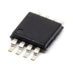
| 描述 | IC OPAMP VFB 560KHZ RRO 8MSOP精密放大器 Lo Pwr-Noise Lo Bias Crnt Prec Dual RRO |
| DevelopmentKit | EVAL-CN0240-SDPZ |
| 产品分类 | Linear - Amplifiers - Instrumentation, OP Amps, Buffer Amps集成电路 - IC |
| 品牌 | Analog Devices Inc |
| 产品手册 | |
| 产品图片 |
|
| rohs | 符合RoHS无铅 / 符合限制有害物质指令(RoHS)规范要求 |
| 产品系列 | 放大器 IC,精密放大器,Analog Devices AD8622ARMZ- |
| 数据手册 | |
| 产品型号 | AD8622ARMZ |
| 产品培训模块 | http://www.digikey.cn/PTM/IndividualPTM.page?site=cn&lang=zhs&ptm=30008http://www.digikey.cn/PTM/IndividualPTM.page?site=cn&lang=zhs&ptm=26202 |
| 产品目录页面 | |
| 产品种类 | 精密放大器 |
| 供应商器件封装 | 8-MSOP |
| 共模抑制比—最小值 | 135 dB |
| 关闭 | No |
| 包装 | 管件 |
| 压摆率 | 0.48 V/µs |
| 双重电源电压 | +/- 3 V, +/- 5 V, +/- 9 V, +/- 12 V |
| 可用增益调整 | 137 dB |
| 商标 | Analog Devices |
| 增益带宽生成 | 560 kHz |
| 增益带宽积 | 560kHz |
| 安装类型 | 表面贴装 |
| 安装风格 | SMD/SMT |
| 封装 | Tube |
| 封装/外壳 | 8-TSSOP,8-MSOP(0.118",3.00mm 宽) |
| 封装/箱体 | MSOP-8 |
| 工作温度 | -40°C ~ 125°C |
| 工作电源电压 | 2.5 V to 15 V |
| 工厂包装数量 | 50 |
| 放大器类型 | 电压反馈 |
| 最大双重电源电压 | +/- 15 V |
| 最大工作温度 | + 125 C |
| 最小双重电源电压 | +/- 2.5 V |
| 最小工作温度 | - 40 C |
| 标准包装 | 50 |
| 电压-电源,单/双 (±) | ±2.5 V ~ 15 V |
| 电压-输入失调 | 10µV |
| 电压增益dB | 137 dB |
| 电流-电源 | 215µA |
| 电流-输入偏置 | 45pA |
| 电流-输出/通道 | 40mA |
| 电源电压-最大 | 15 V |
| 电源电压-最小 | 2.5 V |
| 电源电流 | 215 uA |
| 电源类型 | Dual |
| 电路数 | 2 |
| 系列 | AD8622 |
| 视频文件 | http://www.digikey.cn/classic/video.aspx?PlayerID=1364138032001&width=640&height=505&videoID=2245193153001http://www.digikey.cn/classic/video.aspx?PlayerID=1364138032001&width=640&height=505&videoID=2245193159001 |
| 设计资源 | |
| 转换速度 | 0.48 V/us |
| 输入偏压电流—最大 | 500 pA |
| 输入电压范围—最大 | 13.8 V |
| 输入补偿电压 | 10 uV |
| 输出类型 | 满摆幅 |
| 通道数量 | 2 Channel |


- 商务部:美国ITC正式对集成电路等产品启动337调查
- 曝三星4nm工艺存在良率问题 高通将骁龙8 Gen1或转产台积电
- 太阳诱电将投资9.5亿元在常州建新厂生产MLCC 预计2023年完工
- 英特尔发布欧洲新工厂建设计划 深化IDM 2.0 战略
- 台积电先进制程称霸业界 有大客户加持明年业绩稳了
- 达到5530亿美元!SIA预计今年全球半导体销售额将创下新高
- 英特尔拟将自动驾驶子公司Mobileye上市 估值或超500亿美元
- 三星加码芯片和SET,合并消费电子和移动部门,撤换高东真等 CEO
- 三星电子宣布重大人事变动 还合并消费电子和移动部门
- 海关总署:前11个月进口集成电路产品价值2.52万亿元 增长14.8%


PDF Datasheet 数据手册内容提取
Low Power, Precision Rail-to-Rail Output Op Amp Data Sheet AD8622/AD8624 FEATURES PIN CONFIGURATIONS Very low offset voltage OUT A 1 8 V+ 125 μV maximum –IN A 2 AD8622 7 OUT B SInuppuptl yb icausr cruenrrte: n2t1:5 2 μ00A /paAm mp atyxpimicuaml +INV A– 34 (NToOt Pto V SIEcWale) 65 –+IINN BB 07527-001 Low input offset voltage drift: 1.2 μV/°C maximum Figure 1. 8-Lead Narrow-Body SOIC Very low voltage noise: 11 nV/√Hz Operating temperature: −40°C to +125°C OUT A 1 8 V+ AD8622 Rail-to-rail output swing –IN A 2 7 OUT B TOP VIEW U±2n.i5ty V g taoi n± 1st5a Vb loep eration +INV A– 34 (Not to Scale) 65 –+IINN BB 07527-002 Figure 2. 8-Lead MSOP APPLICATIONS Portable precision instrumentation OUT A 1 14 OUTD Laser diode control loops –IN A 2 13 –IND Strain gage amplifiers +IN A 3 AD8624 12 +IND TOP VIEW Medical instrumentation V+ 4 (Not to Scale) 11 V– Thermocouple amplifiers +IN B 5 10 +INC –IN B 6 9 –INC GENERAL DESCRIPTION OUT B 7 8 OUTC07527-067 Figure 3. 14-Lead TSSOP The AD8622/AD8624 are dual and quad precision rail-to-rail A D output operational amplifiers with low supply currents of only T T C U U C N O O N 350 μA/amplifier maximum over temperature and supply voltages. 61 51 41 31 The AD8622/AD8624 also has an input bias current cancellation circuitry that provides a very low input bias current over the full –IN A 1 12 –IN D operating temperature. +IN A 2 AD8624 11 +IN D V+ 3 TOP VIEW 10 V– (Not to Scale) With a typical offset voltage of only 10 μV, offset drift of 0.5 μV/°C, +IN B 4 9 +IN C and noise of only 0.2 μV p-p (0.1 Hz to 10 Hz), they are perfectly 5 6 78 suited for applications where large error sources cannot be B B C C N T T N tolerated. Many systems can take advantage of the low noise, –I UO UO –I dc precision, and rail-to-rail output swing provided by the NOTES AdyDn8a6m2i2c/ AraDng8e6 2fo4r t loo wm apxoiwmeirz eo ptheer astiigonna. lT-thoe-n AoDis8e 6r2a2ti/oA aDn8d6 24 12 .. INPTAC ID S= BRNEEO CC COOOMNNMNNEEENCCDTTEE.DD TTOHA VT– .THE EXPOSED 07527-068 Figure 4. 16-Lead LFCSP are specified for the extended industrial temperature range of −40°C to +125°C. The AD8622 is available in lead-free 8-lead SOIC and MSOP packages, while the AD8624 is available in Table 1. Low Power Op Amps lead-free 14-lead TSSOP and 16-lead LFCSP packages. Supply 40 V 36 V 12 V to 18 V 6 V Single OP97 OP777 AD8663 OP1177 Dual OP297 OP727 AD8667 ADA4692-2 OP2177 Quad OP497 OP747 AD8669 ADA4692-4 OP4177 Rev. D Document Feedback Information furnished by Analog Devices is believed to be accurate and reliable. However, no responsibility is assumed by Analog Devices for its use, nor for any infringements of patents or other One Technology Way, P.O. Box 9106, Norwood, MA 02062-9106, U.S.A. rights of third parties that may result from its use. Specifications subject to change without notice. No license is granted by implication or otherwise under any patent or patent rights of Analog Devices. Tel: 781.329.4700 ©2009–2013 Analog Devices, Inc. All rights reserved. Trademarks and registered trademarks are the property of their respective owners. Technical Support www.analog.com
AD8622/AD8624 Data Sheet TABLE OF CONTENTS Features .............................................................................................. 1 ESD Caution...................................................................................5 Applications ....................................................................................... 1 Typical Performance Characteristics ..............................................6 General Description ......................................................................... 1 Applications Information .............................................................. 15 Pin Configurations ........................................................................... 1 Input Protection ......................................................................... 15 Revision History ............................................................................... 2 Phase Reversal ............................................................................ 15 Specifications ..................................................................................... 3 Micropower Instrumentation Amplifier ................................. 15 Electrical Characteristics—±2.5 V Operation .......................... 3 Hall Sensor Signal Conditioning .............................................. 16 Electrical Characteristics—±15 V Operation ........................... 4 Simplified Schematic ...................................................................... 17 Absolute Maximum Ratings ............................................................ 5 Outline Dimensions ....................................................................... 18 Thermal Resistance ...................................................................... 5 Ordering Guide .......................................................................... 19 REVISION HISTORY 12/13—Rev. C to Rev. D Change to Figure 58 ....................................................................... 17 Updated Outline Dimensions ....................................................... 19 6/11—Rev. B to Rev. C Changes to Figure 13 ........................................................................ 7 2/10—Rev. A to Rev. B Changed 16-Lead to 14-Lead in Figure 62 Caption ................... 19 1/10—Rev. 0 to Rev. A Added 14-Lead TSSOP ...................................................... Universal Added 16-Lead LFCSP ....................................................... Universal Added Figure 3 and Figure 4; Renumbered Sequentially ........... 1 Changes to Table 5 ............................................................................ 5 Changes to Figure 10 to Figure 16 .................................................. 6 Changes to Figure 26 ........................................................................ 9 Changes to Figure 29 ...................................................................... 10 Updated Outline Dimensions ....................................................... 18 Changes to Ordering Guide .......................................................... 19 7/09—Revision 0: Initial Version Rev. D | Page 2 of 20
Data Sheet AD8622/AD8624 SPECIFICATIONS ELECTRICAL CHARACTERISTICS—±2.5 V OPERATION V = ±2.5 V, V = 0 V, T = 25°C, unless otherwise specified. SY CM A Table 2. Parameter Symbol Conditions Min Typ Max Unit INPUT CHARACTERISTICS Offset Voltage V 10 125 μV OS −40°C ≤ T ≤ +125°C 230 μV A Offset Voltage Drift ΔV /ΔT −40°C ≤ T ≤ +125°C 0.5 1.2 µV/°C OS A Input Bias Current I 30 200 pA B −40°C ≤ T ≤ +125°C 400 pA A Input Offset Current I 25 200 pA OS −40°C ≤ T ≤ +125°C 300 pA A Input Voltage Range −40°C ≤ T ≤ +125°C −1.3 +1.3 V A Common-Mode Rejection Ratio CMRR V = −1.3 V to +1.3 V 110 120 dB CM −40°C ≤ T ≤ +125°C 107 dB A Open-Loop Gain A R = 10 kΩ, V = −2.0 V to +2.0 V 118 135 dB VO L O −40°C ≤ T ≤ +125°C 109 dB A Input Resistance, Differential Mode R 1 GΩ INDM Input Resistance, Common Mode R 1 TΩ INCM Input Capacitance, Differential Mode C 5.5 pF INDM Input Capacitance, Common Mode C 3 pF INCM OUTPUT CHARACTERISTICS Output Voltage High V R = 100 kΩ to ground 2.45 2.49 V OH L −40°C ≤ T ≤ +125°C 2.41 V A R = 10 kΩ to ground 2.40 2.45 V L −40°C ≤ T ≤ +125°C 2.36 V A Output Voltage Low V R = 100 kΩ to ground −2.49 −2.45 V OL L −40°C ≤ T ≤ +125°C −2.41 V A R = 10 kΩ to ground −2.45 −2.40 V L −40°C ≤ T ≤ +125°C −2.36 V A Short-Circuit Current I ±30 mA SC Closed-Loop Output Impedance Z f = 1 kHz, A = 1 2 Ω OUT V POWER SUPPLY Power Supply Rejection Ratio PSRR V = ±2.0 V to ±18.0 V 125 145 dB S −40°C ≤ T ≤ +125°C 120 dB A Supply Current/Amplifier I I = 0 mA 175 225 μA SY O −40°C ≤ T ≤ +125°C 310 μA A DYNAMIC PERFORMANCE Slew Rate SR R = 10 kΩ, C = 100 pF A = 1 0.28 V/μs L L V Gain Bandwidth Product GBP R = 10 kΩ, C = 20 pF, A = 1 540 kHz L L V Phase Margin Φ R = 10 kΩ, C = 20 pF, A = 1 74 Degrees M L L V NOISE PERFORMANCE Voltage Noise e p-p f = 0.1 Hz to 10 Hz 0.2 μV p-p n Voltage Noise Density e f = 1 kHz 12 nV/√Hz n Uncorrelated Current Noise Density i f = 1 kHz 0.15 pA/√Hz n_uncorr Correlated Current Noise Density i f = 1 kHz 0.07 pA/√Hz n_corr Rev. D | Page 3 of 20
AD8622/AD8624 Data Sheet ELECTRICAL CHARACTERISTICS—±15 V OPERATION V = ±15 V, V = 0 V, T = 25°C, unless otherwise specified. SY CM A Table 3. Parameter Symbol Conditions Min Typ Max Unit INPUT CHARACTERISTICS Offset Voltage V 10 125 μV OS −40°C ≤ T ≤ +125°C 230 μV A Offset Voltage Drift ΔV /ΔT −40°C ≤ T ≤ +125°C 0.5 1.2 μV/°C OS A Input Bias Current I 45 200 pA B −40°C ≤ T ≤ +125°C 500 pA A Input Offset Current I 35 200 pA OS −40°C ≤ T ≤ +125°C 500 pA A Input Voltage Range −13.8 +13.8 V Common-Mode Rejection Ratio CMRR V = −13.8 V to +13.8 V 125 135 dB CM −40°C ≤ T ≤ +125°C 112 dB A Open-Loop Gain A R = 10 kΩ, V = −13.5 V to +13.5 V 125 137 dB VO L O −40°C ≤ T ≤ +125°C 120 dB A Input Resistance, Differential Mode R 1 GΩ INDM Input Resistance, Common Mode R 1 TΩ INCM Input Capacitance, Differential Mode C 5.5 pF INDM Input Capacitance, Common Mode C 3 pF INCM OUTPUT CHARACTERISTICS Output Voltage High V R = 100 kΩ to ground 14.94 14.97 V OH L −40°C ≤ T ≤ +125°C 14.84 V A R = 10 kΩ to ground 14.86 14.89 V L −40°C ≤ T ≤ +125°C 14.75 V A Output Voltage Low V R = 100 kΩ to ground −14.97 −14.94 V OL L −40°C ≤ T ≤ +125°C −14.92 V A R = 10 kΩ to ground −14.89 −14.90 V L −40°C ≤ T ≤ +125°C −14.80 V A Short-Circuit Current I ±40 mA SC Closed-Loop Output Impedance Z f = 1 kHz, A = 1 1.5 Ω OUT V POWER SUPPLY Power Supply Rejection Ratio PSRR V = ±2.0 V to ±18.0 V 125 145 dB S −40°C ≤ T ≤ +125°C 120 dB A Supply Current/Amplifier I I = 0 mA 215 250 μA SY O −40°C ≤ T ≤ +125°C 350 μA A DYNAMIC PERFORMANCE Slew Rate SR R = 10 kΩ, C = 100 pF, A = 1 0.48 V/μs L L V Gain Bandwidth Product GBP R = 10 kΩ, C = 20 pF, A = 1 560 kHz L L V Phase Margin Φ R = 10 kΩ, C = 20 pF, A = 1 75 Degrees M L L V NOISE PERFORMANCE Voltage Noise e p-p f = 0.1 Hz to 10 Hz 0.2 μV p-p n Voltage Noise Density e f = 1 kHz 11 nV/√Hz n Uncorrelated Current Noise Density i f = 1 kHz 0.15 pA/√Hz n_uncorr Correlated Current Noise Density i f = 1 kHz 0.06 pA/√Hz n_corr Rev. D | Page 4 of 20
Data Sheet AD8622/AD8624 ABSOLUTE MAXIMUM RATINGS Table 2. THERMAL RESISTANCE Parameter Rating Supply Voltage ±18 V θJA is specified for the worst-case conditions, that is, a device Input Voltage ±V soldered in a circuit board for surface-mount packages. This SY Input Current1 ±10 mA was measured using a standard 4-layer board. Differential Input Voltage2 ±10 V Table 3. Thermal Resistance Output Short-Circuit Duration to GND Indefinite Package Type θ θ Unit Storage Temperature Range −65°C to +150°C JA JC 8-Lead SOIC_N (R-8) 120 45 °C/W Operating Temperature Range −40°C to +125°C 8-Lead MSOP (RM-8) 142 45 °C/W Junction Temperature Range −65°C to +150°C 14-Lead TSSOP (RU-14) 112 35 °C/W Lead Temperature (Soldering, 60 sec) 300°C 16-Lead LFCSP (CP-16-17) 55 14 °C/W 1 The input pins have clamp diodes to the power supply pins. The input current should be limited to 10 mA or less whenever input signals exceed the power supply rail by 0.5 V. ESD CAUTION 2 Differential input voltage is limited to 10 V or the supply voltage, whichever is less. Stresses above those listed under Absolute Maximum Ratings may cause permanent damage to the device. This is a stress rating only; functional operation of the device at these or any other conditions above those indicated in the operational section of this specification is not implied. Exposure to absolute maximum rating conditions for extended periods may affect device reliability. Rev. D | Page 5 of 20
AD8622/AD8624 Data Sheet TYPICAL PERFORMANCE CHARACTERISTICS T = 25°C, unless otherwise noted. A 60 60 VSY = ±2.5V VSY = ±15V VCM = 0V VCM = 0V 50 50 S S R R FIE 40 FIE 40 LI LI P P M M F A 30 F A 30 O O R R E E MB 20 MB 20 U U N N 10 10 –0100 –80 –60 –40 –20 VO0S (µV2)0 40 60 80 100 07527-065 –0100 –80 –60 –40 –20 VO0S (µV2)0 40 60 80 100 07527-063 Figure 5. Input Offset Voltage Distribution Figure 8. Input Offset Voltage Distribution 60 60 VSY = ±2.5V VSY = ±15V –40°C ≤ TA ≤ +125°C –40°C ≤ TA ≤ +125°C 50 50 S S R R FIE 40 FIE 40 LI LI P P M M F A 30 F A 30 O O R R E E MB 20 MB 20 U U N N 10 10 00 0.2 0.4 TCVOS0 .(6µV/°C) 0.8 1.0 1.2 07527-066 00 0.2 0.4 TCVOS0 .(6µV/°C) 0.8 1.0 1.207527-064 Figure 6. Input Offset Voltage Drift Distribution Figure 9. Input Offset Voltage Drift Distribution 50 50 VSY = ±2.5V VSY = ±15V 40 40 –40°C 30 30 20 20 –40°C 10 10 V) V) µ +25°C µ (S 0 (S 0 O O V V +25°C –10 –10 +85°C +85°C –20 –20 +125°C +125°C –30 –30 –40 –40 –50–2.5 –1.5 –0.5VCM (V) 0.5 1.5 2.5 07527-007 –50–15 –10 –5 VCM0 (V) 5 10 +1507527-004 Figure 7. Input Offset Voltage vs. Common-Mode Voltage Figure 10. Input Offset Voltage vs. Common-Mode Voltage Rev. D | Page 6 of 20
Data Sheet AD8622/AD8624 0 10 VSY = ±2.5V VSY = ±15V IB+ –10 0 IB+ IB– –20 –10 (pA)B–30 IB– I (pA)B–20 I –40 –30 –50 –40 –60–50 –25 0 TEMP25ERATUR5E0(°C) 75 100 125 07527-008 –50–50 –25 0 TEMP25ERATUR5E0(°C) 75 100 125 07527-011 Figure 11. Input Bias Current vs. Temperature Figure 14. Input Bias Current vs. Temperature 50 60 VSY = ±2.5V VSY = ±15V 25 40 0 20 –25 A) A) I (pB–50 I (pB 0 –75 –20 –100 –40 –125 –150–2.5 –1.5 –0.5VCM (V) 0.5 1.5 2.5 07527-012 –60–15 –10 –5 VCM0 (V) 5 10 15 07527-009 Figure 12. Input Bias Current vs. Common-Mode Voltage Figure 15. Input Bias Current vs. Common-Mode Voltage 10 100 VSY = ±2.5V VSY = ±15V OUTPUT VOLTAGE TO SUPPLY RAIL (V)0.00.111 VCC – VOH VOL – VEE OUTPUT VOLTAGE TO SUPPLY RAIL (V)0.010.0111 VCCV O–L V –O VHEE 0.0010.01 0.1 LOAD CUR1RENT (mA) 10 100 07527-013 0.0010.01 0.1 LOAD CUR1RENT (mA) 10 100 07527-010 Figure 13. Output Voltage to Supply Rail vs. Load Current Figure 16. Output Voltage to Supply Rail vs. Load Current Rev. D | Page 7 of 20
AD8622/AD8624 Data Sheet 0.06 0.16 VSY = ±2.5V VSY = ±15V L (V)0.05 RL = 10kΩ L (V)0.14 RL = 10kΩ AI AI Y R VCC – VOH Y R0.12 VCC – VOH L L P0.04 P UP UP0.10 S S O O T0.03 T0.08 E E G G A A T T0.06 VOL0.02 VOL VOL – VEE UT VOL – VEE UT 0.04 P P T0.01 T OU OU0.02 0–50 –25 0 TEMP25ERATUR5E0 (°C) 75 100 125 07527-017 0–50 –25 0 TEMP25ERATUR5E0 (°C) 75 100 125 07527-014 Figure 17. Output Voltage to Supply Rail vs. Temperature Figure 20. Output Voltage to Supply Rail vs. Temperature 0.35 0.35 0.30 +125°C 0.30 0.25 +85°C 0.25 0.20 VSY = ±15V A) +25°C A) m m (SY0.15 –40°C (SY0.20 I I VSY = ±2.5V 0.10 0.15 0.05 0.10 0 –0.050 2 4 6 V8SY (±V10) 12 14 16 18 07527-044 0.05–50 –25 0 TEMP25ERATUR5E0 (°C) 75 100 125 07527-045 Figure 18. Supply Current vs. Supply Voltage Figure 21. Supply Current vs. Temperature 100 100 100 100 VSY = ±2.5V VSY = ±15V RL = 10kΩ RL = 10kΩ 80 PHASE 80 80 PHASE 80 60 60 60 60 s) s) e e GAIN (dB) 4200 GAIN 4200 ASE (Degre GAIN (dB) 4200 GAIN 4200 ASE (Degre H H P P 0 0 0 0 –20 –20 –20 –20 –401k 10k FREQU1E0N0kCY (Hz) 1M 10M–40 07527-018 –401k 10k FREQU1E0N0kCY (Hz) 1M 10M–40 07527-015 Figure 19. Open-Loop Gain and Phase vs. Frequency Figure 22. Open-Loop Gain and Phase vs. Frequency Rev. D | Page 8 of 20
Data Sheet AD8622/AD8624 60 60 VSY = ±2.5V VSY = ±15V 50 RL = 10kΩ 50 RL = 10kΩ AV = 100 AV = 100 40 40 30 30 AV = 10 AV = 10 B) 20 B) 20 d d N ( 10 N ( 10 AI AV = 1 AI AV = 1 G 0 G 0 –10 –10 –20 –20 –30 –30 –40100 1k F1R0EkQUENCY1 (0H0zk) 1M 10M 07527-019 –40100 1k F1R0EkQUENCY1 (0H0zk) 1M 10M 07527-016 Figure 23. Closed-Loop Gain vs. Frequency Figure 26. Closed-Loop Gain vs. Frequency 10k 10k VSY = ±2.5V VSY = ±15V 1k AV = 100 1k AV = 100 AV = 10 AV = 10 Ω)100 AV = 1 Ω)100 AV = 1 (UT (UT O O Z Z 10 10 1 1 0.1100 1k FREQU1E0NkCY (Hz) 100k 1M 07527-023 0.1100 1k FREQU1E0NkCY (Hz) 100k 1M 07527-020 Figure 24. Output Impedance vs. Frequency Figure 27. Output Impedance vs. Frequency 140 140 VSY = ±2.5V VSY = ±15V 120 120 100 100 B) 80 B) 80 d d R ( R ( R R M 60 M 60 C C 40 40 20 20 010 100 FR1kEQUENCY 1(H0kz) 100k 1M07527-021 010 100 FR1kEQUENCY 1(H0kz) 100k 1M07527-024 Figure 25. CMRR vs. Frequency Figure 28. CMRR vs. Frequency Rev. D | Page 9 of 20
AD8622/AD8624 Data Sheet 120 120 VSY = ±2.5V VSY = ±15V 100 100 PSRR+ PSRR+ 80 80 B) B) d d R ( 60 R ( 60 R R S S P PSRR– P PSRR– 40 40 20 20 010 100 FR1kEQUENCY 1(H0kz) 100k 1M 07527-025 010 100 FR1kEQUENCY 1(H0kz) 100k 1M 07527-022 Figure 29. PSRR vs. Frequency Figure 32. PSRR vs. Frequency 50 50 VSY = ±2.5V VSY = ±15V 45 AV = 1 45 AV = 1 RL = 10kΩ RL = 10kΩ 40 40 35 35 %) OS– %) OT (30 OT (30 OS– HO25 OS+ HO25 OS+ S S R R E20 E20 V V O O 15 15 10 10 5 5 00.01 0.1 CAPACITA1NCE (nF) 10 100 07527-029 00.01 0.1 CAPACITA1NCE (nF) 10 100 07527-026 Figure 30. Small-Signal Overshoot vs. Load Capacitance Figure 33. Small-Signal Overshoot vs. Load Capacitance VARCSVLLY === = 111 00±k02Ωp.5FV VARCSVLLY === = 111 00±k01Ωp5VF V) DI V) V/ DI E (500m GE (5V/ G A A T LT OL O V V TIME (40µs/DIV) 07527-030 TIME (40µs/DIV) 07527-027 Figure 31. Large-Signal Transient Response Figure 34. Large-Signal Transient Response Rev. D | Page 10 of 20
Data Sheet AD8622/AD8624 VSY = ±2.5V VSY = ±15V AV = 1 AV = 1 RL = 10kΩ RL = 10kΩ CL = 100pF CL = 100pF V) V) DI DI V/ V/ m m 0 0 5 5 E ( E ( G G A A T T L L O O V V TIME (10µs/DIV) 07527-031 TIME (10µs/DIV) 07527-028 Figure 35. Small-Signal Transient Response Figure 38. Small-Signal Transient Response 0.4 0.4 VSY = ±2.5V VSY = ±15V 0.2 AV = –100 0.2 AV = –100 INPUT RL = 10kΩ INPUT RL = 10kΩ 0 0 NPUT VOLTAGE (V) OUTPUT 0 UTPUT VOLTAGE (V) NPUT VOLTAGE (V) OUTPUT 0 UTPUT VOLTAGE (V) I O I O –1 –10 –2 –20 TIME (20µs/DIV) –3 07527-035 TIME (20µs/DIV) 07527-032 Figure 36. Negative Overload Recovery Figure 39. Negative Overload Recovery 0.2 0.2 INPUT INPUT 0 0 –0.2 –0.2 NPUT VOLTAGE (V) 23 UTPUT VOLTAGE (V) NPUT VOLTAGE (V) 1200 UTPUT VOLTAGE (V) I OUTPUT O I OUTPUT O 1 0 AVSVY = = – ±120.05V 0 VASVY = = – ±11050V –10 RL = 10kΩ TIME (20µs/DIV) –1 07527-036 RL = 10kΩ TIME (20µs/DIV) –20 07527-033 Figure 37. Positive Overload Recovery Figure 40. Positive Overload Recovery Rev. D | Page 11 of 20
AD8622/AD8624 Data Sheet 12 12 VSY = ±15V VSY = ±15V AV = –1 AV = +1 10 10 V) 8 V) 8 P ( P ( 0.1% E E T 0.1% 0.01% T 0.01% T S 6 T S 6 U U P P T T U U O 4 O 4 2 2 00 5 10 SETT1L5ING TIM20E (µs) 25 30 35 07527-034 00 5 10 SETT1L5ING TIM20E (µs) 25 30 35 07527-037 Figure 41. Output Step vs. Settling Time Figure 44. Output Step vs. Settling Time 100 100 VSY = ±2.5V VSY = ±15V Hz) Hz) VOLTAGE NOISE DENSITY (nV/ 10 VOLTAGE NOISE DENSITY (nV 10 11 10FREQUENCY (Hz)100 1k 07527-042 11 10FREQUENCY (Hz)100 1k 07527-039 Figure 42. Voltage Noise Density vs. Frequency Figure 45. Voltage Noise Density vs. Frequency 1 1 RS1 VSY = ±2.5V RS1 VSY = ±15V Hz) Hz) A/ RS2 A/ RS2 NSITY (p URNS1C =O 0RΩRELATED NSITY (p URNS1C =O 0RΩRELATED OISE DE0.1 CROS1R =R RELS2ATED OISE DE0.1 CROS1R =R RELS2ATED N N NT NT CURRE CURRE 0.011 10FREQUENCY (Hz)100 1k 07527-057 0.011 10FREQUENCY (Hz)100 1k 07527-056 Figure 43. Current Noise Density vs. Frequency Figure 46. Current Noise Density vs. Frequency Rev. D | Page 12 of 20
Data Sheet AD8622/AD8624 VSY = ±2.5V VSY = ±15V V) V) DI DI V/ V/ n n 0 0 5 5 E ( E ( G G A A T T L L O O V V E E S S OI OI N N T T U U P P N N I I TIME (1s/DIV) 07527-043 TIME (1s/DIV) 07527-040 Figure 47. 0.1 Hz to 10 Hz Noise Figure 49. 0.1 Hz to 10 Hz Noise 1 1 VSY = ±2.5V VSY = ±15V f = 1kHz f = 1kHz RL = 10kΩ RL = 10kΩ 0.1 0.1 %) %) N ( N ( + 0.01 + 0.01 D D H H T T 0.001 0.001 0.00001.001 0.01 AMPLITU0D.1E (V rms) 1 10 07527-049 0.00001.001 0.01 AMPLITU0D.1E (V rms) 1 10 07527-046 Figure 48. THD + Noise vs. Amplitude Figure 50. THD + Noise vs. Amplitude Rev. D | Page 13 of 20
AD8622/AD8624 Data Sheet 0.1 0.1 RVVSILNY = == 1 30±0k20Ω.m5VV rms RVVSILNY = == 1 30±0k10Ω5mVV rms 0.01 0.01 %) %) N ( N ( + + D D H H T T 0.001 0.001 0.000110 100 FREQUE1NkCY (Hz) 10k 100k 07527-051 0.000110 100 FREQUE1NkCY (Hz) 10k 100k 07527-050 Figure 51. THD + Noise vs. Frequency Figure 53. THD + Noise vs. Frequency 0 100kΩ –20 1kΩ B) N (d –40 RL O TI A –60 R PA E L S –80 E N N A–100 H C –120 VSY = ±2.5VTO ±15V RL = 10kΩ AV = –100 –14010 100 FREQUE1NkCY (Hz) 10k 100k 07527-048 Figure 52. Channel Separation vs. Frequency Rev. D | Page 14 of 20
Data Sheet AD8622/AD8624 APPLICATIONS INFORMATION INPUT PROTECTION VIN VSY = ±15V The maximum differential input voltage that can be applied to the AD8622/AD8624 is determined by the internal diodes VOUT connected across its inputs and series resistors at each input. V) These internal diodes and series resistors limit the maximum V/DI 5 differential input voltage to ±10 V and are needed to prevent base- E ( G emitter junction breakdown from occurring in the input stage of A T L the AD8622/AD8624 when very large differential voltages are O V applied. In addition, the internal resistors limit the currents that flow through the diodes. However, in applications where large differential voltages can be inadvertently applied to the device, lcaarsgee, ecxutrerrennatls rmesaiyst sotrisll mflouwst tbher opulagche dth aets beo dtiho idnepsu. Itns osfu tchhe a o p TIME (200µs/DIV) 07527-053 Figure 55. No Phase Reversal amp to limit the input currents to ±10 mA (see Figure 54). MICROPOWER INSTRUMENTATION AMPLIFIER The AD8622 is a dual, high precision, rail-to-rail output op amp R1 2 500Ω operating at just 215 μA quiescent current per amplifier. Its 1 ultralow offset, offset drift, and voltage noise, combined with its AD862x very low bias current and high common-mode rejection ratio R2 3 500Ω (CMRR), are ideally suited for high accuracy and micropower 07527-055 iFnigsturruem 5e6n sthaotiwons tahme pclliafsiesirc. 2-op-amp instrumentation amplifier Figure 54. Input Protection with four resistors using the AD8622. The key to high CMRR PHASE REVERSAL for this instrumentation amplifier are resistors that are well An undesired phenomenon, phase reversal (also known as matched from both the resistive ratio and the relative drift. For phase inversion) occurs in many op amps when one or both of true difference amplification, matching of the resistor ratio is the inputs are driven beyond the specified input voltage range very important, where R3/R4 = R1/R2. Assuming perfectly (IVR), in effect reversing the polarity of the output. In some matched resistors, the gain of the circuit is 1 + R2/R1, which is cases, phase reversal can induce lockups and even cause approximately 100. Tighter matching of two op amps in one equipment damage as well as self destruction. package, like the AD8622, offers a significant boost in performance over the classical 3-op-amp configuration. Overall, the circuit The AD8622/AD8624 amplifiers have been carefully designed to only requires about 430 μA of supply current. prevent output phase reversal when both inputs are maintained R3 within the specified input voltage range. In addition, even if one 10.1kΩ R2 or both inputs exceed the input voltage range but remain within 1MΩ +15V the supply rails, the output still does not phase reverse. Figure 55 R4 1MΩ +15V shows the input/output waveforms of the AD8622/AD8624 – R1 1/2 10.1kΩ configured as a unity-gain buffer with a supply voltage of ±15 V. AD8622 – 1/2 V1 + AD8622 VO –15V V2 + NOTES –15V 1. VO = 100(V2 – V1) 423... TTUYYSPPEII CCMAAALLT::C 0–H.10E41D.m9 7RVVE <<S |IVVSO2T O–< R V+S11.4| .<9 71V49.7mV 07527-054 Figure 56. Micropower Instrumentation Amplifier Rev. D | Page 15 of 20
AD8622/AD8624 Data Sheet HALL SENSOR SIGNAL CONDITIONING magnetic field. Using the 4.12k:98.8k resistive divider, the bias voltage of the Hall element is reduced to 100 mV, leading to only The AD8622/AD8624 is also highly suitable for high accuracy, 250 µA of power consumption. The 3-op-amp in-amp low power signal conditioning circuits. One such use is in Hall configuration of the AD8622/AD8624 then increases the sensor signal conditioning (see Figure 57). The magnetic sensitivity to 55 mV/mT. The key to high CMRR for this in-amp sensitivity of a Hall element is proportional to the bias voltage configuration are resistors that are well matched (where R1/R2 applied across it. With 1 V bias voltage, the Hall element = R3/R4) from both the resistive ratio and relative drift. The consumes about 2.5 mA of supply current and has a sensitivity resistors are important in determining the performance over of 5.5 mV/mT typical. To reduce power consumption, bias manufacturing tolerances, time and temperature. At least 1% or voltage must be reduced, but at the risk of lower sensitivity. The better resistors are recommended. Using the AD8622/AD8624 to only way to achieve higher sensitivity is by introducing a gain amplify the sensor signal can reduce power while also achieving using a precision micropower amplifier. The AD8622/AD8624, higher sensitivity. The total current consumed is just 1.2 mA, with all its features, is well suited to amplify the sensitivity of the resulting in 21× improvement in sensitivity/power. Hall element. The ADR121 is a precision micropower 2.5 V voltage reference. A precision voltage reference is required to hold a constant current so that the Hall voltage only depends on the intensity of the VSY VSY + C1 R2 1µFTO 10µF HALL AD862x 9.9kΩ ELEMENT – R5 R1 VSY ADR121 – 2.5V 9.9kΩ 9.9kΩ – R8 VSY 0.1CµF2 TO0 1.10CµµFF3 + 4.12kRΩ9 A+D862x 40×04Ω R2070Ω 9.R9k6Ω 9.R9k3Ω A+D862x VOUT = 2.5V + 55mmTV× MAGNETIC FIELD (mT) 98.8kΩ VSY – – AD862x R4 9.9kΩ + N12..O UFTOSEERS MINAFTOCRHMEADT RIOENS IOSNTO CR1S, CF2O,RA NIND- ACM3,P R.EFERTOADR121 DATA SHEET. 07527-052 Figure 57. Hall Sensor Signal Conditioning Rev. D | Page 16 of 20
Data Sheet AD8622/AD8624 SIMPLIFIED SCHEMATIC V+ R3 R2 R1 Q10 Q11 C1 Q3 VB1 VB2 Q6 Q4 INPUT BIAS Q5 CANCELLATION 500Ω CIRCUITRY Q8 OUT x +IN x Q1 Q2 D1 D2 500Ω –IN x Q7 Q12 Q9 V– D3 VBIAS 07527-062 Figure 58. Simplified Schematic Rev. D | Page 17 of 20
AD8622/AD8624 Data Sheet OUTLINE DIMENSIONS 3.20 3.00 2.80 8 5 5.15 3.20 4.90 3.00 4.65 2.80 1 4 PIN1 IDENTIFIER 0.65BSC 0.95 15°MAX 0.85 1.10MAX 0.75 0.80 0.15 0.40 6° 0.23 0.55 CO0P.0L5ANARITY 0.25 0° 0.09 0.40 0.10 COMPLIANTTOJEDECSTANDARDSMO-187-AA 100709-B Figure 59. 8-Lead Mini Small Outline Package [MSOP] (RM-8) Dimensions shown in millimeters 5.00(0.1968) 4.80(0.1890) 8 5 4.00 (0.1574) 6.20 (0.2441) 3.80 (0.1497) 1 4 5.80 (0.2284) 1.27 (0.0500) 0.50 (0.0196) BSC 1.75 (0.0688) 0.25 (0.0099) 45° 0.25 (0.0098) 1.35 (0.0532) 8° 0.10 (0.0040) 0° COPLANARITY 0.51 (0.0201) 0.10 SEATING 0.31 (0.0122) 0.25 (0.0098) 10..2470 ((00..00510507)) PLANE 0.17 (0.0067) COMPLIANTTO JEDEC STANDARDS MS-012-AA RC(INEOFNPEATRRREOENNLCLTEIHN EOGSN EDLSIYM)AEANNRDSEI AORRNOESU NANORDEET DAIN-PO MPFRIFLO LMPIIMRLELIATIMTEEER TFSEO; RIRN ECUQHSU EDI VIINMA LEDENENSSTIIOGSN NFS.OR A012407- Figure 60. 8-Lead Standard Small Outline Package [SOIC_N] Narrow Body (R-8) Dimensions shown in millimeters and (inches) Rev. D | Page 18 of 20
Data Sheet AD8622/AD8624 4.10 0.35 4.00 SQ 0.30 PIN 1 3.90 0.25 INDICATOR PIN 1 0.65 13 16 INDICATOR BSC 12 1 EXPOSED 2.70 PAD 2.60 SQ 2.50 4 9 0.45 8 5 0.20 MIN TOP VIEW 0.40 BOTTOM VIEW 0.35 0.80 FOR PROPER CONNECTION OF 0.75 THE EXPOSED PAD, REFER TO 0.70 0.05 MAX THE PIN CONFIGURATION AND 0.02 NOM SECTION OF THIS DATA SHEET. COPLANARITY SEATING 0.08 PLANE 0.20 REF COMPLIANTTOJEDEC STANDARDS MO-220-WGGC. 08-16-2010-C Figure 61. 16-Lead Lead Frame Chip Scale Package [LFCSP_WQ] 4 mm × 4mm Body, Very Very Thin Quad (CP-16-17) Dimensions shown in millimeters 5.10 5.00 4.90 14 8 4.50 4.40 6.40 BSC 4.30 1 7 PIN 1 0.65 BSC 1.05 1.00 1M.A20X 0.20 0.80 0.09 0.75 0.15 8° 0.60 0.05 0.30 SPELAATNIENG 0° 0.45 COPLANARITY 0.19 0.10 COMPLIANT TO JEDEC STANDARDS MO-153-AB-1 061908-A Figure 62. 14-Lead Thin Shrink Small Outline Package [TSSOP] (RU-14) Dimensions shown in millimeters ORDERING GUIDE Model1 Temperature Range Package Description Package Option Branding AD8622ARMZ −40°C to +125°C 8-Lead MSOP RM-8 A1P AD8622ARMZ-REEL −40°C to +125°C 8-Lead MSOP RM-8 A1P AD8622ARMZ-R7 −40°C to +125°C 8-Lead MSOP RM-8 A1P AD8622ARZ −40°C to +125°C 8-Lead SOIC_N R-8 AD8622ARZ-REEL −40°C to +125°C 8-Lead SOIC_N R-8 AD8622ARZ-REEL7 −40°C to +125°C 8-Lead SOIC_N R-8 AD8624ACPZ-R2 −40°C to +125°C 16-Lead LFCSP_WQ CP-16-17 AD8624ACPZ-R7 −40°C to +125°C 16-Lead LFCSP_WQ CP-16-17 AD8624ACPZ-RL −40°C to +125°C 16-Lead LFCSP_WQ CP-16-17 AD8624ARUZ −40°C to +125°C 14-Lead TSSOP RU-14 AD8624ARUZ-RL −40°C to +125°C 14-Lead TSSOP RU-14 1 Z = RoHS Compliant Part. Rev. D | Page 19 of 20
AD8622/AD8624 Data Sheet NOTES ©2009–2013 Analog Devices, Inc. All rights reserved. Trademarks and registered trademarks are the property of their respective owners. D07527-0-12/13(D) Rev. D | Page 20 of 20
Mouser Electronics Authorized Distributor Click to View Pricing, Inventory, Delivery & Lifecycle Information: A nalog Devices Inc.: AD8622ARMZ AD8622ARZ AD8624ACPZ-R2 AD8624ARUZ AD8622ARMZ-R7 AD8622ARMZ-REEL AD8622ARZ-REEL AD8622ARZ-REEL7 AD8624ACPZ-R7 AD8624ACPZ-RL AD8624ARUZ-RL