ICGOO在线商城 > 集成电路(IC) > 线性 - 放大器 - 仪表,运算放大器,缓冲器放大器 > AD8613AKSZ-R2
 Datasheet下载
- 型号: AD8613AKSZ-R2
- 制造商: Analog
- 库位|库存: xxxx|xxxx
- 要求:
| 数量阶梯 | 香港交货 | 国内含税 |
| +xxxx | $xxxx | ¥xxxx |
查看当月历史价格
查看今年历史价格
AD8613AKSZ-R2产品简介:
ICGOO电子元器件商城为您提供AD8613AKSZ-R2由Analog设计生产,在icgoo商城现货销售,并且可以通过原厂、代理商等渠道进行代购。 AD8613AKSZ-R2价格参考。AnalogAD8613AKSZ-R2封装/规格:线性 - 放大器 - 仪表,运算放大器,缓冲器放大器, General Purpose Amplifier 1 Circuit Rail-to-Rail SC-70-5。您可以下载AD8613AKSZ-R2参考资料、Datasheet数据手册功能说明书,资料中有AD8613AKSZ-R2 详细功能的应用电路图电压和使用方法及教程。
AD8613AKSZ-R2是Analog Devices Inc.生产的一款低功耗、单通道CMOS运算放大器,属于线性放大器类别,适用于精密信号调理应用。该器件具有低失调电压、低输入偏置电流和轨到轨输入输出特性,能够在宽电源电压范围(2.7V至5.5V)下稳定工作,适合电池供电设备。

典型应用场景包括便携式医疗设备(如血糖仪、心率监测器)、工业传感器信号放大、数据采集系统前端调理电路、消费类电子产品中的模拟信号处理等。其低噪声和高精度特性使其在压力传感器、热电偶放大、光电二极管信号调理等精密测量系统中表现优异。

此外,AD8613AKSZ-R2采用小尺寸SC70-5封装,节省PCB空间,适用于对尺寸敏感的紧凑型设计。因其出色的直流精度和稳定性,也常用于有源滤波、电压跟随器(缓冲器)及多级放大电路中。整体而言,该运放适用于需要低功耗、高精度和小型化的模拟信号放大与处理场合。
| 参数 | 数值 |
| -3db带宽 | - |
| 产品目录 | 集成电路 (IC)半导体 |
| 描述 | IC OPAMP GP 400KHZ RRO SC70-5精密放大器 Micropwr Low Noise CMOS RRIO SGL |
| 产品分类 | Linear - Amplifiers - Instrumentation, OP Amps, Buffer Amps集成电路 - IC |
| 品牌 | Analog Devices |
| 产品手册 | |
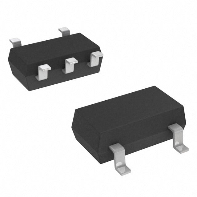
| 产品图片 |
|
| rohs | 符合RoHS无铅 / 符合限制有害物质指令(RoHS)规范要求 |
| 产品系列 | 放大器 IC,精密放大器,Analog Devices AD8613AKSZ-R2- |
| 数据手册 | |
| 产品型号 | AD8613AKSZ-R2 |
| 产品培训模块 | http://www.digikey.cn/PTM/IndividualPTM.page?site=cn&lang=zhs&ptm=30008http://www.digikey.cn/PTM/IndividualPTM.page?site=cn&lang=zhs&ptm=26202 |
| 产品种类 | 精密放大器 |
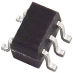
| 供应商器件封装 | SC-70-5 |
| 共模抑制比—最小值 | 95 dB |
| 关闭 | No |
| 其它名称 | AD8613AKSZ-R2CT |
| 包装 | 剪切带 (CT) |
| 压摆率 | 0.1 V/µs |
| 双重电源电压 | 0.9 V to 2.5 V |
| 可用增益调整 | 114 dB |
| 商标 | Analog Devices |
| 增益带宽生成 | 400 kHz |
| 增益带宽积 | 400kHz |
| 安装类型 | 表面贴装 |
| 安装风格 | SMD/SMT |
| 封装 | Reel |
| 封装/外壳 | 6-TSSOP(5 引线),SC-88A,SOT-353 |
| 封装/箱体 | SC-70-5 |
| 工作温度 | -40°C ~ 125°C |
| 工作电源电压 | 1.8 V to 5 V |
| 工厂包装数量 | 250 |
| 放大器类型 | 通用 |
| 最大双重电源电压 | 2.5 V |
| 最大工作温度 | + 125 C |
| 最小双重电源电压 | 0.9 V |
| 最小工作温度 | - 40 C |
| 标准包装 | 1 |
| 电压-电源,单/双 (±) | 1.8 V ~ 5 V, ±0.9 V ~ 2.5 V |
| 电压-输入失调 | 400µV |
| 电压增益dB | 113.98 dB |
| 电流-电源 | 38µA |
| 电流-输入偏置 | 0.2pA |
| 电流-输出/通道 | 80mA |
| 电源电压-最大 | 5 V |
| 电源电压-最小 | 1.8 V |
| 电源电流 | 38 uA |
| 电源类型 | Single, Dual |
| 电路数 | 1 |
| 系列 | AD8613 |
| 视频文件 | http://www.digikey.cn/classic/video.aspx?PlayerID=1364138032001&width=640&height=505&videoID=2245193153001http://www.digikey.cn/classic/video.aspx?PlayerID=1364138032001&width=640&height=505&videoID=2245193159001 |
| 转换速度 | 0.1 V/us |
| 输入偏压电流—最大 | 780 pA |
| 输入电压范围—最大 | 5 V |
| 输入补偿电压 | 400 uV |
| 输出类型 | Rail to Rail Input/Output |
| 通道数量 | 1 Channel |


- 商务部:美国ITC正式对集成电路等产品启动337调查
- 曝三星4nm工艺存在良率问题 高通将骁龙8 Gen1或转产台积电
- 太阳诱电将投资9.5亿元在常州建新厂生产MLCC 预计2023年完工
- 英特尔发布欧洲新工厂建设计划 深化IDM 2.0 战略
- 台积电先进制程称霸业界 有大客户加持明年业绩稳了
- 达到5530亿美元!SIA预计今年全球半导体销售额将创下新高
- 英特尔拟将自动驾驶子公司Mobileye上市 估值或超500亿美元
- 三星加码芯片和SET,合并消费电子和移动部门,撤换高东真等 CEO
- 三星电子宣布重大人事变动 还合并消费电子和移动部门
- 海关总署:前11个月进口集成电路产品价值2.52万亿元 增长14.8%


PDF Datasheet 数据手册内容提取
Low Cost Micropower, Low Noise CMOS Rail-to-Rail, Input/Output Operational Amplifiers Data Sheet AD8613/AD8617/AD8619 FEATURES PIN CONFIGURATIONS Offset voltage: 2.2 mV maximum Low input bias current: 1 pA maximum OUT 1 AD8613 5 V+ SLoinwg lneo-sisuep: p2l2y noVp/e√rHatzi on: 1.8 V to 5.5 V +VIN– 23 (NToOt Pto V SIEcWale) 4 –IN 05622-037 Micropower: 50 μA/amplifier maximum over temperature Figure 1. 5-Lead SC70 and 5-Lead TSOT-23 No phase reversal Unity gain stable OUTA 1 8 V+ AD8617 Qualified for automotive applications –INA 2 7 OUTB TOPVIEW APPLICATIONS +INVA– 34 (NottoScale) 65 –+IINNBB 05622-001 Battery-powered instrumentation Figure 2. 8-Lead MSOP and 8-Lead SOIC_N Multipole filters Current shunt sense OUT A 1 8 V+ Sensors –IN A 2 AD8617 7 OUT B ADC predrivers TOP VIEW +IN A 3 6 –IN B (Not to Scale) DAC drivers/level shifters V– 4 5 +IN B Low power ASIC input or output amplifiers GThEeN AEDR8A61L3 /DADES86C1R7/IAPDT8IO61N9 are single, dual, and quad micro- N1 . O PMTIUNESS 4T A BNED C TOHNEN EEXCPTOESDE TDO P VA–D. 05622-002 Figure 3. 8-Lead LFCSP power, rail-to-rail input and output amplifiers that feature low supply current, as well as low input voltage and current noise. OUT A 1 14 OUT D The parts are fully specified to operate from 1.8 V to 5 V single –INA 2 13 –IN D supply, or ±0.9 V and ±2.5 V dual supply. The combination of low +INA 3 AD8619 12 +IN D TOP VIEW noise, very low input bias currents, and low power consumption V+ 4 (Not to Scale) 11 V– make the AD8613/AD8617/AD8619 especially useful in portable +IN B 5 10 +IN C and loop-powered instrumentation. –IN B 6 9 –IN C The ability to swing rail-to-rail at both the input and output OUT B 7 8 OUT C05622-035 enables designers to buffer CMOS ADCs, DACs, ASICs, and Figure 4. 14-Lead TSSOP and 14-Lead SOIC other wide output swing devices in low power, single-supply systems. The AD8613 is available in a 5-lead SC70 package and a 5-lead TSOT-23 package. The AD8617 is available in 8-lead MSOP, 8-lead SOIC, and 8-lead LFCSP packages. The AD8619 is available in 14-lead TSSOP and 14-lead SOIC packages. The AD8617W is qualified for automotive applications and is available in 8-lead MSOP and 8-lead SOIC packages. The AD8619W is qualified for automotive applications and is available in 14-lead SOIC and 14-lead TSSOP packages. Rev. H Document Feedback Information furnished by Analog Devices is believed to be accurate and reliable. However, no responsibility is assumed by Analog Devices for its use, nor for any infringements of patents or other One Technology Way, P.O. Box 9106, Norwood, MA 02062-9106, U.S.A. rights of third parties that may result from its use. Specifications subject to change without notice. No license is granted by implication or otherwise under any patent or patent rights of Analog Devices. Tel: 781.329.4700 ©2005–2016 Analog Devices, Inc. All rights reserved. Trademarks and registered trademarks are the property of their respective owners. Technical Support www.analog.com
AD8613/AD8617/AD8619 Data Sheet TABLE OF CONTENTS Features .............................................................................................. 1 Thermal Resistance .......................................................................5 Applications ....................................................................................... 1 ESD Caution...................................................................................5 General Description ......................................................................... 1 Typical Performance Characteristics ..............................................6 Pin Configurations ........................................................................... 1 Outline Dimensions ....................................................................... 12 Revision History ............................................................................... 2 Ordering Guide .......................................................................... 15 Specifications ..................................................................................... 3 Automotive Products ................................................................. 16 Absolute Maximum Ratings ............................................................ 5 REVISION HISTORY 5/2016—Rev. G to Rev. H Changes to Input Characteristics, Input Voltage Range Parameter; Changed CP-8-9 to CP-8-21 ........................................ Throughout Dynamic Performance, Settling Time to 0.1% and Phase Margin Changed LFCSP_VD to LFCSP ................................... Throughout Parameters; and Noise Performance, Peak-to-Peak Noise Changes to Figure 3 .......................................................................... 1 Parameter, Table 1 ............................................................................. 3 Changes to Table 4 ............................................................................ 5 Changes to Input Characteristics, Input Voltage Range Parameter; Changes to Figure 43 ...................................................................... 15 Dynamic Performance, Settling Time to 0.1% and Phase Margin Updated Outline Dimensions ....................................................... 15 Parameters; and Noise Performance, Peak-to-Peak Noise Changes to Ordering Guide .......................................................... 15 Parameter, Table 2 ............................................................................. 4 Changes to Table 3 and Table 4 ....................................................... 5 12/2014—Rev. F to Rev. G Changes to Figure 12 to Figure 15 .................................................. 7 Changes to General Description Section ...................................... 1 Changes to Figure 18 Caption ......................................................... 8 Changes to Ordering Guide .......................................................... 15 Changes to Figure 30 and Figure 31 ............................................ 10 Updated Outline Dimensions ....................................................... 12 4/2014—Rev. E to Rev. F Added Figure 44; Renumbered Sequentially .............................. 14 Changes to General Description Section ...................................... 1 Changes to Ordering Guide .......................................................... 15 Changes to Table 3 ............................................................................ 5 Changes to Ordering Guide .......................................................... 15 1/2006—Rev. A to Rev. B Added Automotive Products Section .......................................... 15 Added AD8613 .................................................................... Universal Changes to Features .......................................................................... 1 3/2010—Rev. D to Rev. E Changes to Table 1 ............................................................................. 3 Changes to General Description .................................................... 1 Changes to Table 2 ............................................................................. 4 Changes to Ordering Guide .......................................................... 15 Updated Outline Dimensions ....................................................... 12 Changes to Ordering Guide .......................................................... 13 3/2010—Rev. C to Rev. D Changes to General Description .................................................... 1 10/2005—Rev. 0 to Rev. A Changes to Ordering Guide .......................................................... 15 Added AD8619 .................................................................... Universal Change to Specifications Section .................................................... 3 10/2009—Rev. B to Rev. C Updated Outline Dimensions ....................................................... 12 Added 8-Lead LFCSP Package .......................................... Universal Changes to Ordering Guide .......................................................... 13 Changes to Features Section, Figure 2 Caption, General Description Section, and Figure 3 ................................... 1 9/2005—Revision 0: Initial Version Changed V to V Throughout ...................................................... 3 S SY Rev. H | Page 2 of 16
Data Sheet AD8613/AD8617/AD8619 SPECIFICATIONS Electrical characteristics at V = 5 V, V = V /2, T = 25°C, unless otherwise noted. SY CM SY A Table 1. Parameter Symbol Conditions Min Typ Max Unit INPUT CHARACTERISTICS Offset Voltage V −0.3 V < V < +5.3 V 0.4 2.2 mV OS CM −40°C < T < +125°C, −0.3 V < V < +5.2 V 2.2 mV A CM Offset Voltage Drift ∆V /∆T −40°C < T < +125°C 1 4.5 μV/°C OS A AD8613 2.5 7.0 μV/°C Input Bias Current I 0.2 1 pA B −40°C < T < +85°C 110 pA A −40°C < T < +125°C 780 pA A Input Offset Current I 0.1 0.5 pA OS −40°C < T < +85°C 50 pA A −40°C < T < +125°C 250 pA A Input Voltage Range IVR 0 5 V Common-Mode Rejection Ratio CMRR 0 V < V < 5 V 95 dB CM −40°C < T < +125°C 68 dB A Large Signal Voltage Gain A R = 10 kΩ, 0.5 V < V < 4.5 V 235 500 V/mV VO L O Input Capacitance C 1.9 pF DIFF C 2.5 pF CM OUTPUT CHARACTERISTICS Output Voltage High V I = 1 mA 4.95 4.98 V OH L −40°C to +125°C 4.9 V I = 10 mA 4.7 V L −40°C to +125°C 4.50 V Output Voltage Low V I = 1 mA 20 30 mV OL L −40°C to +125°C 50 mV I = 10 mA 190 275 mV L −40°C to +125°C 335 mV Short-Circuit Current I ±80 mA SC Closed-Loop Output Impedance Z f = 10 kHz, A = 1 15 Ω OUT V POWER SUPPLY Power Supply Rejection Ratio PSRR 1.8 V < V < 5 V 67 94 dB SY −40°C < T < +125°C 64 dB A Supply Current/Amplifier I V = V /2 38 μA SY O SY −40°C <T < +125°C 50 μA A DYNAMIC PERFORMANCE Slew Rate SR R = 10 kΩ 0.1 V/μs L Settling Time to 0.1% t G = ±1, V = 2 V step, C = 20 pF, R = 1 kΩ 23 μs S IN L L Gain Bandwidth Product GBP R = 100 kΩ 400 kHz L R = 10 kΩ 350 kHz L Phase Margin Ø R = 10 kΩ, R = 100 kΩ, C = 20 pF 70 Degrees M L L L NOISE PERFORMANCE Peak-to-Peak Noise e p-p 0.1 Hz to 10 Hz 2.3 3.5 μV n Voltage Noise Density e f = 1 kHz 25 nV/√Hz n f = 10 kHz 22 nV/√Hz Current Noise Density i f = 1 kHz 0.05 pA/√Hz n Rev. H | Page 3 of 16
AD8613/AD8617/AD8619 Data Sheet Electrical characteristics at V = 1.8 V, V = V /2, T = 25°C, unless otherwise noted. SY CM SY A Table 2. Parameter Symbol Conditions Min Typ Max Unit INPUT CHARACTERISTICS Offset Voltage V −0.3 V < V < +1.9 V 0.4 2.2 mV OS CM −0.3 V < V < +1.8 V; −40°C < T < +125°C 2.2 mV CM A Offset Voltage Drift ∆V /∆T −40°C < T < +125°C 1 8.5 μV/°C OS A AD8613 3.7 9.0 μV/°C Input Bias Current I 0.2 1 pA B −40°C < T < +85°C 110 pA A −40°C < T < +125°C 780 pA A Input Offset Current I 0.1 0.5 pA OS −40°C < T < +85°C 50 pA A −40°C < T < +125°C 250 pA A Input Voltage Range IVR 0 1.8 V Common-Mode Rejection Ratio CMRR 0 V < V < 1.8 V 58 86 dB CM −40°C < T < +125°C 55 dB A Large Signal Voltage Gain A R = 10 kΩ, 0.5 V < V < 1.3 V 85 1000 V/mV VO L O Input Capacitance C 2.1 pF DIFF C 3.8 pF CM OUTPUT CHARACTERISTICS Output Voltage High V I = 1 mA 1.65 1.73 V OH L −40°C to +125°C 1.6 V Output Voltage Low V I = 1 mA 44 60 mV OL L −40°C to +125°C 80 mV Short-Circuit Current I ±7 mA SC Closed-Loop Output Impedance Z f = 10 kHz, A = 1 15 Ω OUT V POWER SUPPLY Power Supply Rejection Ratio PSRR 1.8 V < V < 5 V 67 94 dB S Supply Current/Amplifier I V = V /2 38 μA SY O SY −40°C <T < +125°C 50 μA A DYNAMIC PERFORMANCE Slew Rate SR R = 10 kΩ 0.1 V/μs L Settling Time to 0.1% t G = ±1, V = 1 V step, C = 20 pF, R = 1 kΩ 6.5 μs S IN L L Gain Bandwidth Product GBP R = 100 kΩ 400 kHz L R = 10 kΩ 350 kHz L Phase Margin Ø R = 10 kΩ, R = 100 kΩ, C = 20 pF 70 Degrees M L L L NOISE PERFORMANCE Peak-to-Peak Noise e p-p 0.1 Hz to 10 Hz 2.3 3.5 μV n Voltage Noise Density e f = 1 kHz 25 nV/√Hz n f = 10 kHz 22 nV/√Hz Current Noise Density i f = 1 kHz 0.05 pA/√Hz n Rev. H | Page 4 of 16
Data Sheet AD8613/AD8617/AD8619 ABSOLUTE MAXIMUM RATINGS THERMAL RESISTANCE T = 25°C, unless otherwise noted. A θ is specified for the worst-case conditions, that is, a device JA Table 3. soldered in a circuit board for surface-mount packages. Parameter Rating Supply Voltage 6 V Table 4. Thermal Characteristics Input Voltage V − 0.3 V to V + 0.3 V Package Type θ θ Unit SS DD JA JC Input Current ±10 mA 5-Lead TSOT-23 (UJ-5) 207 61 °C/W Differential Input Voltage ±6 V 5-Lead SC70 (KS-5) 376 126 °C/W Output Short-Circuit Duration to GND Indefinite 8-Lead MSOP (RM-8) 210 45 °C/W Storage Temperature Range −65°C to +150°C 8-Lead SOIC_N (R-8) 158 43 °C/W Operating Temperature Range −40°C to +125°C 8-Lead LFCSP (CP-8-21) 81 20 °C/W Junction Temperature Range −65°C to +150°C 14-Lead SOIC_N (R-14) 120 36 °C/W Lead Temperature (Soldering, 60 sec) 300°C 14-Lead TSSOP (RU-14) 180 35 °C/W ESD AD8613 HBM ±4000 V ESD CAUTION FICDM ±1000 V ESD AD8617 HBM ±3000 V FICDM ±1000 V MM ±100 V ESD AD8619 HBM ±4000 V FICDM ±1250 V MM ±200 V Stresses at or above those listed under Absolute Maximum Ratings may cause permanent damage to the product. This is a stress rating only; functional operation of the product at these or any other conditions above those indicated in the operational section of this specification is not implied. Operation beyond the maximum operating conditions for extended periods may affect product reliability. Rev. H | Page 5 of 16
AD8613/AD8617/AD8619 Data Sheet TYPICAL PERFORMANCE CHARACTERISTICS V = 5 V or ±2.5 V, unless otherwise noted. SY 1800 400 1600 –VT0AS.Y 5= V= 2 <55 °.V5CVCM < +5.5V 350 VSY = 5V AND 1.8V 1400 S A) 300 R p LIFIE1200 ENT ( 250 MP1000 RR FA CU 200 O 800 S R A E BI 150 NUMB 600 NPUT 100 400 I 2000 05622-003 500 05622-006 0 0 0 0 0 0 0 0 0 0 0 0 0 0 25 50 75 100 125 150 0 0 0 0 0 0 0 0 0 0 0 0 0 0 –20 –17 –14 –11 –8 –5 –2 1 4 7 10 13 16 19 TEMPERATURE (°C) INPUT OFFSET VOLTAGE (µV) Figure 5. Input Offset Voltage Distribution Figure 8. Input Bias Current vs. Temperature 40 50 –V4C0M° C= <2 .T5VA < 125°C TA = 25°C 35 40 S 30 AMPLIFIER 2250 RRENT (µA) 30 F U O C R Y 20 BE 15 PL NUM 10 SUP 10 05 05622-004 0 05622-007 0 1 2 3 4 5 6 7 8 9 10 0 1 2 3 5 TCVOS (µV/°C) SUPPLY VOLTAGE (V) Figure 6. Input Offset Voltage Drift Distribution Figure 9. Supply Current vs. Supply Voltage 2000 VTASY = = 2 55°VC 50 VSY =±2.5V,±1.35V,±0.9V 1500 A) E (µV) 1000 ER ( 40 G FI FFSET VOLTA –5500000 RRENT/AMPLI 3200 O U UT Y C P–1000 L N P I UP 10 ––12050000 05622-005 S 0 05622-008 –0.5 0 0.5 1.0 1.5 2.0 2.5 3.0 3.5 4.0 4.5 5.0 5.5 –40 –10 20 50 80 110 INPUT COMMON MODE VOLTAGE (V) TEMPERATURE (°C) Figure 7. Input Offset Voltage vs. Input Common-Mode Voltage Figure 10. Supply Current vs. Temperature Rev. H | Page 6 of 16
Data Sheet AD8613/AD8617/AD8619 1k 60 135 VSY = 5V mV) TA = 25ºC 50 L ( 100 AI VSY – VOH 40 90 OLTAGETO SUPPLY R 101 SOURCESINK PEN-LOOP GAIN (dB) 321000 ΦM 45 PHASE (Degrees) V O PUT 0.1 VOL 0 0 OUT 0.001.001 0.01 LOAD CUR0.R1ENT (mA) 1 1005622-009 ––21001k RCVSLLY == = 12 00±0p2k.F5ΩVAND 1±00k.9FVREQUENCY (Hz)100k 1M–45 05622-012 Figure 11. Output Voltage to Supply Rail vs. Load Current Figure 14. Open-Loop Gain and Phase vs. Frequency 40 120 VSY = 5V VSY = 5V AND 2.7V V) TA = 25°C m L ( 100 AI 30 Y R VSY – VOH @ 1mA L 80 P P AGETO SU 20 VOL @ 1mA CMRR (dB) 60 T OL 40 V T 10 U P T 20 OU 0 05622-010 0 05622-013 –40 –25 –10 5 20 35 50 65 80 95 110 125 100 1k 10k 100k 1M TEMPERATURE (°C) FREQUENCY (Hz) Figure 12. Output Voltage to Supply Rail vs. Temperature Figure 15. CMRR vs. Frequency (IL = 1 mA) 350 120 VSY = 5V VSY =±2.5V AND±1.35V V) TA = 25°C m 300 AIL ( VSY – VOH @ 10mA 100 Y R 250 PL 80 P GETO SU 210500 VOL @ 10mA SRR (dB) 60 A P T OL 40 V 100 T U P OUT 500 05622-011 200 05622-014 –40 –25 –10 5 20 35 50 65 80 95 110 125 100 1k 10k 100k 1M TEMPERATURE (°C) FREQUENCY(Hz) Figure 13. Output Voltage to Supply Rail vs. Temperature Figure 16. PSRR vs. Frequency (IL = 10 mA) Rev. H | Page 7 of 16
AD8613/AD8617/AD8619 Data Sheet 1k VSY = 5V AV = 100 ARVL == 110kΩ CL = 200pF Ω) 100 CE ( V) MPEDAN 10 AV = 10 AV = 1 GE (1V/DI UT I LTA P O UT V O 1 0100 1k 10k VS1Y00 =k 5VAND 1.8V1M05622-015 TIME (20µs/DIV) 05622-018 FREQUENCY (Hz) Figure 17. Output Impedance vs. Frequency Figure 20. Large Signal Transient Response 50 VSY = 5V 45 TA = 25°C 0 %) 40 V) HOOT ( 35 V (OUT VASVY = = – ±520.5V RS 30 –2.5 VE –OS O 25 L A N 20 G 100 SI L 15 V) L m MA 10 (N S +OS VI 50 05622-016 0 05622-019 10 100 1000 TIME (20µs/DIV) LOAD CAPACITANCE (pF) Figure 18. Small Signal Overshoot vs. Load Capacitance Figure 21. Positive Overload Recovery AVSVY = = 1 5V, 2.7V, 1.8V 2.5 VASVY = = – ±520.5V RL = 10kΩ CL = 200pF V) (UT DIV) VO V/ 0 m 0 5 E ( G A LT 0 O V V) m (N VI 05622-017 –100 05622-020 TIME (4µs/DIV) TIME (20µs/DIV) Figure 19. Small Signal Transient Response Figure 22. Negative Overload Recovery Rev. H | Page 8 of 16
Data Sheet AD8613/AD8617/AD8619 1000 VIN TVASY = = 2 55ºVC Hz) V) VOUT E (nV/ 100 E (1V/DI GE NOIS G A A T T L OL VO 10 1/F CORNER @ 100Hz V T U P N VSY = ±2.5V I AVRIVLN === 1160Vk Ωp-p 05622-021 11 10 100 1000 1000005622-023 TIME (20ms/DIV) FREQUENCY (Hz) Figure 23. No Phase Reversal Figure 25. Voltage Noise Density 140 VSY = 5VAND 2.7V VSY = 5V 120 DIV) N (dB) 100 V/ O E (1µ RATI 80 S A GE NOI EL SEP 60 A N VOLT CHAN 40 20 05622-022 0 05622-024 TIME (1s/DIV) 100 1k 10k 100k 1M FREQUENCY (Hz) Figure 24. 0.1 Hz to 10 Hz Input Voltage Noise Figure 26. Channel Separation Rev. H | Page 9 of 16
AD8613/AD8617/AD8619 Data Sheet V = 1.8 V or ±0.9 V, unless otherwise noted. SY 450 80 VSY = 1.8V VSY = 1.8V 400 0V < VCM < 1.8V V) PLIFIERS 335000 TA = 25°C UPPLY RAIL (m 60 VSY–VOH @ 1mA M 250 S FA TO 40 O 200 E UMBER 150 VOLTAG VOH @ 1mA N 100 UT 20 P T 500 05622-025 OU 0 05622-028 0 0 0 0 0 0 0 0 0 0 0 0 0 0 –40 –25 –10 5 20 35 50 65 80 95 110 125 0 0 0 0 0 0 0 0 0 0 0 0 0 0 –20 –17 –14 –11 –8 –5 –2 1 4 7 10 13 16 19 TEMPERATURE (°C) INPUT OFFSET VOLTAGE (µV) Figure 27. Input Offset Voltage Distribution Figure 30. Output Voltage to Supply Rail vs. Temperature (IL = 1 mA) 2000 100 VSY = 1.8V VSY = 1.8V 1500 TA = 25°C TA = 25°C µV) 1000 80 E ( G A 500 T VOLT 0 R (dB) 60 E R S M FF –500 C 40 O T U P–1000 N I 20 ––12500000 05622-026 0 05622-029 –0.5 –0.2 0.1 0.4 0.7 1.0 1.3 1.6 1.9 2.2 100 1k 10k 100k 1M INPUT COMMON-MODE VOLTAGE (V) FREQUENCY (Hz) Figure 28. Input Offset Voltage vs. Input Common-Mode Voltage Figure 31. CMRR vs. Frequency 1000 120 mV) VTASY = = 2 51°.8CV VTAS Y= = 2 51°.8CV L ( 100 100 AI VSY–VOH R Y SUPPL 10 SOURCE B) 80 TO R (d 60 E R AG 1 PS OLT SINK 40 T V VOL PU 0.1 T 20 OU 0.01 05622-027 0 05622-030 0.001 0.01 0.1 1 10 100 1k 10k 1M LOAD CURRENT (mA) FREQUENCY (Hz) Figure 29. Output Voltage to Supply Rail vs. Load Current Figure 32. PSRR vs. Frequency Rev. H | Page 10 of 16
Data Sheet AD8613/AD8617/AD8619 40 TVAS Y= = 2 51°.8CV VSY = 1.8V %) T ( 30 O HO V) S DI AL OVER 20 –OS GE (1µV/ N A SIG OLT L V AL 10 +OS M S 0 05622-031 05622-033 10 100 1k TIME (1s/DIV) LOAD CAPACITANCE (pF) Figure 33. Small Signal Overshoot vs. Load Capacitance Figure 35. 0.1 Hz to 10 Hz Input Voltage Noise 1k VASVY = = 1 1.8V TVASY = = 2 51°.8CV RCLL == 1200k0pΩF Hz) V/ mV/DIV) OISE (n 100 OLTAGE (500 T VOLTAGE N 10 1/F CORNER @ 100Hz V U P N I 05622-032 11 10 100 1k 10k05622-034 TIME (20µs/DIV) FREQUENCY (Hz) Figure 34. Large Signal Transient Response Figure 36. Voltage Noise Density Rev. H | Page 11 of 16
AD8613/AD8617/AD8619 Data Sheet OUTLINE DIMENSIONS 3.20 3.00 2.80 8 5 5.15 3.20 4.90 3.00 4.65 2.80 1 4 PIN 1 IDENTIFIER 0.65 BSC 0.95 15° MAX 0.85 1.10 MAX 0.75 0.80 0.15 0.40 6° 0.23 0.55 CO0P.0L50A.1N0ARICTOYMPLIANT0. 2T5O JEDEC STA0°NDARDS 0M.0O9-187-AA 0.40 10-07-2009-B Figure 37. 8-Lead Mini Small Outline Package [MSOP] (RM-8) Dimensions shown in millimeters 5.00(0.1968) 4.80(0.1890) 8 5 4.00(0.1574) 6.20(0.2441) 3.80(0.1497) 1 4 5.80(0.2284) 1.27(0.0500) 0.50(0.0196) BSC 1.75(0.0688) 0.25(0.0099) 45° 0.25(0.0098) 1.35(0.0532) 8° 0.10(0.0040) 0° COPLANARITY 0.51(0.0201) 0.10 SEATING 0.31(0.0122) 0.25(0.0098) 10..2470((00..00510507)) PLANE 0.17(0.0067) COMPLIANTTOJEDECSTANDARDSMS-012-AA C(RINOEFNPEATRRREOENNLCLTEIHNEOGSNDELISYM)AEANNRDSEIAORRNOESUNANORDETEDAIN-POMPFRIFLOLMPIMIRLELIATIMTEEERTFSEO;RIRNECUQHSUEDIVIINMAELDENENSSTIIOGSNNFS.OR 012407-A Figure 38. 8-Lead Standard Small Outline Package [SOIC_N] Narrow Body (R-8) Dimensions shown in millimeters and (inches) Rev. H | Page 12 of 16
Data Sheet AD8613/AD8617/AD8619 8.75 (0.3445) 8.55 (0.3366) 4.00 (0.1575) 14 8 6.20 (0.2441) 3.80 (0.1496) 1 7 5.80 (0.2283) 1.27 (0.0500) 0.50 (0.0197) BSC 45° 1.75 (0.0689) 0.25 (0.0098) 0.25 (0.0098) 1.35 (0.0531) 8° 0.10 (0.0039) 0° COPLANARITY SEATING 0.10 0.51 (0.0201) PLANE 0.25 (0.0098) 1.27 (0.0500) 0.31 (0.0122) 0.17 (0.0067) 0.40 (0.0157) COMPLIANTTO JEDEC STANDARDS MS-012-AB C(RINOEFNPEATRRREOENNLCLTEIHN EOGSN DELSIYM)AEANNRDSEI AORRNOESU NANORDEET DAIN-PO MPFRIFLO LMPIIMRLELIATIMTEEER TFSEO; RIRN ECUQHSU EDI VIINMA LEDENENSSTIIOGSN NFS.OR 060606-A Figure 39. 14-Lead Standard Small Outline Package [SOIC_N] Narrow Body (R-14) Dimensions shown in millimeters and (inches) 5.10 5.00 4.90 14 8 4.50 4.40 6.40 BSC 4.30 1 7 PIN 1 0.65 BSC 1.05 1.00 1M.A20X 0.20 0.80 0.09 0.75 0.15 8° 0.60 0.05 0.30 SPELAATNIENG 0° 0.45 COPLANARITY 0.19 0.10 COMPLIANT TO JEDEC STANDARDS MO-153-AB-1 061908-A Figure 40. 14-Lead Thin Shrink Small Outline Package [TSSOP] (RU-14) Dimensions shown in millimeters Rev. H | Page 13 of 16
AD8613/AD8617/AD8619 Data Sheet 2.20 2.00 1.80 1.35 5 4 2.40 1.25 2.10 1.15 1 2 3 1.80 0.65BSC 1.00 1.10 0.40 0.90 0.80 0.10 0.70 0.46 0.10MAX 0.30 SPLEAATNIENG 00..2028 0.36 COPLANARITY 0.15 0.26 0.10 COMPLIANTTOJEDECSTANDARDSMO-203-AA 072809-A Figure 41. 5-Lead Thin Shrink Small Outline Transistor Package [SC70] (KS-5) Dimensions shown in millimeters 2.90 BSC 5 4 1.60 BSC 2.80 BSC 1 2 3 0.95 BSC 1.90 *0.90 MAX BSC 0.70 MIN *1.00 MAX 0.20 0.08 8° 0.10 MAX 0.50 SEATING 4° 0.60 0.30 PLANE 0° 0.45 0.30 *CTHOEM PELXICAENPTT TIOON J OEDF EPCA CSTKAANGDEA HREDIGS HMTO A-1N9D3 -TAHBICWKINTHESS. 100708-A Figure 42. 5-Lead Thin Small Outline Transistor Package [TSOT-23] (UJ-5) Dimensions shown in millimeters Rev. H | Page 14 of 16
Data Sheet AD8613/AD8617/AD8619 2.54 2.44 3.10 2.34 3.00 SQ 0.50 BSC 2.90 5 8 PIN 1 INDEX EXPOSED 1.70 AREA PAD 1.60 0.50 1.50 0.40 0.30 0.20 MIN 4 1 TOP VIEW BOTTOM VIEW PIN 1 INDICATOR (R 0.20) 0.80 0.75 0.05 MAX FTOHER EPXRPOOPSEERD C POANDN, ERCETFIEORN TOOF 0.70 0.02 NOM THE PIN CONFIGURATION AND FUNCTION DESCRIPTIONS PKG-004371 SEPALTAINNGE 000...322050 0.203 REF SECTION OF THIS DATA SHEET. 12-03-2013-A Figure 43. 8-Lead Lead Frame Chip Scale Package [LFCSP] 3 mm × 3 mm Body and 0.75 mm Package Height (CP-8-21) Dimensions shown in millimeters ORDERING GUIDE Model1, 2 Temperature Range Package Description Package Option Branding AD8613AKSZ-R2 −40°C to +125°C 5-Lead SC70 KS-5 A0Y AD8613AKSZ-REEL −40°C to +125°C 5-Lead SC70 KS-5 A0Y AD8613AKSZ-REEL7 −40°C to +125°C 5-Lead SC70 KS-5 A0Y AD8613AUJZ-R2 −40°C to +125°C 5-Lead TSOT-23 UJ-5 A0Y AD8613AUJZ-REEL −40°C to +125°C 5-Lead TSOT-23 UJ-5 A0Y AD8613AUJZ-REEL7 −40°C to +125°C 5-Lead TSOT-23 UJ-5 A0Y AD8617ACPZ-R2 −40°C to +125°C 8-Lead LFCSP CP-8-21 A0T AD8617ACPZ-R7 −40°C to +125°C 8-Lead LFCSP CP-8-21 A0T AD8617ARMZ −40°C to +125°C 8-Lead MSOP RM-8 A0T AD8617ARMZ-REEL −40°C to +125°C 8-Lead MSOP RM-8 A0T AD8617ARZ −40°C to +125°C 8-Lead SOIC_N R-8 AD8617ARZ-REEL −40°C to +125°C 8-Lead SOIC_N R-8 AD8617ARZ-REEL7 −40°C to +125°C 8-Lead SOIC_N R-8 AD8617WARMZ-REEL −40°C to +125°C 8-Lead MSOP RM-8 A23 AD8617WARZ-RL −40°C to +125°C 8-Lead SOIC_N R-8 AD8617WARZ-R7 −40°C to +125°C 8-Lead SOIC_N R-8 AD8619ARUZ −40°C to +125°C 14-Lead TSSOP RU-14 AD8619ARUZ-REEL −40°C to +125°C 14-Lead TSSOP RU-14 AD8619ARZ −40°C to +125°C 14-Lead SOIC_N R-14 AD8619ARZ-REEL7 −40°C to +125°C 14-Lead SOIC_N R-14 AD8619WARZ-RL −40°C to +125°C 14-Lead SOIC_N R-14 AD8619WARZ-R7 −40°C to +125°C 14-Lead SOIC_N R-14 AD8619WARUZ-R7 −40°C to +125°C 14-Lead TSSOP RU-14 AD8619WARUZ-RL −40°C to +125°C 14-Lead TSSOP RU-14 1 Z = RoHS Compliant Part. 2 W = Qualified for Automotive Applications. Rev. H | Page 15 of 16
AD8613/AD8617/AD8619 Data Sheet AUTOMOTIVE PRODUCTS The AD8617W and AD8619W models are available with controlled manufacturing to support the quality and reliability requirements of automotive applications. Note that these automotive models may have specifications that differ from the commercial models; therefore, designers should review the Specifications section of this data sheet carefully. Only the automotive grade products shown are available for use in automotive applications. Contact your local Analog Devices account representative for specific product ordering information and to obtain the specific Automotive Reliability reports for these models. ©2005–2016 Analog Devices, Inc. All rights reserved. Trademarks and registered trademarks are the property of their respective owners. D05622-0-5/16(H) Rev. H | Page 16 of 16