ICGOO在线商城 > 集成电路(IC) > 线性 - 放大器 - 仪表,运算放大器,缓冲器放大器 > AD8602ARZ-REEL7
 Datasheet下载
- 型号: AD8602ARZ-REEL7
- 制造商: Analog
- 库位|库存: xxxx|xxxx
- 要求:
| 数量阶梯 | 香港交货 | 国内含税 |
| +xxxx | $xxxx | ¥xxxx |
查看当月历史价格
查看今年历史价格
AD8602ARZ-REEL7产品简介:
ICGOO电子元器件商城为您提供AD8602ARZ-REEL7由Analog设计生产,在icgoo商城现货销售,并且可以通过原厂、代理商等渠道进行代购。 AD8602ARZ-REEL7价格参考¥4.75-¥5.93。AnalogAD8602ARZ-REEL7封装/规格:线性 - 放大器 - 仪表,运算放大器,缓冲器放大器, General Purpose Amplifier 2 Circuit Rail-to-Rail 8-SOIC。您可以下载AD8602ARZ-REEL7参考资料、Datasheet数据手册功能说明书,资料中有AD8602ARZ-REEL7 详细功能的应用电路图电压和使用方法及教程。
AD8602ARZ-REEL7是Analog Devices Inc.生产的一款双通道、低失调、低噪声、精密CMOS运算放大器,属于线性放大器类别中的运算放大器产品。该器件具有轨至轨输入和输出(RRIO)能力、宽电源电压范围(2.7V至5.5V)、低静态电流以及出色的直流精度,适用于对信号完整性要求较高的应用场景。

典型应用包括:便携式医疗设备(如血糖仪、心电图设备),工业传感器信号调理(如压力、温度传感器的放大与处理),数据采集系统,高精度测量仪器,以及电池供电设备等。其低输入偏置电流和低噪声特性使其非常适合用于高阻抗传感器接口和微弱信号放大。此外,AD8602ARZ-REEL7采用SOIC-8封装,适合自动化贴片生产,广泛应用于需要小型化和高可靠性的电子系统中。

由于其优异的温度稳定性和长期漂移性能,该型号也常用于环境条件多变的工业控制和自动化领域。总之,AD8602ARZ-REEL7是一款适用于精密模拟信号处理的高性能运算放大器,特别适合注重功耗、精度和稳定性的小型化电子设备。
| 参数 | 数值 |
| -3db带宽 | - |
| 产品目录 | 集成电路 (IC)半导体 |
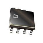
| 描述 | IC OPAMP GP 8.4MHZ RRO 8SOIC精密放大器 RRIO Dual w/ Low Offset VTG |
| 产品分类 | Linear - Amplifiers - Instrumentation, OP Amps, Buffer Amps集成电路 - IC |
| 品牌 | Analog Devices Inc |
| 产品手册 | |
| 产品图片 |
|
| rohs | 符合RoHS无铅 / 符合限制有害物质指令(RoHS)规范要求 |
| 产品系列 | 放大器 IC,精密放大器,Analog Devices AD8602ARZ-REEL7DigiTrim® |
| 数据手册 | |
| 产品型号 | AD8602ARZ-REEL7 |
| 产品培训模块 | http://www.digikey.cn/PTM/IndividualPTM.page?site=cn&lang=zhs&ptm=12927http://www.digikey.cn/PTM/IndividualPTM.page?site=cn&lang=zhs&ptm=30008http://www.digikey.cn/PTM/IndividualPTM.page?site=cn&lang=zhs&ptm=26202 |
| 产品种类 | 精密放大器 |
| 供应商器件封装 | 8-SOIC |
| 共模抑制比—最小值 | 89 dB |
| 关闭 | No |
| 其它名称 | AD8602ARZ-REEL7DKR |
| 包装 | Digi-Reel® |
| 压摆率 | 6 V/µs |
| 可用增益调整 | 100 dB |
| 商标 | Analog Devices |
| 增益带宽生成 | 8.4 MHz |
| 增益带宽积 | 8.4MHz |
| 安装类型 | 表面贴装 |
| 安装风格 | SMD/SMT |
| 封装 | Reel |
| 封装/外壳 | 8-SOIC(0.154",3.90mm 宽) |
| 封装/箱体 | SOIC-8 |
| 工作温度 | -40°C ~ 125°C |
| 工作电源电压 | 2.7 V to 5.5 V |
| 工厂包装数量 | 1000 |
| 放大器类型 | 通用 |
| 最大工作温度 | + 125 C |
| 最小工作温度 | - 40 C |
| 标准包装 | 1 |
| 电压-电源,单/双 (±) | 2.7 V ~ 5.5 V |
| 电压-输入失调 | 80µV |
| 电压增益dB | 98.06 dB |
| 电流-电源 | 750µA |
| 电流-输入偏置 | 0.2pA |
| 电流-输出/通道 | 50mA |
| 电源电压-最大 | 5.5 V |
| 电源电压-最小 | 2.7 V |
| 电源电流 | 750 uA |
| 电源类型 | Single |
| 电路数 | 2 |
| 系列 | AD8602 |
| 视频文件 | http://www.digikey.cn/classic/video.aspx?PlayerID=1364138032001&width=640&height=505&videoID=2245193153001http://www.digikey.cn/classic/video.aspx?PlayerID=1364138032001&width=640&height=505&videoID=2245193159001 |
| 转换速度 | 6 V/us |
| 输入偏压电流—最大 | 1000 pA |
| 输入电压范围—最大 | 5 V |
| 输入补偿电压 | 80 uV |
| 输出电流 | 50 mA |
| 输出类型 | 满摆幅 |
| 通道数量 | 2 Channel |


- 商务部:美国ITC正式对集成电路等产品启动337调查
- 曝三星4nm工艺存在良率问题 高通将骁龙8 Gen1或转产台积电
- 太阳诱电将投资9.5亿元在常州建新厂生产MLCC 预计2023年完工
- 英特尔发布欧洲新工厂建设计划 深化IDM 2.0 战略
- 台积电先进制程称霸业界 有大客户加持明年业绩稳了
- 达到5530亿美元!SIA预计今年全球半导体销售额将创下新高
- 英特尔拟将自动驾驶子公司Mobileye上市 估值或超500亿美元
- 三星加码芯片和SET,合并消费电子和移动部门,撤换高东真等 CEO
- 三星电子宣布重大人事变动 还合并消费电子和移动部门
- 海关总署:前11个月进口集成电路产品价值2.52万亿元 增长14.8%


PDF Datasheet 数据手册内容提取
Precision CMOS, Single-Supply, Rail-to-Rail, Input/Output Wideband Operational Amplifiers AD8601/AD8602/AD8604 FEATURES PIN CONFIGURATIONS Low offset voltage: 500 μV maximum OUT A 1 5 V+ Single-supply operation: 2.7 V to 5.5 V AD8601 Low supply current: 750 μA/Amplifier V– 2 TOP VIEW (Not to Scale) WSleidwe rbaaten:d 5w Vid/μths : 8 MHz +IN 3 4 –IN 01525-001 Figure 1. 5-Lead SOT-23 (RJ Suffix) Low distortion No phase reversal OUT A 1 8 V+ Low input currents –IN A 2 AD8602 7 OUT B TOP VIEW UQnuiatlyif-igeadi nfo srt aabulteo motive applications +INV A– 34 (Not to Scale) 65 –+IINN BB 01525-002 APPLICATIONS Figure 2. 8-Lead MSOP (RM Suffix) and 8-Lead SOIC (R-Suffix) Current sensing OUT A 1 14 OUT D Barcode scanners –IN A 2 13 –IN D PA controls +IN A 3 AD8604 12 +IN D Battery-powered instrumentation V+ 4 (NToOt Pto V SIEcWale) 11 V– Multipole filters +IN B 5 10 +IN C Sensors –IN B 6 9 –IN C AAuSIdCi oin put or output amplifiers OUT B 7 8 OUT C 01525-003 Figure 3. 14-Lead TSSOP (RU Suffix) and 14-Lead SOIC (R Suffix) GENERAL DESCRIPTION OUT A 1 16 OUT D The AD8601, AD8602, and AD8604 are single, dual, and quad –IN A 2 15 –IN D rail-to-rail, input and output, single-supply amplifiers featuring +IN A 3 AD8604 14 +IN D very low offset voltage and wide signal bandwidth. These amplifiers TOP VIEW use a new, patented trimming technique that achieves superior V+ 4 (Not to Scale) 13 V– +IN B 5 12 +IN C performance without laser trimming. All are fully specified to –IN B 6 11 –IN C operate on a 3 V to 5 V single supply. OUT B 7 10 OUT C The combination of low offsets, very low input bias currents, NC 8 9 NC aonf dap hpilgicha stpioenesd. Fmilatkeres t, hinesteeg armatpolrisf,i edriso udsee afuml pinli faie wrsi,d seh vuanrti ety NC = NO CONNECT 01525-004 Figure 4. 16-Lead Shrink Small Outline QSOP (RQ Suffix) current sensors, and high impedance sensors all benefit from the combination of performance features. Audio and other ac The AD8601, AD8602, and AD8604 are specified over the applications benefit from the wide bandwidth and low distortion. extended industrial (−40°C to +125°C) temperature range. The For the most cost-sensitive applications, the D grades offer this AD8601, single, is available in a tiny, 5-lead SOT-23 package. The ac performance with lower dc precision at a lower price point. AD8602, dual, is available in 8-lead MSOP and 8-lead, narrow SOIC surface-mount packages. The AD8604, quad, is available Applications for these amplifiers include audio amplification for in 14-lead TSSOP, 14-lead SOIC, and 16-lead QSOP packages. portable devices, portable phone headsets, bar code scanners, See the Ordering Guide for automotive grades. portable instruments, cellular PA controls, and multipole filters. The ability to swing rail-to-rail at both the input and output enables designers to buffer CMOS ADCs, DACs, ASICs, and other wide output swing devices in single-supply systems. RReevv.. GG IInnffoorrmmaattiioonn ffuurrnniisshheedd bbyy AAnnaalloogg DDeevviicceess iiss bbeelliieevveedd ttoo bbee aaccccuurraattee aanndd rreelliiaabbllee.. HHoowweevveerr,, nnoo rreessppoonnssiibbiilliittyy iiss aassssuummeedd bbyy AAnnaalloogg DDeevviicceess ffoorr iittss uussee,, nnoorr ffoorr aannyy iinnffrriinnggeemmeennttss ooff ppaatteennttss oorr ootthheerr OOnnee TTeecchhnnoollooggyy WWaayy,, PP..OO.. BBooxx 99110066,, NNoorrwwoooodd,, MMAA 0022006622--99110066,, UU..SS..AA.. rriigghhttss ooff tthhiirrdd ppaarrttiieess tthhaatt mmaayy rreessuulltt ffrroomm iittss uussee.. SSppeecciiffiiccaattiioonnss ssuubbjjeecctt ttoo cchhaannggee wwiitthhoouutt nnoottiiccee.. NNoo lliicceennssee iiss ggrraanntteedd bbyy iimmpplliiccaattiioonn oorr ootthheerrwwiissee uunnddeerr aannyy ppaatteenntt oorr ppaatteenntt rriigghhttss ooff AAnnaalloogg DDeevviicceess.. TTeell:: 778811..332299..44770000 wwwwww..aannaalloogg..ccoomm TTrraaddeemmaarrkkss aanndd rreeggiisstteerreedd ttrraaddeemmaarrkkss aarree tthhee pprrooppeerrttyy ooff tthheeiirr rreessppeeccttiivvee oowwnneerrss.. FFaaxx:: 778811..446611..33111133 ©©22000000––22001111 AAnnaalloogg DDeevviicceess,, IInncc.. AAllll rriigghhttss rreesseerrvveedd..
AD8601/AD8602/AD8604 TABLE OF CONTENTS Features..............................................................................................1 Input Overvoltage Protection...................................................16 Applications.......................................................................................1 Overdrive Recovery...................................................................16 General Description.........................................................................1 Power-On Time..........................................................................16 Pin Configurations...........................................................................1 Using the AD8602 in High Source Impedance Revision History...............................................................................2 Applications................................................................................16 Specifications.....................................................................................3 High Side and Low Side, Precision Current Monitoring......16 Electrical Characteristics.............................................................3 Using the AD8601 in Single-Supply, Mixed Signal Applications................................................................................17 Absolute Maximum Ratings............................................................5 PC100 Compliance for Computer Audio Applications........17 Thermal Resistance......................................................................5 SPICE Model...............................................................................18 ESD Caution..................................................................................5 Outline Dimensions.......................................................................19 Typical Performance Characteristics.............................................6 Ordering Guide..........................................................................22 Theory of Operation......................................................................15 Automotive Products.................................................................22 Rail-to-Rail Input Stage.............................................................15 REVISION HISTORY 1/11—Rev. F to Rev. G 11/03—Rev. C to Rev. D Changes to Ordering Guide..........................................................22 Changes to Features..........................................................................1 Change to Automotive Products Section....................................22 Changes to Ordering Guide.............................................................4 5/10—Rev. E to Rev. F 3/03—Rev. B to Rev. C Changes to Features Section and General Description Changes to Features..........................................................................1 Section................................................................................................1 Changes to Ordering Guide..........................................................22 3/03—Rev. A to Rev. B Added Automotive Products Section..........................................22 Change to Features............................................................................1 Change to Functional Block Diagrams...........................................1 2/10—Rev. D to Rev. E Change to TPC 39..........................................................................11 Add 16-Lead QSOP............................................................Universal Changes to Figures 4 and 5...........................................................14 Changes to Table 3 and Table 4.......................................................5 Changes to Equations 2 and 3.................................................14, 15 Updated Outline Dimensions.......................................................19 Updated Outline Dimensions.......................................................16 Changes to Ordering Guide..........................................................22 Rev. G | Page 2 of 24
AD8601/AD8602/AD8604 SPECIFICATIONS ELECTRICAL CHARACTERISTICS V = 3 V, V = V/2, T = 25°C, unless otherwise noted. S CM S A Table 1. A Grade D Grade Parameter Symbol Conditions Min Typ Max Min Typ Max Unit INPUT CHARACTERISTICS Offset Voltage (AD8601/AD8602) V 0 V ≤ V ≤ 1.3 V 80 500 1100 6000 μV OS CM −40°C ≤ T ≤ +85°C 700 7000 μV A −40°C ≤ T ≤ +125°C 1100 7000 μV A 0 V ≤ V ≤ 3 V1 350 750 1300 6000 μV CM −40°C ≤ T ≤ +85°C 1800 7000 μV A −40°C ≤ T ≤ +125°C 2100 7000 μV A Offset Voltage (AD8604) V V = 0 V to 1.3 V 80 600 1100 6000 μV OS CM −40°C ≤ T ≤ +85°C 800 7000 μV A −40°C ≤ T ≤ +125°C 1600 7000 μV A V = 0 V to 3.0 V1 350 800 1300 6000 μV CM −40°C ≤ T ≤ +85°C 2200 7000 μV A −40°C ≤ T ≤ +125°C 2400 7000 μV A Input Bias Current I 0.2 60 0.2 200 pA B −40°C ≤ T ≤ +85°C 25 100 25 200 pA A −40°C ≤ T ≤ +125°C 150 1000 150 1000 pA A Input Offset Current I 0.1 30 0.1 100 pA OS −40°C ≤ T ≤ +85°C 50 100 pA A −40°C ≤ T ≤ +125°C 500 500 pA A Input Voltage Range 0 3 0 3 V Common-Mode Rejection Ratio CMRR V = 0 V to 3 V 68 83 52 65 dB CM Large Signal Voltage Gain A V = 0.5 V to 2.5 V, 30 100 20 60 V/mV VO O R = 2 kΩ, V = 0 V L CM Offset Voltage Drift ΔV /ΔT 2 2 μV/°C OS OUTPUT CHARACTERISTICS Output Voltage High V I = 1.0 mA 2.92 2.95 2.92 2.95 V OH L –40°C ≤ T ≤ +125°C 2.88 2.88 V A Output Voltage Low V I = 1.0 mA 20 35 20 35 mV OL L −40°C ≤ T ≤ +125°C 50 50 mV A Output Current I ±30 ±30 mA OUT Closed-Loop Output Impedance Z f = 1 MHz, A = 1 12 12 Ω OUT V POWER SUPPLY Power Supply Rejection Ratio PSRR V = 2.7 V to 5.5 V 67 80 56 72 dB S Supply Current/Amplifier I V = 0 V 680 1000 680 1000 μA SY O −40°C ≤ T ≤ +125°C 1300 1300 μA A DYNAMIC PERFORMANCE Slew Rate SR R = 2 kΩ 5.2 5.2 V/μs L Settling Time t To 0.01% <0.5 <0.5 μs S Gain Bandwidth Product GBP 8.2 8.2 MHz Phase Margin Φo 50 50 Degrees NOISE PERFORMANCE Voltage Noise Density e f = 1 kHz 33 33 nV/√Hz n f = 10 kHz 18 18 nV/√Hz Current Noise Density i 0.05 0.05 pA/√Hz n 1 For VCM between 1.3 V and 1.8 V, VOS may exceed specified value. Rev. G | Page 3 of 24
AD8601/AD8602/AD8604 V = 5.0 V, V = V/2, T = 25°C, unless otherwise noted. S CM S A Table 2. A Grade D Grade Parameter Symbol Conditions Min Typ Max Min Typ Max Unit INPUT CHARACTERISTICS Offset Voltage (AD8601/AD8602) V 0 V ≤ V ≤ 5 V 80 500 1300 6000 μV OS CM −40°C ≤ T ≤ +125°C 1300 7000 μV A Offset Voltage (AD8604) V V = 0 V to 5 V 80 600 1300 6000 μV OS CM −40°C ≤ T ≤ +125°C 1700 7000 μV A Input Bias Current I 0.2 60 0.2 200 pA B −40°C ≤ T ≤ +85°C 100 200 pA A −40°C ≤ T ≤ +125°C 1000 1000 pA A Input Offset Current I 0.1 30 0.1 100 pA OS −40°C ≤ T ≤ +85°C 6 50 6 100 pA A −40°C ≤ T ≤ +125°C 25 500 25 500 pA A Input Voltage Range 0 5 0 5 V Common-Mode Rejection Ratio CMRR V = 0 V to 5 V 74 89 56 67 dB CM Large Signal Voltage Gain A V = 0.5 V to 4.5 V, 30 80 20 60 V/mV VO O R = 2 kΩ, V = 0 V L CM Offset Voltage Drift ΔV /ΔT 2 2 μV/°C OS OUTPUT CHARACTERISTICS Output Voltage High V I = 1.0 mA 4.925 4.975 4.925 4.975 V OH L I = 10 mA 4.7 4.77 4.7 4.77 V L −40°C ≤ T ≤ +125°C 4.6 4.6 V A Output Voltage Low V I = 1.0 mA 15 30 15 30 mV OL L I = 10 mA 125 175 125 175 mV L −40°C ≤ T ≤ +125°C 250 250 mV A Output Current I ±50 ±50 mA OUT Closed-Loop Output Impedance Z f = 1 MHz, A = 1 10 10 Ω OUT V POWER SUPPLY Power Supply Rejection Ratio PSRR V = 2.7 V to 5.5 V 67 80 56 72 dB S Supply Current/Amplifier I V = 0 V 750 1200 750 1200 μA SY O −40°C ≤ T ≤ +125°C 1500 1500 μA A DYNAMIC PERFORMANCE Slew Rate SR R = 2 kΩ 6 6 V/μs L Settling Time t To 0.01% <1.0 <1.0 μs S Full Power Bandwidth BWp <1% distortion 360 360 kHz Gain Bandwidth Product GBP 8.4 8.4 MHz Phase Margin Φo 55 55 Degrees NOISE PERFORMANCE Voltage Noise Density e f = 1 kHz 33 33 nV/√Hz n f = 10 kHz 18 18 nV/√Hz Current Noise Density i f = 1 kHz 0.05 0.05 pA/√Hz n Rev. G | Page 4 of 24
AD8601/AD8602/AD8604 ABSOLUTE MAXIMUM RATINGS THERMAL RESISTANCE Table 3. θ is specified for worst-case conditions, that is, a device Parameter Rating JA soldered onto a circuit board for surface-mount packages using Supply Voltage 6 V a standard 4-layer board. Input Voltage GND to V S Differential Input Voltage ±6 V Table 4. Thermal Resistance Storage Temperature Range −65°C to +150°C Package Type θ θ Unit JA JC Operating Temperature Range −40°C to +125°C 5-Lead SOT-23 (RJ) 190 92 °C/W Junction Temperature Range −65°C to +150°C 8-Lead SOIC (R) 120 45 °C/W Lead Temperature Range (Soldering, 60 sec) 300°C 8-Lead MSOP (RM) 142 45 °C/W ESD 2 kV HBM 14-Lead SOIC (R) 115 36 °C/W Stresses above those listed under Absolute Maximum Ratings 14-Lead TSSOP (RU) 112 35 °C/W may cause permanent damage to the device. This is a stress 16-Lead QSOP (RQ) 115 36 °C/W rating only; functional operation of the device at these or any other conditions above those indicated in the operational ESD CAUTION section of this specification is not implied. Exposure to absolute maximum rating conditions for extended periods may affect device reliability. Rev. G | Page 5 of 24
AD8601/AD8602/AD8604 TYPICAL PERFORMANCE CHARACTERISTICS 3,000 60 VS = 3V VS = 5V TA = 25°C TA = 25°C TO 85°C 2,500 VCM = 0V TO 3V 50 s) s) er2,000 er40 plifi plifi m m A A Y (1,500 Y (30 T T TI TI N N UA1,000 UA20 Q Q 500 10 –01.0 –0.8 –0.6 IN–P0.U4T O–0F.F2SET0 VOLT0A.2GE 0(m.4V) 0.6 0.8 1.001525-005 00 1 2 3 T4CVOS5 (µV/°C6) 7 8 9 1001525-008 Figure 5. Input Offset Voltage Distribution Figure 8. Input Offset Voltage Drift Distribution 3,000 1.5 2,500 VTVASC M== =25 5V0°VC TO 5V 1.0 VTAS == 235V°C V) m ers)2,000 GE ( 0.5 mplifi OLTA 0 NTITY (A1,500 FFSET V–0.5 QUA1,000 UT O–1.0 P N 500 I –1.5 –01.0 –0.8 –0.6 IN–P0.U4T O–0F.F2SET0 VOLT0A.2GE 0(m.4V) 0.6 0.8 1.001525-006 –2.00 0.5 COM1.M0ON-MOD1.E5 VOLTAG2.E0 (V) 2.5 3.001525-009 Figure 6. Input Offset Voltage Distribution Figure 9. Input Offset Voltage vs. Common-Mode Voltage 60 1.5 VTAS == 235V°C TO 85°C 1.0 VTAS == 255V°C 50 V) m ers)40 GE ( 0.5 mplifi OLTA 0 NTITY (A30 FFSET V–0.5 QUA20 UT O–1.0 P N 10 I –1.5 00 1 2 3 T4CVOS5 (µV/°C6) 7 8 9 1001525-007 –2.00 1 COMMON2-MODE VOL3TAGE (V) 4 501525-010 Figure 7. Input Offset Voltage Drift Distribution Figure 10. Input Offset Voltage vs. Common-Mode Voltage Rev. G | Page 6 of 24
AD8601/AD8602/AD8604 300 30 VS = 3V VS = 3V 250 25 A) NT (pA)200 ENT (p20 E R R R R U CU150 T C15 BIAS FFSE UT 100 T O10 P U N P I N I 50 5 0–40 –25 –10 5 T2E0MPE3R5ATU50RE (°6C5) 80 95 110 125 01525-011 0–40 –25 –10 5 T2E0MPE3R5ATU50RE (°6C5) 80 95 110 125 01525-014 Figure 11. Input Bias Current vs. Temperature Figure 14. Input Offset Current vs. Temperature 300 30 VS = 5V VS = 5V 250 25 A) NT (pA)200 ENT (p20 E R R R R U CU150 T C15 BIAS FFSE UT 100 T O10 P U N P I N I 50 5 0–40 –25 –10 5 T2E0MPE3R5ATU50RE (°6C5) 80 95 110 125 01525-012 0–40 –25 –10 5 T2E0MPE3R5ATU50RE (°6C5) 80 95 110 125 01525-015 Figure 12. Input Bias Current vs. Temperature Figure 15. Input Offset Current vs. Temperature 5 10k VS = 5V VS = 2.7V TA = 25°C TA = 25°C 4 1k pA) V) S CURRENT ( 3 VOLTAGE (m100 SOURCE SINK BIA 2 UT 10 NPUT OUTP I 1 1 00 0.5 1.0 CO1.M5MO2N.0-MOD2.E5 VO3L.T0AGE3 .(5V) 4.0 4.5 5.001525-013 00.1.001 0.01 LOA0.D1 CURRENT 1(mA) 10 100 01525-016 Figure 13. Input Bias Current vs. Common-Mode Voltage Figure 16. Output Voltage to Supply Rail vs. Load Current Rev. G | Page 7 of 24
AD8601/AD8602/AD8604 10k 35 VS = 5V VS = 2.7V TA = 25°C 30 1k V) V) 25 m m E ( E ( G100 G A A 20 LT SOURCE LT VOH @ 1mA LOAD O O V SINK V UT 10 UT 15 P P T T OU OU 10 1 5 00.1.001 0.01 LOA0D.1 CURRENT 1(mA) 10 100 01525-017 0–40 –25 –10 5 T2E0MPE35RATU5R0E (°6C5) 80 95 110 12501525-020 Figure 17. Output Voltage to Supply Rail vs. Load Current Figure 20. Output Voltage Swing vs. Temperature 5.1 2.67 VS = 5V VS = 2.7V 5.0 2.66 V) VOH @ 1mA LOAD V) E ( 4.9 E ( AG AG2.65 T T L L VO 4.8 VO VOH @ 1mA LOAD T T PU VOH @ 10mA LOAD PU2.64 UT 4.7 UT O O 2.63 4.6 4.5–40 –25 –10 5 T2E0MPE3R5ATU50RE (°6C5) 80 95 110 125 01525-018 2.62–40 –25 –10 5 T2E0MPE35RATU5R0E (°6C5) 80 95 110 12501525-021 Figure 18. Output Voltage Swing vs. Temperature Figure 21. Output Voltage Swing vs. Temperature 250 120 –90 VS = 5V VS = 3V 100 RL = NO LOAD –45 TA = 25°C 200 80 0 mV) 60 45 es) UT VOLTAGE ( 115000 VOH @ 10mA LOAD GAIN (dB) 42000 GPAHINASE 91103850 E SHIFT (Degre P S UT –20 225 HA O P 50 –40 270 VOH @ 1mA LOAD –60 315 0–40 –25 –10 5 T2E0MPE3R5ATU5R0E (°6C5) 80 95 110 12501525-019 –801k 10k F1R00EkQUENCY (1HMz) 10M 100M360 01525-022 Figure 19. Output Voltage Swing vs. Temperature Figure 22. Open-Loop Gain and Phase vs. Frequency Rev. G | Page 8 of 24
AD8601/AD8602/AD8604 120 –90 3.0 VS = 5V 100 RL = NO LOAD –45 TA = 25°C 2.5 80 0 VS = 2.7V B) 6400 PHASE 4950 Degrees) G (V p-p) 2.0 VRTAAILVN ==== 22125k.°Ω6CV p-p N (d 20 135 FT ( WIN 1.5 GAI–200 GAIN 128205 PHASE SHI OUTPUT S 1.0 –40 270 0.5 –60 315 –801k 10k F1R00EkQUENCY (1HMz) 10M 100M360 01525-023 01k 10k FREQU1E0N0kCY (Hz) 1M 10M01525-026 Figure 23. Open-Loop Gain and Phase vs. Frequency Figure 26. Closed-Loop Output Voltage Swing vs. Frequency 6 VS = 3V TA = 25°C AV = 100 40 5 P GAIN (dB)20 AV = 10 NG (V p-p) 4 VVRTAASILVN ===== 252145Vk.°Ω9CV p-p O WI 3 OSD-LO 0 AV = 1 TPUT S 2 L U C O 1 1k 10k F1R00EkQUENCY (1HMz) 10M 100M01525-024 01k 10k FREQU1E0N0kCY (Hz) 1M 10M01525-027 Figure 24. Closed-Loop Gain vs. Frequency Figure 27. Closed-Loop Output Voltage Swing vs. Frequency 200 VTAS == 255V°C 180 VTAS == 235V°C AV = 100 40 160 AIN (dB)20 AV = 10 NCE (Ω) 114200 AV = 100 G A D-LOOP 0 AV = 1 T IMPED 10800 AV = 10 S U O P CL UT 60 O AV = 1 40 20 1k 10k F1R00EkQUENCY (1HMz) 10M 100M01525-025 01k 10k F1R00EkQUENCY (1HMz) 10M 100M01525-028 Figure 25. Closed-Loop Gain vs. Frequency Figure 28. Output Impedance vs. Frequency Rev. G | Page 9 of 24
AD8601/AD8602/AD8604 200 160 VS = 5V VS = 5V 180 TA = 25°C 140 TA = 25°C 160 B) 120 d CE (Ω) 140 CTION ( 100 N 120 E 80 PUT IMPEDA 10800 AV = 100 AV = 10 AV = 1 SUPPLY REJ 6400 UT 60 R 20 O WE 40 O 0 P 20 –20 0100 1k F1R0EkQUENCY1 (0H0zk) 1M 10M01525-029 –40100 1k F1R0EkQUENCY1 (0H0zk) 1M 10M01525-032 Figure 29. Output Impedance vs. Frequency Figure 32. Power Supply Rejection Ratio vs. Frequency 160 70 VS = 3V VS = 2.7V 140 TA = 25°C RL =∞ 60 TA = 25°C B) 120 %) AV = 1 ON (d 100 OOT ( 50 MODE REJECTI 864000 GNAL OVERSH 4300 –OS+OS N- SI MO 20 LL 20 M A O 0 M C S 10 –20 –401k 10k FREQ10U0EkNCY (Hz) 1M 10M20M01525-030 010 CAPACIT1A00NCE (pF) 1k01525-033 Figure 30. Common-Mode Rejection Ratio vs. Frequency Figure 33. Small Signal Overshoot vs. Load Capacitance 160 70 VS = 5V VS = 5V 140 TA = 25°C RL =∞ 60 TA = 25°C B) 120 %) AV = 1 ON (d 100 OOT ( 50 TI H MODE REJEC 864000 GNAL OVERS 4300 –O+SOS N- SI MO 20 LL 20 M A O 0 M C S 10 –20 –401k 10k FREQ10U0EkNCY (Hz) 1M 10M20M01525-031 010 CAPACIT1A00NCE (pF) 1k01525-034 Figure 31. Common-Mode Rejection Ratio vs. Frequency Figure 34. Small Signal Overshoot vs. Load Capacitance Rev. G | Page 10 of 24
AD8601/AD8602/AD8604 1.2 0.1 ER (mA) 1.0 VS = 5V VTAS == 255V°C G = 10 RL = 600ΩRL = 2kΩ PLIFI 0.8 0.01 RL = 10kΩ PER AM 0.6 + N (%) G = 1 RL = 600Ω RL = 2kΩ NT HD RL = 10kΩ E T R UR 0.4 0.001 C Y L PP 0.2 U S 0–40 –25 –10 5 T2E0MPE3R5ATU50RE (°6C5) 80 95 110 12501525-035 0.000120 100 FREQUENCY1 k(Hz) 10k 20k 01525-038 Figure 35. Supply Current per Amplifier vs. Temperature Figure 38. Total Harmonic Distortion + Noise vs. Frequency 1.0 64 A) VS = 3V 56 VTAS == 225.7°VC R (m 0.8 Hz) FIE nV/ 48 R AMPLI 0.6 ENSITY ( 40 RENT PE 0.4 NOISE D 3224 R E U G Y C TA 16 PL 0.2 OL P V U 8 S 0–40 –25 –10 5 T2E0MPE3R5ATU50RE (°6C5) 80 95 110 12501525-036 00 5 FR1E0QUENCY (k1H5z) 20 2501525-039 Figure 36. Supply Current per Amplifier vs. Temperature Figure 39. Voltage Noise Density vs. Frequency 0.8 208 VS = 2.7V A) 0.7 182 TA = 25°C R (m Hz) FIE 0.6 nV/156 R AMPLI 0.5 ENSITY (130 RENT PE 00..43 NOISE D10748 R E U G Y C 0.2 TA 52 L L P O P V U 0.1 26 S 00 1 S2UPPLY VO3LTAGE (V4) 5 601525-037 00 0.5 FR1E.0QUENCY (1k.H5z) 2.0 2.501525-040 Figure 37. Supply Current per Amplifier vs. Supply Voltage Figure 40. Voltage Noise Density vs. Frequency Rev. G | Page 11 of 24
AD8601/AD8602/AD8604 208 182 VTAS == 255V°C VTAS == 255V°C Hz) V/156 Y (n DIV) SIT130 µV/ EN 2.5 NOISE D10748 LTAGE ( GE VO TA 52 L O V 26 00 0.5 FR1E.0QUENCY (1k.H5z) 2.0 2.501525-041 TIME (1s/DIV) 01525-044 Figure 41. Voltage Noise Density vs. Frequency Figure 44. 0.1 Hz to 10 Hz Input Voltage Noise 64 56 VTAS == 255V°C CVRSLL === 152V00k0ΩpF Hz) TA = 25°C V/ 48 n Y ( T 40 SI N E D 32 E S OI N 24 E G TA 16 L O V 800 5 FR1E0QUENCY (k1H5z) 20 2501525-042 50mV/DIV 200ns/DIV 01525-045 Figure 42. Voltage Noise Density vs. Frequency Figure 45. Small Signal Transient Response VTAS == 225.7°VC VRSL == 12.07kVΩ CL = 200pF TA = 25°C V) DI V/ µ 5 2. E ( G A T L O V TIME (1s/DIV) 01525-043 50mV/DIV 200ns/DIV 01525-046 Figure 43. 0.1 Hz to 10 Hz Input Voltage Noise Figure 46. Small Signal Transient Response Rev. G | Page 12 of 24
AD8601/AD8602/AD8604 VS = 5V VIN VS = 5V RL = 10kΩ RL = 10kΩ CL = 200pF AV = 1 AV = 1 TA = 25°C TA = 25°C V) V) V/DI V/DI VOUT 1 1 E ( E ( G G A A T T L L O O V V TIME (400ns/DIV) 01525-047 TIME (2µs/DIV) 01525-050 Figure 47. Large Signal Transient Response Figure 50. No Phase Reversal VS = 2.7V VS = 5V RL = 10kΩ RL = 10kΩ CL = 200pF VO = 2V p-p AV = 1 TA = 25°C TA = 25°C V) DI VIN E (500mV/ TAGE (V) ER+0R.O1%R VOUT TAG VOL ER–0R.O1%R L O V VIN TRACE – 0.5V/DIV TIME (400ns/DIV) 01525-048 VOUT TRACE – 10mV/TDIIMVE (100ns/DIV) 01525-051 Figure 48. Large Signal Transient Response Figure 51. Settling Time 2.0 VIN VRASLV === 211.07kVΩ 1.5 VTAS == 225.7°VC TA = 25°C 1.0 GE (1V/DIV) VOUT SWING (V) 0.05 0.1% 0.01% A T T U L P O T –0.5 V U O 0.1% 0.01% –1.0 –1.5 TIME (2µs/DIV) 01525-049 –2.0300 350 40S0ETTLIN4G5 0TIME (ns5)00 550 600 01525-052 Figure 49. No Phase Reversal Figure 52. Output Swing vs. Settling Time Rev. G | Page 13 of 24
AD8601/AD8602/AD8604 5 VS = 5V 4 TA = 25°C 3 2 V) G ( 1 N WI 0.1% 0.01% S 0 UT 0.1% 0.01% P –1 T U O –2 –3 –4 –50 200 SE4T0T0LING TIM6E0 (0ns) 800 1,00001525-053 Figure 53. Output Swing vs. Settling Time Rev. G | Page 14 of 24
AD8601/AD8602/AD8604 THEORY OF OPERATION The AD8601/AD8602/AD8604 family of amplifiers are rail-to-rail The NMOS and PMOS input stages are separately trimmed using input and output, precision CMOS amplifiers that operate from DigiTrim to minimize the offset voltage in both differential pairs. 2.7 V to 5.0 V of the power supply voltage. These amplifiers use Both NMOS and PMOS input differential pairs are active in a Analog Devices, Inc., DigiTrim® technology to achieve a higher 500 mV transition region, when the input common-mode voltage degree of precision than available from most CMOS amplifiers. is between approximately 1.5 V and 1 V below the positive supply DigiTrim technology is a method of trimming the offset voltage voltage. The input offset voltage shifts slightly in this transition of the amplifier after it has been assembled. The advantage in post- region, as shown in Figure 9 and Figure 10 .The common-mode package trimming lies in the fact that it corrects any offset voltages rejection ratio is also slightly lower when the input common- due to the mechanical stresses of assembly. This technology is mode voltage is within this transition band. Compared to the scalable and used with every package option, including the 5-lead Burr-Brown OPA2340UR rail-to-rail input amplifier, shown in SOT-23, providing lower offset voltages than previously achieved in Figure 54, the AD860x, shown in Figure 55, exhibits lower these small packages. offset voltage shift across the entire input common-mode range, including the transition region. The DigiTrim process is completed at the factory and does not add additional pins to the amplifier. All AD860x amplifiers are 0.7 available in standard op amp pinouts, making DigiTrim completely 0.4 transparent to the user. The AD860x can be used in any precision op amp application. 0.1 The input stage of the amplifier is a true rail-to-rail architecture, allowing the input common-mode voltage range of the op amp mV) –0.2 to extend to both positive and negative supply rails. The voltage V (OS –0.5 swing of the output stage is also rail-to-rail and is achieved by using an NMOS and PMOS transistor pair connected in a –0.8 common-source configuration. The maximum output voltage –1.1 swing is proportional to the output current, and larger currents limit how close the output voltage can get to the supply rail, wWhitichh 1 i sm aA c hoaf roaucttperuits tciuc rorfe naltl, rthaiel -otou-trpauitl ovoulttpaugte acmanp lriefiaecrhs . –1.40 1 2 VCM (V) 3 4 501525-054 Figure 54. Burr-Brown OPA2340UR Input Offset Voltage vs. within 20 mV of the positive rail and within 15 mV of the Common-Mode Voltage, 24 SOIC Units @ 25°C negative rail. At light loads of >100 kΩ, the output swings within ~1 mV of the supplies. 0.7 The open-loop gain of the AD860x is 80 dB, typical, with a load of 2 kΩ. Because of the rail-to-rail output configuration, the gain 0.4 of the output stage and the open-loop gain of the amplifier are dependent on the load resistance. Open-loop gain decreases with 0.1 smaller load resistances. Again, this is a characteristic inherent to all rail-to-rail output amplifiers. V) –0.2 m (S RAIL-TO-RAIL INPUT STAGE VO –0.5 The input common-mode voltage range of the AD860x extends –0.8 to both the positive and negative supply voltages. This maximizes the usable voltage range of the amplifier, an important feature –1.1 for single-supply and low voltage applications. This rail-to-rail iNnMpuOt rSa anngde oisn aec PhiMevOedS , bpyl aucseidn gin t wpoar ianlpleul.t Tdhifefe NreMntOiaSl ppaaiirrs i,s o ne –1.40 1 2 VCM (V) 3 4 501525-055 active at the upper end of the common-mode voltage range, and Figure 55. AD8602AR Input Offset Voltage vs. Common-Mode Voltage, the PMOS pair is active at the lower end. 300 SOIC Units @ 25°C Rev. G | Page 15 of 24
AD8601/AD8602/AD8604 INPUT OVERVOLTAGE PROTECTION The current through the photodiode is proportional to the incident light power on its surface. The 4.7 MΩ resistor converts this current As with any semiconductor device, if a condition could exist into a voltage, with the output of the AD8601 increasing at 4.7 V/μA. that could cause the input voltage to exceed the power supply, The feedback capacitor reduces excess noise at higher frequencies the device’s input overvoltage characteristic must be considered. by limiting the bandwidth of the circuit to Excess input voltage energizes the internal PN junctions in the AD860x, allowing current to flow from the input to the supplies. 1 BW= ( ) (1) This input current does not damage the amplifier, provided it is 2π 4.7MΩ CF limited to 5 mA or less. This can be ensured by placing a resistor in Using a 10 pF feedback capacitor limits the bandwidth to series with the input. For example, if the input voltage could approximately 3.3 kHz. exceed the supply by 5 V, the series resistor should be at least 10pF (5 V/5 mA) = 1 kΩ. With the input voltage within the supply (OPTIONAL) rails, a minimal amount of current is drawn into the inputs, which, in turn, causes a negligible voltage drop across the series 4.7MΩ resistor. Therefore, adding the series resistor does not adversely affect circuit performance. D1 VOUT OVERDRIVE RECOVERY AD8601 4.7V/µA01525-056 Figure 56. Amplifier Photodiode Circuit Overdrive recovery is defined as the time it takes the output of an amplifier to come off the supply rail when recovering from HIGH SIDE AND LOW SIDE, PRECISION CURRENT an overload signal. This is tested by placing the amplifier in a MONITORING closed-loop gain of 10 with an input square wave of 2 V p-p Because of its low input bias current and low offset voltage, the while the amplifier is powered from either 5 V or 3 V. AD860x can be used for precision current monitoring. The true The AD860x has excellent recovery time from overload conditions. rail-to-rail input feature of the AD860x allows the amplifier to The output recovers from the positive supply rail within 200 ns monitor current on either the high side or the low side. Using both at all supply voltages. Recovery from the negative rail is within amplifiers in an AD8602 provides a simple method for monitoring 500 ns at a 5 V supply, decreasing to within 350 ns when the both current supply and return paths for load or fault detection. device is powered from 2.7 V. Figure 57 and Figure 58 demonstrate both circuits. POWER-ON TIME 3V The power-on time is important in portable applications where R2 249kΩ the supply voltage to the amplifier may be toggled to shut down MONITOR OUTPUT the device to improve battery life. Fast power-up behavior ensures Q1 that the output of the amplifier quickly settles to its final voltage, 2N3904 3V improving the power-up speed of the entire system. When the supply voltage reaches a minimum of 2.5 V, the AD860x settles to a valid output within 1 μs. This turn-on response time is faster 100RΩ1 1/2AD8602 thhuannd rmedasn yo fo mthicerro psreeccoinsidosn f oarm thpeliifri eorust,p wuthsi tcoh sceattnle t.a ke tens or R0S.E1NΩSE RGERTOUURNNDTO01525-057 USING THE AD8602 IN HIGH SOURCE IMPEDANCE Figure 57. Low-Side Current Monitor APPLICATIONS R0S.E1NΩSE IL The CMOS rail-to-rail input structure of the AD860x allows 3V V+ 3V these amplifiers to have very low input bias currents, typically R1 100Ω 1/2AD8602 0.2 pA. This allows the AD860x to be used in any application that has a high source impedance or must use large value resistances around the amplifier. For example, the photodiode amplifier circuit shown in Figure 56 requires a low input bias Q1 2N3905 current op amp to reduce output voltage error. The AD8601 MONITOR minimizes offset errors due to its low input bias current and low OUTPUT R2 offset voltage. 2.49kΩ 01525-058 Figure 58. High-Side Current Monitor Rev. G | Page 16 of 24
AD8601/AD8602/AD8604 Voltage drop is created across the 0.1 Ω resistor that is Figure 60 demonstrates how the AD8601 can be used as an proportional to the load current. This voltage appears at the output buffer for the DAC for driving heavy resistive loads. The inverting input of the amplifier due to the feedback correction AD5320 is a 12-bit DAC that can be used with clock frequencies around the op amp. This creates a current through R1, which up to 30 MHz and signal frequencies up to 930 kHz. The rail- in turn, pulls current through R2. For the low side monitor, the to-rail output of the AD8601 allows it to swing within 100 mV monitor output voltage is given by of the positive supply rail while sourcing 1 mA of current. The total current drawn from the circuit is less than 1 mA, or 3 mW ⎡ ⎛R ⎞ ⎤ MonitorOutput=3V−⎢⎣R2×⎜⎝ SREN1SE ⎟⎠×IL⎥⎦ (2) from a 3 V single supply. 3V For the high side monitor, the monitor output voltage is ⎛R ⎞ 1µF MonitorOutput= R2×⎜⎝ SREN1SE ⎟⎠×IL (3) 4 4 5 1 V0VOUTTO 3V 3-WIRE Ufusninctgi othne i sc o2m.5 pVo/nAe.n ts shown, the monitor output transfer INTESREFRAICAEL 56 AD5320 1 3 2 AD8601 RL 01525-060 USING THE AD8601 IN SINGLE-SUPPLY, MIXED Figure 60. Using the AD8601 as a DAC Output Buffer to Drive Heavy Loads SIGNAL APPLICATIONS The AD8601, AD7476, and AD5320 are all available in space- saving SOT-23 packages. Single-supply, mixed signal applications requiring 10 or more bits of resolution demand both a minimum of distortion and a PC100 COMPLIANCE FOR COMPUTER AUDIO maximum range of voltage swing to optimize performance. To APPLICATIONS ensure that the ADCs or DACs achieve their best performance, an Because of its low distortion and rail-to-rail input and output, amplifier often must be used for buffering or signal conditioning. the AD860x is an excellent choice for low cost, single-supply The 750 μV maximum offset voltage of the AD8601 allows the audio applications, ranging from microphone amplification amplifier to be used in 12-bit applications powered from a 3 V to line output buffering. Figure 38 shows the total harmonic single supply, and its rail-to-rail input and output ensure no distortion plus noise (THD + N) figures for the AD860x. In signal clipping. unity gain, the amplifier has a typical THD + N of 0.004%, or Figure 59 shows the AD8601 used as an input buffer amplifier −86 dB, even with a load resistance of 600 Ω. This is compliant to the AD7476, a 12-bit, 1 MSPS ADC. As with most ADCs, with the PC100 specification requirements for audio in both total harmonic distortion (THD) increases with higher source portable and desktop computers. impedances. By using the AD8601 in a buffer configuration, the Figure 61 shows how an AD8602 can be interfaced with an AC’97 low output impedance of the amplifier minimizes THD while codec to drive the line output. Here, the AD8602 is used as a the high input impedance and low bias current of the op amp unity-gain buffer from the left and right outputs of the AC’97 minimizes errors due to source impedance. The 8 MHz gain codec. The 100 μF output coupling capacitors block dc current bandwidth product of the AD8601 ensures no signal attenua- and the 20 Ω series resistors protect the amplifier from short tion up to 500 kHz, which is the maximum Nyquist frequency circuits at the jack. for the AD7476. 5V 5V REF193 SUPPLY 680nF TA1NµTF 0.1µF 10µF 0.1µF VVDDDD 2295 2 A5V8 1 1+0C01µF 2R04Ω 4 5 1 VDD SCLK LEFTOUT 35 3 4 R2 RS 3 2 VIN SDATA µC/µP AD1881 AD8602 2kΩ GND CS (AC’97) AD8601 AD7476/AD7477 5 C2 R5 INTSEERRFIAALCE 01525-059 RIGHTVOSUST 2366 6 B 7 1+00Rµ3F 20Ω Figure 59. A Complete 3 V 12-Bit 1 MHz Analog-to-Digital Conversion System 2kΩ N1.OATDEDSITIONALA PDIN8S 6O0M2ITTED FOR CLARITY. 01525-061 Figure 61. A PC100-Compliant Line Output Amplifier Rev. G | Page 17 of 24
AD8601/AD8602/AD8604 SPICE MODEL The SPICE macro-model for the AD860x amplifier can be down- loaded at www.analog.com. The model accurately simulates a number of both dc and ac parameters, including open-loop gain, bandwidth, phase margin, input voltage range, output voltage swing vs. output current, slew rate, input voltage noise, CMRR, PSRR, and supply current vs. supply voltage. The model is optimized for performance at 27°C. Although it functions at different temperatures, it may lose accuracy with respect to the actual behavior of the AD860x. Rev. G | Page 18 of 24
AD8601/AD8602/AD8604 OUTLINE DIMENSIONS 3.00 2.90 2.80 1.70 5 4 3.00 1.60 2.80 1.50 2.60 1 2 3 0.95BSC 1.90 BSC 1.30 1.15 0.90 1.45MAX 0.20MAX 0.95MIN 0.08MIN 0.55 0.15MAX 10° 0.45 0.05MIN 0.50MAX SPELAATNIENG 5° B0S.6C0 0.35 0.35MIN 0° COMPLIANTTOJEDECSTANDARDSMO-178-AA 11-01-2010-A Figure 62. 5-Lead Small Outline Transistor Package [SOT-23] (RJ-5) Dimensions shown in millimeters 3.20 3.00 2.80 8 5 5.15 3.20 4.90 3.00 4.65 2.80 1 4 PIN1 IDENTIFIER 0.65BSC 0.95 15°MAX 0.85 1.10MAX 0.75 0.80 0.15 0.40 6° 0.23 0.55 CO0P.0L50A.1N0ARICTOYMPLIANT0.T25OJEDECSTA0°NDARDS0M.0O9-187-AA 0.40 10-07-2009-B Figure 63. 8-Lead Mini Small Outline Package [MSOP] (RM-8) Dimensions shown in millimeters Rev. G | Page 19 of 24
AD8601/AD8602/AD8604 5.00(0.1968) 4.80(0.1890) 8 5 4.00(0.1574) 6.20(0.2441) 3.80(0.1497) 1 4 5.80(0.2284) 1.27(0.0500) 0.50(0.0196) BSC 1.75(0.0688) 0.25(0.0099) 45° 0.25(0.0098) 1.35(0.0532) 8° 0.10(0.0040) 0° COPLANARITY 0.51(0.0201) 0.10 SEATING 0.31(0.0122) 0.25(0.0098) 10..2470((00..00510507)) PLANE 0.17(0.0067) COMPLIANTTOJEDECSTANDARDSMS-012-AA C(RINOEFNPEATRRREOENNLCLTEIHNEOGSNDELISYM)AEANNRDSEIOARRNOESUNANORDETEDAIN-POMPFRIFLOLMPIMIRLELIATIMTEEERTFSEO;RIRNECUQHSUEDIVIINMAELDENENSSTIIOGSNNFS.OR 012407-A Figure 64. 8-Lead Standard Small Outline Package [SOIC_N] (R-8) Dimensions shown in millimeters and (inches) 8.75 (0.3445) 8.55 (0.3366) 4.00 (0.1575) 14 8 6.20 (0.2441) 3.80 (0.1496) 1 7 5.80 (0.2283) 1.27 (0.0500) 0.50 (0.0197) BSC 45° 1.75 (0.0689) 0.25 (0.0098) 0.25 (0.0098) 1.35 (0.0531) 8° 0.10 (0.0039) 0° COPLANARITY SEATING 0.10 0.51 (0.0201) PLANE 0.25 (0.0098) 1.27 (0.0500) 0.31 (0.0122) 0.17 (0.0067) 0.40 (0.0157) COMPLIANTTO JEDEC STANDARDS MS-012-AB C(RINOEFNPETARRREOENNLCLTEIHN EOGSN EDLSIYM)AEANNRDSEI AORRNOESU NANORDEET DAIN-PO MPFRIFLO LMPIIMRLELIATIMTEEER TFSEO; RIRN ECUQHSU EDI VIINMA LEDENENSSTIIOGSN NFS.OR 060606-A Figure 65. 14-Lead Standard Small Outline Package [SOIC_N] (R-14) Dimensions shown in millimeters and (inches) Rev. G | Page 20 of 24
AD8601/AD8602/AD8604 5.10 5.00 4.90 14 8 4.50 4.40 6.40 BSC 4.30 1 7 PIN 1 0.65 BSC 1.05 1.00 1M.2A0X 0.20 0.80 0.09 0.75 0.15 8° 0.60 0.05 0.30 SPLEAATNIENG 0° 0.45 COPLANARITY 0.19 0.10 COMPLIANT TO JEDEC STANDARDS MO-153-AB-1 061908-A Figure 66. 14-Lead Thin Shrink Small Outline Package [TSSOP] (RU-14) Dimensions shown in millimeters 0.197(5.00) 0.193(4.90) 0.189(4.80) 16 9 0.158(4.01) 0.154(3.91) 0.150(3.81) 0.244(6.20) 1 0.236(5.99) 8 0.228(5.79) 0.010(0.25) 0.020(0.51) 0.065(1.65) 0.069(1.75) 0.006(0.15) 0.010(0.25) 0.049(1.25) 0.053(1.35) 0.010(0.25) CO0P.0L0A4N(0A.1R0I)TY 0.02B5S(C0.64) 0.012(0.30) SPELAATNIENG 80°° 0.050(1.27) 0R.E04F1(1.04) 0.004(0.10) 0.016(0.41) 0.008(0.20) COMPLIANTTOJEDECSTANDARDSMO-137-AB C(RINEOFNPEATRRREOENNLCLTEIHNEOGSNDELISYM)AEANNRDSEIAORRNOESUNANORDETEDAIN-POIPNFRFCOHINPECRSHI;AMTEEQILUFLOIIVMRAELUTEESNRETDISNIMFDOEERNSSIGIONN.S 01-28-2008-A Figure 67. 16-Lead Shrink Small Outline Package [QSOP] (RQ-16) Dimensions shown in inches and (millimeters) Rev. G | Page 21 of 24
AD8601/AD8602/AD8604 ORDERING GUIDE Model1, 2 Temperature Range Package Description Package Option Branding AD8601ARTZ-R2 −40°C to +125°C 5-Lead SOT-23 RJ-5 AAA AD8601ARTZ-REEL −40°C to +125°C 5-Lead SOT-23 RJ-5 AAA AD8601ARTZ-REEL7 −40°C to +125°C 5-Lead SOT-23 RJ-5 AAA AD8601WARTZ-RL −40°C to +125°C 5-Lead SOT-23 RJ-5 AAA AD8601WARTZ-R7 −40°C to +125°C 5-Lead SOT-23 RJ-5 AAA AD8601WDRTZ-REEL −40°C to +125°C 5-Lead SOT-23 RJ-5 AAD AD8601WDRTZ-REEL7 −40°C to +125°C 5-Lead SOT-23 RJ-5 AAD AD8602AR −40°C to +125°C 8-Lead SOIC_N R-8 AD8602AR-REEL −40°C to +125°C 8-Lead SOIC_N R-8 AD8602AR-REEL7 −40°C to +125°C 8-Lead SOIC_N R-8 AD8602ARZ −40°C to +125°C 8-Lead SOIC_N R-8 AD8602ARZ-REEL −40°C to +125°C 8-Lead SOIC_N R-8 AD8602ARZ-REEL7 −40°C to +125°C 8-Lead SOIC_N R-8 AD8602WARZ-RL −40°C to +125°C 8-Lead SOIC_N R-8 AD8602WARZ-R7 −40°C to +125°C 8-Lead SOIC_N R-8 AD8602ARM-REEL −40°C to +125°C 8-Lead MSOP RM-8 ABA AD8602ARMZ −40°C to +125°C 8-Lead MSOP RM-8 ABA AD8602ARMZ-REEL −40°C to +125°C 8-Lead MSOP RM-8 ABA AD8602DR −40°C to +125°C 8-Lead SOIC_N R-8 AD8602DR-REEL −40°C to +125°C 8-Lead SOIC_N R-8 AD8602DR-REEL7 −40°C to +125°C 8-Lead SOIC_N R-8 AD8602DRZ −40°C to +125°C 8-Lead SOIC_N R-8 AD8602DRZ-REEL −40°C to +125°C 8-Lead SOIC_N R-8 AD8602DRZ-REEL7 −40°C to +125°C 8-Lead SOIC_N R-8 AD8602DRM-REEL −40°C to +125°C 8-Lead MSOP RM-8 ABD AD8602DRMZ-REEL −40°C to +125°C 8-Lead MSOP RM-8 ABD AD8604ARZ −40°C to +125°C 14-Lead SOIC_N R-14 AD8604ARZ-REEL −40°C to +125°C 14-Lead SOIC_N R-14 AD8604ARZ-REEL7 −40°C to +125°C 14-Lead SOIC_N R-14 AD8604DRZ −40°C to +125°C 14-Lead SOIC_N R-14 AD8604DRZ-REEL −40°C to +125°C 14-Lead SOIC_N R-14 AD8604ARUZ −40°C to +125°C 14-Lead TSSOP RU-14 AD8604ARUZ-REEL −40°C to +125°C 14-Lead TSSOP RU-14 AD8604DRU −40°C to +125°C 14-Lead TSSOP RU-14 AD8604DRU -REEL −40°C to +125°C 14-Lead TSSOP RU-14 AD8604DRUZ −40°C to +125°C 14-Lead TSSOP RU-14 AD8604DRUZ-REEL −40°C to +125°C 14-Lead TSSOP RU-14 AD8604ARQZ −40°C to +125°C 16-Lead QSOP RQ-16 AD8604ARQZ-RL −40°C to +125°C 16-Lead QSOP RQ-16 AD8604ARQZ-R7 −40°C to +125°C 16-Lead QSOP RQ-16 1 Z = RoHS Compliant Part. 2 W = Qualified for Automotive Applications. AUTOMOTIVE PRODUCTS The AD8601W/AD8602W models are available with controlled manufacturing to support the quality and reliability requirements of automotive applications. Note that these automotive models may have specifications that differ from the commercial models; therefore, designers should review the Specifications section of this data sheet carefully. Only the automotive grade products shown are available for use in automotive applications. Contact your local Analog Devices Account Representative for specific product ordering information and to obtain the specific Automotive Reliability reports for these models. Rev. G | Page 22 of 24
AD8601/AD8602/AD8604 NOTES Rev. G | Page 23 of 24
AD8601/AD8602/AD8604 NOTES ©20(cid:17)0–2011 Analog Devices, Inc. All rights reserved. Trademarks and registered trademarks are the property of their respective owners. D01525-0-1/11(G) Rev. G | Page 24 of 24
Mouser Electronics Authorized Distributor Click to View Pricing, Inventory, Delivery & Lifecycle Information: A nalog Devices Inc.: AD8601ARTZ-R2 AD8601ARTZ-REEL AD8601ARTZ-REEL7 AD8601WARTZ-R7 AD8601WARTZ-RL AD8601WDRTZ-REEL AD8601WDRTZ-REEL7 AD8602ARM-REEL AD8602ARMZ AD8602ARMZ-REEL AD8602ARZ AD8602ARZ-REEL AD8602ARZ-REEL7 AD8602DRMZ-REEL AD8602DRZ AD8602DRZ-REEL AD8602DRZ-REEL7 AD8602WARZ-R7 AD8602WARZ-RL AD8604ARQZ AD8604ARQZ-R7 AD8604ARQZ-RL AD8604ARUZ AD8604ARUZ-REEL AD8604ARZ AD8604ARZ-REEL AD8604ARZ-REEL7 AD8604DRU AD8604DRU-REEL AD8604DRUZ AD8604DRUZ-REEL AD8604DRZ AD8604DRZ-REEL