ICGOO在线商城 > 集成电路(IC) > 线性 - 放大器 - 仪表,运算放大器,缓冲器放大器 > AD8597ARZ
 Datasheet下载
- 型号: AD8597ARZ
- 制造商: Analog
- 库位|库存: xxxx|xxxx
- 要求:
| 数量阶梯 | 香港交货 | 国内含税 |
| +xxxx | $xxxx | ¥xxxx |
查看当月历史价格
查看今年历史价格
AD8597ARZ产品简介:
ICGOO电子元器件商城为您提供AD8597ARZ由Analog设计生产,在icgoo商城现货销售,并且可以通过原厂、代理商等渠道进行代购。 AD8597ARZ价格参考。AnalogAD8597ARZ封装/规格:线性 - 放大器 - 仪表,运算放大器,缓冲器放大器, 通用 放大器 1 电路 8-SOIC。您可以下载AD8597ARZ参考资料、Datasheet数据手册功能说明书,资料中有AD8597ARZ 详细功能的应用电路图电压和使用方法及教程。
AD8597ARZ 是由 Analog Devices Inc. 生产的一款高性能、低噪声、精密运算放大器,广泛应用于需要高精度和低噪声特性的场合。以下是该型号的主要应用场景:

1. 医疗设备:在医疗仪器中,如心电图机(ECG)、脑电图机(EEG)和其他生物信号监测设备,AD8597ARZ 的低噪声特性能够确保微弱的生物电信号被准确放大而不失真。其高输入阻抗也有助于减少对被测信号源的影响。

2. 工业自动化:用于工业传感器信号调理电路中,例如温度传感器、压力传感器等。这些传感器通常输出的是非常小的电压或电流信号,AD8597ARZ 可以将这些微弱信号进行精确放大,同时保持良好的线性和稳定性,从而提高整个系统的测量精度。

3. 音频处理:在高端音响系统及专业音频设备里,这款运放可以作为前置放大器使用,提供干净且不失真的音频信号放大功能,适合对音质要求极高的应用场合。

4. 测试与测量仪器:如示波器、万用表等电子测试仪器内部常会用到 AD8597ARZ 来实现信号的采集与放大。它优异的直流性能(如偏置电流小、失调电压低)使得它可以很好地适应各种复杂的测试环境,并保证测试结果的准确性。

5. 数据采集系统:在需要高分辨率 ADC 的数据采集系统中,AD8597ARZ 作为前端信号调理器件,可以有效提升信噪比,确保后续数字化过程中不会引入过多噪声干扰,进而获得更清晰的数据。

总之,AD8597ARZ 凭借其出色的电气参数,在众多对精度和可靠性有严格要求的应用领域中发挥着重要作用。
| 参数 | 数值 |
| -3db带宽 | - |
| 产品目录 | 集成电路 (IC)半导体 |
| 描述 | IC OPAMP GP 10MHZ 8SOIC精密放大器 Ultra Low Distortion Ultra Low Noise SGL |
| DevelopmentKit | EVAL-CN0261-SDPZ |
| 产品分类 | Linear - Amplifiers - Instrumentation, OP Amps, Buffer Amps集成电路 - IC |
| 品牌 | Analog Devices |
| 产品手册 | |
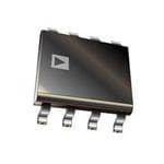
| 产品图片 |
|
| rohs | 符合RoHS无铅 / 符合限制有害物质指令(RoHS)规范要求 |
| 产品系列 | 放大器 IC,精密放大器,Analog Devices AD8597ARZ- |
| 数据手册 | |
| 产品型号 | AD8597ARZ |
| 产品培训模块 | http://www.digikey.cn/PTM/IndividualPTM.page?site=cn&lang=zhs&ptm=30008http://www.digikey.cn/PTM/IndividualPTM.page?site=cn&lang=zhs&ptm=26202 |
| 产品目录页面 | |
| 产品种类 | 精密放大器 |
| 供应商器件封装 | 8-SOIC N |
| 共模抑制比—最小值 | 135 dB |
| 关闭 | No |
| 包装 | 管件 |
| 压摆率 | 16 V/µs |
| 双重电源电压 | +/- 15 V |
| 可用增益调整 | 116 dB |
| 商标 | Analog Devices |
| 增益带宽生成 | 10 MHz |
| 增益带宽积 | 10MHz |
| 安装类型 | 表面贴装 |
| 安装风格 | SMD/SMT |
| 封装 | Tube |
| 封装/外壳 | 8-SOIC(0.154",3.90mm 宽) |
| 封装/箱体 | SOIC-8 |
| 工作温度 | -40°C ~ 125°C |
| 工作电源电压 | 15 V |
| 工厂包装数量 | 98 |
| 放大器类型 | 通用 |
| 最大双重电源电压 | 36 V |
| 最大工作温度 | + 125 C |
| 最小双重电源电压 | 10 V |
| 最小工作温度 | - 40 C |
| 标准包装 | 98 |
| 电压-电源,单/双 (±) | 9 V ~ 36 V, ±4.5 V ~ 18 V |
| 电压-输入失调 | 10µV |
| 电压增益dB | 116 dB |
| 电流-电源 | 5mA |
| 电流-输入偏置 | 25nA |
| 电流-输出/通道 | 52mA |
| 电源电压-最大 | 18 V |
| 电源电压-最小 | 5 V |
| 电源电流 | 5 mA |
| 电源类型 | Dual |
| 电路数 | 1 |
| 系列 | AD8597 |
| 视频文件 | http://www.digikey.cn/classic/video.aspx?PlayerID=1364138032001&width=640&height=505&videoID=2245193153001http://www.digikey.cn/classic/video.aspx?PlayerID=1364138032001&width=640&height=505&videoID=2245193159001 |
| 设计资源 | |
| 转换速度 | 16 V/us |
| 输入偏压电流—最大 | 300 nA |
| 输入电压范围—最大 | 12.5 V |
| 输入补偿电压 | 10 uV |
| 输出类型 | Rail to Rail Input |
| 通道数量 | 1 Channel |


PDF Datasheet 数据手册内容提取
Single and Dual, Ultralow Distortion, Ultralow Noise Op Amps Data Sheet AD8597/AD8599 FEATURES PIN CONFIGURATIONS Low noise: 1.1 nV/√Hz at 1 kHz NC 1 8 NC Low distortion: −120 dB THD at 1 kHz –IN 2 AD8597 7 V+ Input noise, 0.1 Hz to 10 Hz: <76 nV p-p +IN 3 TOP VIEW 6 OUT SWleidwe rbaaten:d 1w4i dVt/μhs: 10 MHz V– N4C (=N oNtO to C SOcNaNleE)CT5 NC 06274-060 Supply current: 4.8 mA/amp typical Figure 1. AD8597 8-Lead SOIC (R-8) Low offset voltage: 10 μV typical CMRR: 120 dB Unity-gain stable NC 1 8 NC ±15 V operation –IN 2 AD8597 7 V+ TOP VIEW APPLICATIONS +IN 3 (Not to Scale) 6 OUT V– 4 5 NC Professional audio preamplifiers ATE/precision testers NOTES 1.NC = NO CONNECT. IMmeadgicinagl/ psyhsytseimolso gical measurements 2 . IETTOX IP SVO –RS.EECDO PMAMDE BNED ECDO NTHNAECT TTEHDE 06274-061 Precision detectors/instruments Figure 2. AD8597 8-Lead LFCSP (CP-8-13) Precision data conversion OUT A 1 8 +V –IN A 2 AD8599 7 OUT B +IN– VA 34 (NToOt Pto V SIEcWale) 65 –+IINN BB 06274-054 Figure 3. AD8599 8-Lead SOIC (R-8) GENERAL DESCRIPTION The AD8597/AD8599 are very low noise, low distortion opera- The AD8597 is available in 8-lead SOIC and LFCSP packages, tional amplifiers ideal for use as preamplifiers. The low noise of while the AD8599 is available in an 8-lead SOIC package. They 1.1 nV/√Hz and low harmonic distortion of −120 dB (or better) are both specified over a −40°C to +125°C temperature range. at audio bandwidths give the AD8597/AD8599 the wide dynamic The AD8597 and AD8599 are members of a growing series of range necessary for preamplifiers in audio, medical, and instru- low noise op amps offered by Analog Devices, Inc. (see Table 1). mentation applications. The excellent slew rate of 14 V/μs and Table 1. Low Noise Op Amps 10 MHz gain bandwidth make them highly suitable for medical Package 0.9 nV 1.1 nV 1.8 nV 2.8 nV 3.8 nV applications. The low distortion and fast settling time make them ideal for buffering of high resolution data converters. Single AD797 AD8597 ADA4004-1 AD8675 AD8671 Dual AD8599 ADA4004-2 AD8676 AD8672 Quad ADA4004-4 AD8674 Rev. F Document Feedback Information furnished by Analog Devices is believed to be accurate and reliable. However, no responsibility is assumed by Analog Devices for its use, nor for any infringements of patents or other One Technology Way, P.O. Box 9106, Norwood, MA 02062-9106, U.S.A. rights of third parties that may result from its use. Specifications subject to change without notice. No license is granted by implication or otherwise under any patent or patent rights of Analog Devices. Tel: 781.329.4700 ©2007–2017 Analog Devices, Inc. All rights reserved. Trademarks and registered trademarks are the property of their respective owners. Technical Support www.analog.com
AD8597/AD8599 Data Sheet TABLE OF CONTENTS Features .............................................................................................. 1 ESD Caution...................................................................................5 Applications ....................................................................................... 1 Typical Performance Characteristics ..............................................6 Pin Configurations ........................................................................... 1 Functional Operation..................................................................... 15 General Description ......................................................................... 1 Input Voltage Range ................................................................... 15 Revision History ............................................................................... 2 Output Phase Reversal ............................................................... 15 Specifications ..................................................................................... 3 Noise and Source Impedance Considerations ........................... 15 Absolute Maximum Ratings ............................................................ 5 Outline Dimensions ....................................................................... 17 Thermal Resistance ...................................................................... 5 Ordering Guide .......................................................................... 17 Power Sequencing ........................................................................ 5 REVISION HISTORY 9/2017—Rev. E to Rev. F Changes to Specifications Section ................................................... 3 Changed CP-8-2 to CP-8-13 ........................................ Throughout Changes to Absolute Maximum Ratings Section .......................... 5 Updated Outline Dimensions ....................................................... 17 Changes to Typical Performance Characteristics Section ........... 6 Changes to Ordering Guide .......................................................... 17 Added Figure 12 and Figure 15 ....................................................... 7 Added Figure 18 and Figure 19 ....................................................... 8 10/2013—Rev. D to Rev. E Added Figure 30 and Figure 33 .................................................... 10 Change to Figure 15 Caption .......................................................... 7 Added Figure 34 to Figure 38 ....................................................... 11 Changes to Figure 23 and Figure 26 ............................................... 9 Added Figure 42 and Figure 45 .................................................... 12 Changes to Figure 30 and Figure 33 ............................................. 10 Added Figure 52, Figure 55, Figure 57 ........................................ 14 Changes to Figure 46 through Figure 50 ..................................... 13 Added Functional Operation Section .......................................... 15 Changes to Figure 53 and Figure 54 ............................................. 14 Added Figure 58 ............................................................................. 15 Updated Outline Dimensions ....................................................... 17 2/2013—Rev. C to Rev. D Changes to Ordering Guide .......................................................... 17 Changes to Figure 44 ...................................................................... 12 Changes to Figure 46 and Figure 49 ............................................. 13 4/2007—Rev. 0 to Rev. A Updated Layout ................................................................................. 5 12/2009—Rev. B to Rev. C Changes to Figure 45 Caption ...................................................... 12 Changes to Table 1 ............................................................................ 1 Added Figure 48 ............................................................................. 12 Changes to Figure 51 Caption ...................................................... 13 10/2008—Rev. A to Rev. B Added AD8597 ................................................................... Universal 2/2007—Revision 0: Initial Version Added LFCSP_VD ............................................................. Universal Added Table 1 .................................................................................... 1 Rev. F | Page 2 of 20
Data Sheet AD8597/AD8599 SPECIFICATIONS V = ±5 V, V = 0 V, V = 0 V, T = 25°C, unless otherwise specified. SY CM O A Table 2. Parameter Symbol Conditions Min Typ Max Unit INPUT CHARACTERISTICS Offset Voltage V 15 120 μV OS −40°C ≤ T ≤ +125°C 180 μV A Offset Voltage Drift ΔV /ΔT −40°C ≤ T ≤ +125°C 0.8 2.2 μV/°C OS A Input Bias Current I 40 210 nA B −40°C ≤ T ≤ +125°C 340 nA A Input Offset Current I 65 250 nA OS −40°C ≤ T ≤ +125°C 340 nA A Input Voltage Range IVR −2.0 +2.0 V Common-Mode Rejection Ratio CMRR −2.0 V ≤ V ≤ +2.0 V 120 135 dB CM −40°C ≤ T ≤ +125°C 105 dB A Large Signal Voltage Gain A R ≥ 600 Ω, V = −11 V to +11 V 105 110 dB VO L O −40°C ≤ T ≤ +125°C 100 dB A Input Capacitance Differential Capacitance C 15.4 pF DIFF Common-Mode Capacitance C 5.5 pF CM OUTPUT CHARACTERISTICS Output Voltage High V R = 600 Ω 3.5 3.7 V OH L −40°C ≤ T ≤ +125°C 3.3 V A R = 2 kΩ 3.7 3.8 V L −40°C ≤ T ≤ +125°C 3.5 V A Output Voltage Low V R = 600 Ω −3.6 −3.4 V OL L −40°C ≤ T ≤ +125°C −3.3 V A R = 2 kΩ −3.7 −3.5 V L −40°C ≤ T ≤ +125°C −3.4 V A Output Short-Circuit Current I ±52 mA SC Closed-Loop Output Impedance Z At 1 MHz, A = 1 5 Ω OUT V POWER SUPPLY Power Supply Rejection Ratio PSRR V = ±18 V to ±4.5 V 120 140 dB SY −40°C ≤ T ≤ +125°C 118 dB A Supply Current per Amplifier I 4.8 5.5 mA SY −40°C ≤ T ≤ +125°C 6.5 mA A DYNAMIC PERFORMANCE Slew Rate SR A = −1, R = 2 kΩ 14 V/μs V L A = 1, R = 2 kΩ 14 V/μs V L Settling Time t To 0.01%, step = 10 V 2 μs S Gain Bandwidth Product GBP 10 MHz Phase Margin Φ 60 Degrees M NOISE PERFORMANCE Peak-to-Peak Noise e p-p 0.1 Hz to 10 Hz 76 nV p-p n Voltage Noise Density e f = 1 kHz 1.07 1.15 nV/√Hz n f = 10 Hz 1.5 nV/√Hz Correlated Current Noise f = 1 kHz 2.0 pA/√Hz f = 10 Hz 4.2 pA/√Hz Uncorrelated Current Noise f = 1 kHz 2.4 pA/√Hz f = 10 Hz 5.2 pA/√Hz Total Harmonic Distortion + Noise THD + N G = 1, R ≥ 1 kΩ, f = 1 kHz, V = 1 V −120 dB L RMS Channel Separation CS f = 10 kHz −120 dB Rev. F | Page 3 of 20
AD8597/AD8599 Data Sheet V = ±15 V, V = 0 V, V = 0 V, T = +25°C, unless otherwise specified. S CM O A Table 3. Parameter Symbol Conditions Min Typ Max Unit INPUT CHARACTERISTICS Offset Voltage V 10 120 μV OS −40°C ≤ T ≤ +125°C 180 μV A Offset Voltage Drift ΔV /ΔT −40°C ≤ T ≤ +125°C 0.8 2.2 μV/°C OS A Input Bias Current I 25 200 nA B −40°C ≤ T ≤ +125°C 300 nA A Input Offset Current I 50 200 nA OS −40°C ≤ T ≤ +125°C 300 nA A Input Voltage Range IVR −12.5 +12.5 V Common-Mode Rejection Ratio CMRR −12.5 V ≤ V ≤ +12.5 V 120 135 dB CM −40°C ≤ T ≤ +125°C 115 dB A Large Signal Voltage Gain A R ≥ 600 Ω, V = −11 V to +11 V 110 116 dB VO L O −40°C ≤ T ≤ +125°C 106 dB A Input Capacitance Differential Capacitance C 12.1 pF DIFF Common-Mode Capacitance C 5.1 pF CM OUTPUT CHARACTERISTICS Output Voltage High V R = 600 Ω 13.1 13.4 V OH L −40°C ≤ T ≤ +125°C 12.8 V A R = 2 kΩ 13.5 13.7 V L −40°C ≤ T ≤ +125°C 13.2 V A Output Voltage Low V R = 600 Ω −13.2 −12.9 V OL L −40°C ≤ T ≤ +125°C −12.8 V A R = 2 kΩ −13.5 −13.4 V L −40°C ≤ T ≤ +125°C −13.3 V A Output Short-Circuit Current I ±52 mA SC Closed-Loop Output Impedance Z At 1 MHz, A = 1 5 Ω OUT V POWER SUPPLY Power Supply Rejection Ratio PSRR V = ±18 V to ±4.5 V 120 140 dB SY −40°C ≤ T ≤ +125°C 118 dB A Supply Current per Amplifier I 5.0 5.7 mA SY −40°C ≤ T ≤ +125°C 6.75 mA A DYNAMIC PERFORMANCE Slew Rate SR A = −1, R = 2 kΩ 16 V/μs V L A = 1, R = 2 kΩ 15 V/μs V L Settling Time t To 0.01%, step = 10 V 2 μs s Gain Bandwidth Product GBP 10 MHz Phase Margin Φ 65 Degrees M NOISE PERFORMANCE Peak-to-Peak Noise e p-p 0.1 Hz to 10 Hz 76 nV p-p n Voltage Noise Density e f = 1 kHz 1.07 1.15 nV/√Hz n f = 10 Hz 1.5 nV/√Hz Correlated Current Noise f = 1 kHz 1.9 pA/√Hz f = 10 Hz 4.3 pA/√Hz Uncorrelated Current Noise f = 1 kHz 2.3 pA/√Hz f = 10 Hz 5.3 pA/√Hz Total Harmonic Distortion + Noise THD + N G = 1, R ≥ 1 kΩ, f = 1 kHz, V = 3 V −120 dB L RMS Channel Separation CS f = 10 kHz −120 dB Rev. F | Page 4 of 20
Data Sheet AD8597/AD8599 ABSOLUTE MAXIMUM RATINGS THERMAL RESISTANCE Table 4. θ is specified with the device soldered on a circuit board with Parameter Rating JA its exposed paddle soldered to a pad (if applicable) on a 4-layer Supply Voltage ±18 V JEDEC standard PCB with zero air flow. Input Voltage −V ≤ V ≤ +V IN Differential Input Voltage1 ±1 V Table 5. Output Short-Circuit to GND Indefinite Package Type θ θ Unit JA JC Storage Temperature Range −65°C to +150°C 8-Lead LFCSP (CP-8-13) 78 20 °C/W Operating Temperature Range −40°C to +125°C 8-Lead SOIC (R-8) (AD8597) 140 39 °C/W Lead Temperature Range (Soldering 60 sec) 300°C 8-Lead SOIC (R-8) (AD8599) 120 36 °C/W Junction Temperature 150°C POWER SEQUENCING 1 If the differential input voltage exceeds 1 V, limit the current to 5 mA. Stresses at or above those listed under Absolute Maximum Apply the op amp supplies simultaneously. The op amp supplies Ratings may cause permanent damage to the product. This is a must be stable before any input signals are applied. In any case, stress rating only; functional operation of the product at these the input current must be limited to 5 mA. or any other conditions above those indicated in the operational section of this specification is not implied. Operation beyond ESD CAUTION the maximum operating conditions for extended periods may affect product reliability. Rev. F | Page 5 of 20
AD8597/AD8599 Data Sheet TYPICAL PERFORMANCE CHARACTERISTICS T = 25°C, unless otherwise noted. A 70 70 AD8599 AD8599 MEAN = 8.23 MEAN = 7.91 60 STDEV = 24.47 60 STDEV = 21.89 MIN = –72.62 MIN = –63.02 MAX = 62.09 MAX = 57.5 ERS 50 VSY = ±5V ERS 50 VSY = ±15V FI FI LI LI P 40 P 40 M M A A F F R O 30 R O 30 E E B B M M U 20 U 20 N N 10 10 0–75–65–55–45–35–25–15V–O5S (µ5V)15 25 35 45 55 65 75 06274-001 0–75–65–55–45–35–25–15V–O5S (µ5V)15 25 35 45 55 65 75 06274-002 Figure 4. Input Offset Voltage Distribution Figure 7. Input Offset Voltage Distribution 60 45 AD8599 AD8599 MEAN = 0.346 MEAN = 0.765 40 STDEV = 0.218 STDEV = 0.234 50 MIN = 0.010 MIN = 0.338 MAX = 1.155 35 MAX = 1.709 S S FIER 40 VSY = ±5V FIER 30 VSY = ±15V LI LI MP MP 25 F A 30 F A O O 20 R R E E MB 20 MB 15 U U N N 10 10 5 0 0 0.2 0.4 0.6 0.8 1.0TCV1.O2S (1µ.V4) 1.6 1.8 2.0 2.2 2.4 06274-004 0 0 0.2 0.4 0.6 0.8 1.0TCV1.O2S (1µ.V4) 1.6 1.8 2.0 2.2 2.4 06274-007 Figure 5. TCVOS Distribution, −40°C ≤ TA ≤ +125°C Figure 8. TCVOS Distribution, −40°C ≤ TA ≤ +125°C 60 60 AD8599 AD8599 MEAN = 0.461 MEAN = 0.342 STDEV = 0.245 STDEV = 0.221 50 MIN = 0.026 50 MIN = 0.013 S MAX = 1.26 S MAX = 1.239 FIER 40 VSY = ±5V FIER 40 VSY = ±15V LI LI P P M M F A 30 F A 30 O O R R E E MB 20 MB 20 U U N N 10 10 0 0 0.2 0.4 0.6 0.8 1.0TCV1.O2S (1µ.V4) 1.6 1.8 2.0 2.2 2.4 06274-006 0 0 0.2 0.4 0.6 0.8 1.0TCV1.O2S (1µ.V4) 1.6 1.8 2.0 2.2 2.4 06274-005 Figure 6. TCVOS Distribution, −40°C ≤ TA ≤ +85°C Figure 9. TCVOS Distribution, −40°C ≤ TA ≤ +85°C Rev. F | Page 6 of 20
Data Sheet AD8597/AD8599 100 100 AD8599 AD8599 75 VSY = ±5V 75 VSY = ±15V 50 50 25 25 V) V) (µS 0 (µS 0 O O V V –25 –25 –50 –50 –75 –75 –100 –100 –5.0 –2.5 VCM0 (V) 2.5 5.0 06274-009 –15 –10 –5 VCM0 (V) 5 10 15 06274-010 Figure 10. Offset Voltage vs. VCM Figure 13. Offset Voltage vs. VCM 350 350 AD8599 AD8599 300 VSY = ±5V 300 VSY = ±15V 250 VCM = 0V 250 VCM = 0V 200 200 150 150 A)100 A) 100 n n (B 50 (B 50 I I 0 0 –50 –50 –100 –100 –150 –150 –200–50 –25 0 TEM2P5ERATUR50E (°C) 75 100 125 06274-011 –200–50 –25 0 TEM2P5ERATUR50E (°C) 75 100 125 06274-012 Figure 11. Input Bias Current vs. Temperature Figure 14. Input Bias Current vs. Temperature 50 350 AD8597 40 AD8597 300 VSY = ±15V 250 30 200 150 20 TA = –40°C 100 V (µV)OS –11000 ±15V I (nA)B –55000 TA = +25°C TA = +85°C –100 TA = +125°C –20 –150 ±5V –200 –30 –250 ––4500 06274-062 ––330500 06274-063 –50 –25 0 25 50 75 100 125 150 –12 –10 –8 –6 –4 –2 0 2 4 6 8 10 12 TEMPERATURE (°C) VCM (V) Figure 12. Input Offset Voltage vs. Temperature Figure 15. Input Bias Current vs. Common-Mode Voltage (VCM) Over Temperature Rev. F | Page 7 of 20
AD8597/AD8599 Data Sheet 80 150 AD8597 AD8599 70 100 60 50 50 (nA)OS 40 IOS @ VSY = ±5V I (nA)B 0 ±15V ±5V I 30 –50 20 IOS @ VSY = ±15V –100 100–50 –25 0 TEM2P5ERATUR50E (°C) 75 100 125 06274-013 –150–50 –25 0 TEMP25ERATUR5E0 (°C) 75 100 12506274-065 Figure 16. Input Offset Current vs. Temperature Figure 19. Input Offset Current vs. Temperature 114 120 AD8599 AD8599 VSY = ±5V VSY = ±15V 112 118 RL = 2kΩ, VO = ±11V 110 RL = 2kΩ, VO = ±2V 116 B) 108 B) d d (O RL = 600Ω, VO = ±2V (O RL = 600Ω, VO = ±11V AV 106 AV 114 104 112 102 100–50 –25 0 T2E5MPERA50TURE (7°5C) 100 125 150 06274-015 110–50 –25 0 T2E5MPERA50TURE (7°5C) 100 125 150 06274-016 Figure 17. Large Signal Voltage Gain vs. Temperature Figure 20. Large Signal Voltage Gain vs. Temperature 8 AD8597 350 300 AD8599 7 TA = +125°C 250 VSY = ±15V TA = –40°C 6 TA = +85°C 200 150 5 TA = +25°C 100 I (mA)SY 4 TA = –40°C I (nA)B –55000 TTAA == ++8255°°CC 3 –100 2 –150 TA = +125°C –200 100 2 4 6 8 10 12 14 1V6S1Y8 (V2)0 22 24 26 28 30 32 34 3606274-064 –––323550000–12 –10 –8 –6 –4 –2VCM0 (V)2 4 6 8 10 12 06274-014 Figure 18. Supply Current vs. Supply Voltage Figure 21. Input Bias Current vs. VCM Rev. F | Page 8 of 20
Data Sheet AD8597/AD8599 80 80 AD8599 AD8599 60 VSY = ±5V 60 VSY = ±15V ISINK ISINK 40 40 A) A) m m T ( 20 T ( 20 N N E E R R R 0 R 0 U U C C T T U–20 U–20 P P T T U U O–40 O–40 ISOURCE ISOURCE –60 –60 –80–50 –25 0 T2E5MPERA50TURE (7°5C) 100 125 150 06274-017 –80–50 –25 0 T2E5MPERA50TURE (7°5C) 100 125 150 06274-018 Figure 22. ISC vs. Temperature Figure 25. ISC vs. Temperature V – V) (V)OUTS 10 AVSDY8 5=9 ±95V – V) (V)OUTS 10 AVSDY8 5=9 ±915V OUTPUT DROPOUT VOLTAGE ( 1 ISIISNOKURCE OUTPUT DROPOUT VOLTAGE (V 1 ISIOSUINRKCE 0.01.001 0.01 0.1 IL (mA) 1 10 100 06274-021 0.10.001 0.01 0.1 IL (mA) 1 10 100 06274-022 Figure 23. Output Dropout Voltage vs. Current Load Figure 26. Output Dropout Voltage vs. Current Load 2.5 2.5 AD8599 AD8599 VSY = ±5V VSY = ±15V 2.0 2.0 VCC – VOH@ RL = 600Ω V) 1.5 V) 1.5 (H VCC – VOH@ RL = 600Ω (H O O V V V – CC 1.0 VCC – VOH@ RL = 2kΩ V – CC1.0 VCC – VOH@ RL = 2kΩ 0.5 0.5 0–50 –25 0 T2E5MPERA50TURE (7°C5) 100 125 150 06274-027 0–50 –25 0 T2E5MPERA50TURE (7°C5) 100 125 150 06274-029 Figure 24. Output Saturation Voltage vs. Temperature Figure 27. Output Saturation Voltage vs. Temperature Rev. F | Page 9 of 20
AD8597/AD8599 Data Sheet 0 0 AD8599 AD8599 VSY = ±5V VSY = ±15V –0.5 –0.5 V) –1.0 V) –1.0 (OL VEE – VOL@ RL = 2kΩ (OL – V – V VEE – VOL@ RL = 2kΩ EE–1.5 EE–1.5 V VEE – VOL@ RL = 600Ω V –2.0 –2.0 VEE – VOL@ RL = 600Ω –2.5–50 –25 0 T2E5MPERA50TURE (7°C5) 100 125 150 06274-028 –2.5–50 –25 0 T2E5MPERA50TURE (7°5C) 100 125 150 06274-030 Figure 28. Output Saturation Voltage vs. Temperature Figure 31. Output Saturation Voltage vs. Temperature –13.0 15.0 VOL@ RL = 600Ω AD8599 14.8 VSY = ±15V 14.6 –13.5 14.4 VOL@ RL = 2kΩ 14.2 V) V) (L –14.0 (H14.0 O O V V 13.8 VOH@ RL = 2kΩ 13.6 –14.5 13.4 VOH@ RL = 600Ω AD8599 13.2 VSY = ±15V –15.0–50 0 TEMPERA50TURE (°C) 100 150 06274-032 13.0–50 0 TEMPERA50TURE (°C) 100 150 06274-031 Figure 29. Output Voltage Low vs. Temperature Figure 32. Output Voltage High vs. Temperature 100 100 120 100 80 80 100 80 60 60 80 60 40 CL = 20pF 40 grees) 60 40 grees) GAIN (dB)–22000 –02200 MARGIN (De GAIN (dB) 24000 CL = 20pF –02200 MARGIN (De CL = 200pF SE SE –40 –40 A –20 –40 A H H –60 –60 P –40 CL = 200pF –60 P AD8597 –1–0800 RVSLY = = 2 k±Ω5V ––81000 ––8600 AVRSDLY 8= 5= 29 ±k7Ω15V ––81000 10 100 FREQUENC1Yk (kHz) 10k 50k 06274-066 1 10 FRE10Q0UENCY (kH1zk) 10k 50k 06274-067 Figure 30. Gain and Phase vs. Frequency Figure 33. Gain and Phase vs. Frequency Rev. F | Page 10 of 20
Data Sheet AD8597/AD8599 50 50 40 40 AV = 100 AV = 100 30 30 20 20 AV = 10 AV = 10 dB) 10 dB) 10 N ( N ( AI 0 AI 0 G AV = 1 G AV = 1 –10 –10 –20 –20 AD8597 AD8597 ––3400 RVSLY = = 2 k±Ω5V 06274-068 ––3400 VRSLY = = 2 k±Ω15V 06274-071 1 10 100 1k 10k 50k 1 10 100 1k 10k 50k FREQUENCY (kHz) FREQUENCY (kHz) Figure 34. Closed-Loop Gain vs. Frequency Figure 37. Closed-Loop Gain vs. Frequency 100 100 AV = –100 AV = –100 10 10 AV = –10 AV = –10 Ω) AV = +1 Ω) AV = +1 (UT 1 (UT 1 O O Z Z 0.1 0.1 0.01 AVSDY8 5=9 ±75V 06274-069 0.01 AVSDY8 5=9 ±715V 06274-072 10 100 1k 10k 100k 10 100 1k 10k 100k FREQUENCY (kHz) FREQUENCY (kHz) Figure 35. Closed-Loop Output Impedance vs. Frequency Figure 38. Closed-Loop Output Impedance vs. Frequency 110 120 AD8599 100 ±5V ≤ VSY ≤ ±15V 100 PSRR+ (dB) 90 PSRR– (dB) 80 80 RR (dB) 70 R (dB) 60 M 60 AD8597 R C VSY = ±5V, ±15V PS 40 50 20 40 3200 06274-070 0 1 10 FREQUE1N00CY (kHz) 1k 10k –20100 1k F1R0EkQUENCY1 (0H0zk) 1M 10M 06274-038 Figure 36. Common-Mode Rejection Ratio vs. Frequency Figure 39. Power Supply Rejection Ratio vs. Frequency Rev. F | Page 11 of 20
AD8597/AD8599 Data Sheet 90 600 AD8599 AD8599 MEAN = 1.30 MEAN = 1.07 80 STDEV = 0.09 STDEV = 0.02 500 MIN = 1.1 MIN = 1.05 MPLIFIERS 765000 M±5AVX ≤ = V 1S.Y5 ≤ ±15V MPLIFIERS400 M±5AVX ≤ = V 1S.Y1 5≤ ±15V OF A 40 OF A300 R R MBE 30 MBE200 U U N N 20 100 10 01.0 1.1 1.2VOL1T.3AGE1 .N4OIS1.E5 DE1N.6SITY1 .(7nV/ 1 H.8z) 1.9 2.0 06274-039 00.95 0.98 1V.0O1LTA1G.0E4 NO1I.S0E7 DE1N.S10ITY 1(n.1V3/ H1z.)16 1.19 06274-040 Figure 40. Voltage Noise Density at 10 Hz Figure 43. Voltage Noise Density at 1 kHz 100 100 AD8599 AD8599 ±5V ≤ VSY ≤ ±15V ±5V ≤ VSY ≤ ±15V VOLTAGE NOISE DENSITY (nV/ Hz) 101 CURRTENT NOISE DENSITY (pA/ Hz) 10 0.11 10FREQUENCY (Hz)100 1k 06274-041 11 10 FREQU1E0N0CY (Hz) 1k 10k 06274-042 Figure 41. Voltage Noise Density vs. Frequency Figure 44. Current Noise Density vs. Frequency 1 1 0.1 0.1 %) RL = 600Ω %) N ( N ( + 0.01 + 0.01 D D H AD8597 H AD8597 T VSY = ±5V T VSY = ±15V AV = +1 AV = +1 0.001 0.001 RL = 600Ω 0.0001 RL = 100kΩ 06274-073 0.0001 RL = 100kΩ 06274-074 0.001 0.01 0.1 1 10 0.001 0.01 0.1 1 10 V rms (V) V rms (V) Figure 42. THD + N vs. Amplitude Figure 45. THD + N vs. Amplitude Rev. F | Page 12 of 20
Data Sheet AD8597/AD8599 0.1 0.1 AD8599 AD8599 VSY = ±15V VSY = ±15V VIN = 3V rms VIN = 3V rms VIN = 5V rms VIN = 7V rms 0.01 0.01 %) %) N ( N ( + + D D H H T T 0.001 RL = 600Ω 0.001 RL = 2kΩ 0.000110 100 FREQUE1NkCY (Hz) 10k 100k 06274-043 0.000110 100 FREQUE1NkCY (Hz) 10k 100k 06274-044 Figure 46. THD + N vs. Frequency Figure 49. THD + N vs. Frequency 20 20 AD8599 VSY = ±15V AD8599 VSY = ±15V 15 VIN = 20V p-p 15 VIN = 20V p-p AV = 1 AV = –1 RF = 1kΩ RF = 2kΩ 10 RL = 2kΩ 10 RS = 2kΩ E (V) 5 E (V) 5 CL = 0pF D D TU 0 TU 0 LI LI P P AM–5 AM–5 –10 –10 –15 –15 –2–08.6 –4.6 –0.6 3.4 7.4TIM11E. 4(µs1)5.4 19.4 23.4 27.4 31.4 06274-047 –2–08.6 –4.6 –0.6 3.4 7.4TIM1E1. 4(µs1)5.4 19.4 23.4 27.4 31.4 06274-048 Figure 47. Large Signal Response Figure 50. Large Signal Response 80 45 AD8599 AD8599 60 40 ±5V ≤ VSY ≤ ±15V AV = 1 35 RL = 10kΩ 40 E (mV) 20 OT (%)3205 D O U 0 H LIT RS20 P E M–20 V A O15 –40 VVSINY == 1±0105mVV, ± p5-Vp 10 AV = 1 –60 EXTERNAL CL = 100pF 5 EXTERNAL RL = 10kΩ –8–0800 –400 0 400 800TIM12E0 (0ns1)600 2000 2400 2800 3200 06274-046 010 CAPACIT1A00NCE (pF) 1k 06274-049 Figure 48. Small Signal Response Figure 51. Overshoot vs. Capacitance Rev. F | Page 13 of 20
AD8597/AD8599 Data Sheet 45 45 AD8597 AD8597 40 VSY = ±5V 40 VSY = ±15V 35 35 OS– %) 30 %) 30 OT ( 25 OT ( 25 O O H H RS 20 RS 20 VE OS– VE O 15 O 15 OS+ 10 10 OS+ 50 06247-077 50 06247-078 10 100 1k 10 100 1k CAPACITANCE (pF) CAPACITANCE (pF) Figure 52. Overshoot vs. Capacitive Load Figure 55. Overshoot vs. Capacitive Load 0 15.0 AD8599 10kΩ AD8599 –20 AVSVY = = 1 ±0105V VCC VCC 1kΩ RL = 1kΩ dB) –40 12.5 N ( 10V p-p VEE 2kΩ 2kΩ VEE TIO –60 CH A CCHH BC,, RA CH D A) SEPA –80 (mSY10.0 VSY = ±15V EL –100 I N AN VSY = ±5V H –120 7.5 C –140 VIN = 10V p-p VIN = 20V p-p –160100 1k FREQU1E0NkCY (Hz) 100k 1M 06274-050 5.0–50 –25 0 TEMP25ERATUR50E (°C) 75 100 125 06274-020 Figure 53. Channel Separation vs. Frequency Figure 56. Supply Current vs. Temperature 400 6.0 AD8599 AD8597 ±5V ≤ VSY ≤ ±15V 200 5.5 nV) VSY = ±15V E ( A) PLITUD 0 I (mSY 5.0 VSY = ±5V M A –200 4.5 –4000 1 2 3 T4IME (S5econd6s) 7 8 9 10 06274-053 4.0–40 –25 –10 5 T2E0MPE35RATU50RE (°6C5) 80 95 110 12506274-075 Figure 54. Peak-to-Peak Noise Figure 57. Supply Current vs. Temperature Rev. F | Page 14 of 20
Data Sheet AD8597/AD8599 FUNCTIONAL OPERATION INPUT VOLTAGE RANGE The AD8597/AD8599 amplifiers are carefully designed to prevent any output phase reversal if both inputs are maintained within The AD8597/AD8599 are not rail-to-rail input amplifiers; the specified input voltage range. If one or both inputs exceed therefore, care is required to ensure that both inputs do not the input voltage range but remain within the supply rails, the exceed the input voltage range. Under normal negative feedback op amp specifications, such as CMRR, are not guaranteed, but operating conditions, the amplifier corrects its output to ensure the output remains close to the correct value. that the two inputs are at the same voltage. However, if either input exceeds the input voltage range, the loop opens and large NOISE AND SOURCE IMPEDANCE CONSIDERATIONS currents begin to flow through the ESD protection diodes in the The AD8597/AD8599 ultralow voltage noise of 1.1 nV/√Hz is amplifier. achieved with special input transistors running at high collector These diodes are connected between the inputs and each supply current. Therefore, it is important to consider the total input- rail to protect the input transistors against an electrostatic discharge referred noise (e total), which includes contributions from N event and they are normally reverse-biased. However, if the voltage noise (e ), current noise (i ), and resistor noise N N input voltage exceeds the supply voltage, these ESD diodes can (√4 kTR). S become forward-biased. Without current limiting, excessive e total = [e 2 + 4 kTR + (i × R)2]1/2 (1) N N S N S amounts of current may flow through these diodes, causing where R is the total input source resistance. permanent damage to the device. If inputs are subject to over- S voltage, insert appropriate series resistors to limit the diode This equation is plotted for the AD8597/AD8599 in Figure 58. current to less than 5 mA maximum. Because optimum dc performance is obtained with matched source resistances, this case is considered even though it is clear The input stage has two diodes between the input pins to protect from Equation 1 that eliminating the balancing source resistance the differential pair. Under high slew rate conditions, when the lowers the total noise by reducing the total R by a factor of 2. op amp is connected as a voltage follower, the diodes may become S forward-biased and the source may try to drive the output. At a very low source resistance (RS < 50 Ω), the voltage noise of the Place a small resistor in the feedback loop and in the noninverting amplifier dominates. As source resistance increases, the Johnson input. The noise of a 100 Ω resistor at room temperature is noise of RS dominates until a higher resistance of RS > 2 kΩ is ~1.25 nV/√Hz, which is higher than the AD8597/AD8599. achieved; the current noise component is larger than the Thus, there is a tradeoff between noise performance and resistor noise. protection. If possible, place limiting earlier in the signal path. 100 For further details, see the Amplifier Input Protection… Friend or Foe? article at http://www.analog.com/amplifier_input. Binepcuatu csea poafc tihtaen lcaer gme atrya sneseimsto rrast uhseer dh itgoh a.c Thoie tvaek elo awd vnaonistaeg, eth oef V/ Hz) 10 n the low noise performance, impedance around the op amp must E ( S TOTAL NOISE be low, less than 500 Ω. Under these conditions, the pole from NOI RESISTOR NOISE the input capacitance must be greater than 50 MHz, which does AL ONLY not affect the signal bandwidth. OT 1 T OUTPUT PHASE REVERSAL Ocoumtpmuot np-hmasoed ree vvoelrtsaagl eo rcacnugres iisn e sxocmeeed eadm. pAlsif tiheres c womhemno tnh-em inopduet 0.1 06274-076 10 100 1k 10k voltage is moved outside the input voltage range, the outputs of SOURCE RESISTANCE (Ω) these amplifiers can suddenly jump in the opposite direction to Figure 58. Noise vs. Source Resistance the supply rail. This is the result of the differential input pair shutting down that causes a radical shifting of internal voltages that results in the erratic output behavior. Rev. F | Page 15 of 20
AD8597/AD8599 Data Sheet The AD8597/AD8599 are the optimum choice for low noise general noise theory with extensive calculations, see the performance if the source resistance is kept < 1 kΩ. At higher AN-358 Application Note, Noise and Operational Amplifier values of source resistance, optimum performance with respect Circuits. A good selection table for low noise op amps can to only noise is obtained with other amplifiers from Analog be found in AN-940 Application Note, Low Noise Amplifier Devices. Both voltage noise and current noise must be consi- Selection Guide for Optimal Noise Performance. An interesting dered. For more information on avoiding noise from grounding note on using one section of a monolithic dual to phase compen- problems and inadequate bypassing, see the AN-345 Application sate the other section is in the AN-107 Application Note, Active Note, Grounding for Low- and High-Frequency Circuits. For Feedback Improves Amplifier Phase Accuracy. V+ 7 Q36 R18 R19 D1 D31 R31 D2 D34 6 2 INVINEPRUTTING – Q18 Q19 VB C1 R1 OUTPUT Q19 Q20 D39 D41 D3 D40 D42 R32 3 NONINVERTING INPUT + Q32 D2 V–4 Q27 Q28 06247-079 Figure 59. Simplified Schematic Rev. F | Page 16 of 20
Data Sheet AD8597/AD8599 OUTLINE DIMENSIONS 5.00(0.1968) 4.80(0.1890) 8 5 4.00(0.1574) 6.20(0.2441) 3.80(0.1497) 1 4 5.80(0.2284) 1.27(0.0500) 0.50(0.0196) BSC 1.75(0.0688) 0.25(0.0099) 45° 0.25(0.0098) 1.35(0.0532) 8° 0.10(0.0040) 0° COPLANARITY 0.51(0.0201) 0.10 SEATING 0.31(0.0122) 0.25(0.0098) 10..2470((00..00510507)) PLANE 0.17(0.0067) COMPLIANTTOJEDECSTANDARDSMS-012-AA C(RINOEFNPEATRRREOENNLCLTEIHNEOGSNDELISYM)AEANNRDSEIAORRNOESUNANORDETEDAIN-POMPFRIFLOLMPIMIRLELIATIMTEEERTFSEO;RIRNECUQHSUEDIVIINMAELDENENSSTIIOGSNNFS.OR 012407-A Figure 60. 8-Lead Standard Small Outline Package [SOIC_N] Narrow Body (R-8) Dimensions shown in millimeters and (inches) DETAIL A 1.84 (JEDEC 95) 3.10 1.74 3.00 SQ 2.90 0.50 1.64 BSC 5 8 PIN 1 INDEX EXPOSED 1.55 AREA PAD 1.45 0.50 1.35 0.40 0.30 4 1 TOP VIEW BOTTOM VIEW PIN 1 INDICATOR AREA OPTIONS (SEE DETAIL A) 0.80 FOR PROPER CONNECTION OF 0.75 SIDE VIEW 0.05 MAX TTHHEE EPXINP COOSNEDFI GPAUDR,A RTEIOFNE RA NTOD 0.70 0.02 NOM FUNCTION DESCRIPTIONS COPLANARITY SECTION OF THIS DATA SHEET. SEATING 0.30 0.08 PLANE 0.25 0.203 REF PKG-003886 0C.O20MPLIANTTOJEDEC STANDARDS MO-229-WEED-4 02-10-2017-A Figure 61. 8-Lead Lead Frame Chip Scale Package [LFCSP] 3 mm × 3 mm Body and 0.75 mm Package Height (CP-8-13) Dimensions shown in millimeters ORDERING GUIDE Model1 Temperature Range Package Description Package Option Branding AD8597ACPZ-R2 −40°C to +125°C 8-Lead Lead Frame Chip Scale Package [LFCSP] CP-8-13 A22 AD8597ACPZ-REEL −40°C to +125°C 8-Lead Lead Frame Chip Scale Package [LFCSP] CP-8-13 A22 AD8597ACPZ-REEL7 −40°C to +125°C 8-Lead Lead Frame Chip Scale Package [LFCSP] CP-8-13 A22 AD8597ARZ −40°C to +125°C 8-Lead Standard Small Outline Package [SOIC_N] R-8 AD8597ARZ-REEL −40°C to +125°C 8-Lead Standard Small Outline Package [SOIC_N] R-8 AD8597ARZ-REEL7 −40°C to +125°C 8-Lead Standard Small Outline Package [SOIC_N] R-8 AD8599ARZ −40°C to +125°C 8-Lead Standard Small Outline Package [SOIC_N] R-8 AD8599ARZ-REEL −40°C to +125°C 8-Lead Standard Small Outline Package [SOIC_N] R-8 AD8599ARZ-REEL7 −40°C to +125°C 8-Lead Standard Small Outline Package [SOIC_N] R-8 1 Z = RoHS Complaint Part. Rev. F | Page 17 of 20
AD8597/AD8599 Data Sheet NOTES Rev. F | Page 18 of 20
Data Sheet AD8597/AD8599 NOTES Rev. F | Page 19 of 20
AD8597/AD8599 Data Sheet NOTES ©2007–2017 Analog Devices, Inc. All rights reserved. Trademarks and registered trademarks are the property of their respective owners. D06274-0-9/17(F) Rev. F | Page 20 of 20
Mouser Electronics Authorized Distributor Click to View Pricing, Inventory, Delivery & Lifecycle Information: A nalog Devices Inc.: AD8597ARZ AD8597ACPZ-R2 AD8597ACPZ-REEL AD8597ACPZ-REEL7 AD8597ARZ-REEL AD8597ARZ- REEL7