ICGOO在线商城 > 集成电路(IC) > 线性 - 放大器 - 仪表,运算放大器,缓冲器放大器 > AD847ARZ-REEL7
 Datasheet下载
- 型号: AD847ARZ-REEL7
- 制造商: Analog
- 库位|库存: xxxx|xxxx
- 要求:
| 数量阶梯 | 香港交货 | 国内含税 |
| +xxxx | $xxxx | ¥xxxx |
查看当月历史价格
查看今年历史价格
AD847ARZ-REEL7产品简介:
ICGOO电子元器件商城为您提供AD847ARZ-REEL7由Analog设计生产,在icgoo商城现货销售,并且可以通过原厂、代理商等渠道进行代购。 AD847ARZ-REEL7价格参考。AnalogAD847ARZ-REEL7封装/规格:线性 - 放大器 - 仪表,运算放大器,缓冲器放大器, 通用 放大器 1 电路 8-SOIC。您可以下载AD847ARZ-REEL7参考资料、Datasheet数据手册功能说明书,资料中有AD847ARZ-REEL7 详细功能的应用电路图电压和使用方法及教程。
AD847ARZ-REEL7 是由 Analog Devices Inc. 生产的线性放大器,具体分类为仪表、运算放大器和缓冲器放大器。这款器件具有高精度、低噪声和高速度等特性,适用于多种精密测量和信号处理应用场景。

1. 医疗设备:在医疗领域,AD847ARZ-REEL7 可用于心电图(ECG)、脑电图(EEG)和其他生物医学信号的放大和处理。其低噪声特性和高增益带宽积使其能够准确捕捉微弱的生理信号,确保诊断结果的准确性。

2. 工业自动化:该放大器可以用于工业控制系统中的传感器信号调理。例如,在温度、压力或位移传感器中,AD847ARZ-REEL7 能够将传感器输出的微弱信号放大到适合后续处理的水平,同时保持信号的完整性,提高系统的稳定性和可靠性。

3. 测试与测量仪器:在高精度测试设备中,如示波器、频谱分析仪等,AD847ARZ-REEL7 的高速性能和低失真特性使其成为理想的信号放大元件。它可以快速响应输入信号的变化,提供清晰、准确的测量结果。

4. 音频处理:对于高质量音频设备,AD847ARZ-REEL7 的低失真和低噪声特性非常适合用于前置放大器,确保音频信号在传输过程中不被污染,保留原始音质。

5. 通信系统:在无线通信和有线通信设备中,AD847ARZ-REEL7 可以作为中频放大器,用于放大和处理射频信号。其宽带宽和高线性度有助于提高通信系统的信噪比和传输质量。

6. 消费电子:在一些高端消费电子产品中,如专业级摄影机、摄像机等,AD847ARZ-REEL7 可以用于图像传感器信号的放大和处理,确保图像质量和动态范围的最大化。

总之,AD847ARZ-REEL7 凭借其卓越的性能和可靠性,广泛应用于需要高精度信号处理的各种场合,是众多精密测量和控制系统中的理想选择。
| 参数 | 数值 |
| -3db带宽 | - |
| 产品目录 | 集成电路 (IC) |
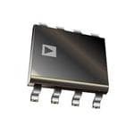
| 描述 | IC OPAMP GP 50MHZ 8SOIC |
| 产品分类 | Linear - Amplifiers - Instrumentation, OP Amps, Buffer Amps |
| 品牌 | Analog Devices Inc |
| 数据手册 | |
| 产品图片 |
|
| 产品型号 | AD847ARZ-REEL7 |
| rohs | 无铅 / 符合限制有害物质指令(RoHS)规范要求 |
| 产品系列 | - |
| 产品培训模块 | http://www.digikey.cn/PTM/IndividualPTM.page?site=cn&lang=zhs&ptm=30008http://www.digikey.cn/PTM/IndividualPTM.page?site=cn&lang=zhs&ptm=26202 |
| 供应商器件封装 | 8-SOIC |
| 包装 | 剪切带 (CT) |
| 压摆率 | 300 V/µs |
| 增益带宽积 | 50MHz |
| 安装类型 | 表面贴装 |
| 封装/外壳 | 8-SOIC(0.154",3.90mm 宽) |
| 工作温度 | -40°C ~ 85°C |
| 放大器类型 | 通用 |
| 标准包装 | 1 |
| 电压-电源,单/双 (±) | ±4.5 V ~ 18 V |
| 电压-输入失调 | 500µV |
| 电流-电源 | 5.3mA |
| 电流-输入偏置 | 3.3µA |
| 电流-输出/通道 | 32mA |
| 电路数 | 1 |
| 视频文件 | http://www.digikey.cn/classic/video.aspx?PlayerID=1364138032001&width=640&height=505&videoID=2245193153001http://www.digikey.cn/classic/video.aspx?PlayerID=1364138032001&width=640&height=505&videoID=2245193159001 |
| 输出类型 | - |


- 商务部:美国ITC正式对集成电路等产品启动337调查
- 曝三星4nm工艺存在良率问题 高通将骁龙8 Gen1或转产台积电
- 太阳诱电将投资9.5亿元在常州建新厂生产MLCC 预计2023年完工
- 英特尔发布欧洲新工厂建设计划 深化IDM 2.0 战略
- 台积电先进制程称霸业界 有大客户加持明年业绩稳了
- 达到5530亿美元!SIA预计今年全球半导体销售额将创下新高
- 英特尔拟将自动驾驶子公司Mobileye上市 估值或超500亿美元
- 三星加码芯片和SET,合并消费电子和移动部门,撤换高东真等 CEO
- 三星电子宣布重大人事变动 还合并消费电子和移动部门
- 海关总署:前11个月进口集成电路产品价值2.52万亿元 增长14.8%


PDF Datasheet 数据手册内容提取
a High Speed, Low Power Monolithic Op Amp AD847 FEATURES CONNECTION DIAGRAM Superior Performance High Unity Gain BW: 50 MHz Plastic DIP (N), Low Supply Current: 5.3 mA Small Outline (R) and High Slew Rate: 300 V/(cid:109)s Cerdip (Q) Packages Excellent Video Specifications 0.04% Differential Gain (NTSC and PAL) 0.19(cid:56) Differential Phase (NTSC and PAL) Drives Any Capacitive Load Fast Settling Time to 0.1% (10 V Step): 65 ns Excellent DC Performance High Open-Loop Gain 5.5 V/mV (R = 1 k(cid:86)) LOAD Low Input Offset Voltage: 0.5 mV Specified for (cid:54)5 V and (cid:54)15 V Operation Available in a Wide Variety of Options Plastic DIP and SOIC Packages Cerdip Package Die Form specifications which include an open-loop gain of 3500 V/V MIL-STD-883B Processing (500 W load) and low input offset voltage of 0.5 mV. Common- Tape & Reel (EIA-481A Standard) mode rejection is a minimum of 78 dB. Output voltage swing is Dual Version Available: AD827 (8 Lead) – 3 V into loads as low as 150 W . Analog Devices also offers Enhanced Replacement for LM6361 over 30 other high speed amplifiers from the low noise AD829 Replacement for HA2544, HA2520/2/5 and EL2020 (1.7 nV/(cid:214) Hz) to the ultimate video amplifier, the AD811, which APPLICATIONS features 0.01% differential gain and 0.01(cid:176) differential phase. Video Instrumentation Imaging Equipment APPLICATION HIGHLIGHTS Copiers, Fax, Scanners, Cameras 1. As a buffer the AD847 offers a full-power bandwidth of High Speed Cable Driver 12.7 MHz (5 V p-p with – 5 V supplies) making it outstand- High Speed DAC and Flash ADC Buffers ing as an input buffer for flash A/D converters. 2. The low power and small outline package of the AD847 make it very well suited for high density applications such as PRODUCT DESCRIPTION multiple pole active filters. The AD847 represents a breakthrough in high speed amplifiers offering superior ac & dc performance and low power, all at low 3. The AD847 is internally compensated for unity gain opera- cost. The excellent dc performance is demonstrated by its – 5 V tion and remains stable when driving any capacitive load. 6 A m – 5.5 T N E R R CU 5 T N E C S E4.5 UI Q 4 0 5 10 15 20 SUPPLY VOLTAGE – – Volts Quiescent Current vs. Supply Voltage AD847 Driving Capacitive Loads REV.F Information furnished by Analog Devices is believed to be accurate and reliable. However, no responsibility is assumed by Analog Devices for its use, nor for any infringements of patents or other rights of third parties which may result from its use. No license is granted by implication or One Technology Way, P.O. Box 9106, Norwood, MA 02062-9106, U.S.A. otherwise under any patent or patent rights of Analog Devices. Tel: 617/329-4700 Fax: 617/326-8703
AD847–SPECIFICATIONS (@ T = +25(cid:56)C, unless otherwise noted) A Model AD847J AD847AR Conditions V Min Typ Max Min Typ Max Units S INPUT OFFSET VOLTAGE1 – 5 V 0.5 1 0.5 1 mV T to T 3.5 4 mV MIN MAX Offset Drift 15 15 m V/(cid:176) C INPUT BIAS CURRENT – 5 V, – 15 V 3.3 6.6 3.3 6.6 m A T to T 7.2 10 m A MIN MAX INPUT OFFSET CURRENT – 5 V, – 15 V 50 300 50 300 nA T to T 400 500 nA MIN MAX Offset Current Drift 0.3 0.3 nA/(cid:176) C OPEN-LOOP GAIN V = – 2.5 V – 5 V OUT R = 500 W 2 3.5 2 3.5 V/mV LOAD T to T 1 1 V/mV MIN MAX R = 150 W 1.6 1.6 V/mV LOAD V = – 10 V – 15 V OUT R = 1 kW 3 5.5 3 5.5 V/mV LOAD T to T 1.5 1.5 V/mV MIN MAX DYNAMIC PERFORMANCE Unity Gain Bandwidth – 5 V 35 35 MHz – 15 V 50 50 MHz Full Power Bandwidth2 V = 5 V p-p OUT R = 500 W , – 5 V 12.7 12.7 MHz LOAD V = 20 V p-p, OUT R = 1 kW – 15 V 4.7 4.7 MHz LOAD Slew Rate3 R = 1 kW – 5 V 200 200 V/m s LOAD – 15 V 225 300 225 300 V/m s Settling Time to 0.1%, R = 250 W –2.5 V to +2.5 V – 5 V 65 65 ns LOAD 10 V Step, A = –1 – 15 V 65 65 ns V to 0.01%, R = 250 W –2.5 V to +2.5 V – 5 V 140 140 ns LOAD 10 V Step, A = –1 – 15 V 120 120 ns V Phase Margin C = 10 pF – 15 V LOAD R = 1 kW 50 50 Degree LOAD Differential Gain f » 4.4 MHz, R = 1 kW – 15 V 0.04 0.04 % LOAD Differential Phase f » 4.4 MHz, R = 1 kW – 15 V 0.19 0.19 Degree LOAD COMMON-MODE REJECTION V = – 2.5 V – 5 V 78 95 78 95 dB CM V = – 12 V – 15 V 78 95 78 95 dB CM T to T 75 75 dB MIN MAX POWER SUPPLY REJECTION V = – 5 V to – 15 V 75 86 75 86 dB S T to T 72 72 dB MIN MAX INPUT VOLTAGE NOISE f = 10 kHz – 15 V 15 15 nV/(cid:214) Hz INPUT CURRENT NOISE f = 10 kHz – 15 V 1.5 1.5 pA/(cid:214) Hz INPUT COMMON-MODE VOLTAGE RANGE – 5 V +4.3 +4.3 V –3.4 –3.4 V – 15 V +14.3 +14.3 V –13.4 –13.4 V OUTPUT VOLTAGE SWING R = 500 W – 5 V 3.0 3.6 3.0 3.6 – V LOAD R = 150 W – 5 V 2.5 3 2.5 3 – V LOAD R = 1 kW – 15 V 12 12 – V LOAD R = 500 W – 15 V 10 10 – V LOAD Short-Circuit Current – 15 V 32 32 mA INPUT RESISTANCE 300 300 kW INPUT CAPACITANCE 1.5 1.5 pF OUTPUT RESISTANCE Open Loop 15 15 W POWER SUPPLY Operating Range (cid:54)4.5 (cid:54)18 (cid:54)4.5 (cid:54)18 V Quiescent Current – 5 V 4.8 6.0 4.8 6.0 mA T to T 7.3 7.3 mA MIN MAX – 15 V 5.3 6.3 5.3 6.3 mA T to T 7.6 7.6 mA MIN MAX NOTES lInput Offset Voltage Specifications are guaranteed after 5 minutes at T = +25(cid:176)C. A 2Full Power Bandwidth = Slew Rate/2 p V . PEAK 3Slew Rate is measured on rising edge. All min and max specifications are guaranteed. Specifications in boldface are 100% tested at final electrical test. Specifications subject to change without notice. –2– REV. F
AD847 Model AD847AQ AD847S Conditions V Min Typ Max Min Typ Max Units S INPUT OFFSET VOLTAGE1 – 5 V 0.5 1 0.5 1 mV T to T 4 4 mV MIN MAX Offset Drift 15 15 m V/(cid:176) C INPUT BIAS CURRENT – 5 V, – 15 V 3.3 5 3.3 5 m A T to T 7.5 7.5 m A MIN MAX INPUT OFFSET CURRENT – 5 V, – 15 V 50 300 50 300 nA T to T 400 400 nA MIN MAX Offset Current Drift 0.3 0.3 nA/(cid:176) C OPEN-LOOP GAIN V = – 2.5 V – 5 V OUT R = 500 W 2 3.5 2 3.5 V/mV LOAD T to T 1 1 V/mV MIN MAX R = 150 W 1.6 1.6 V/mV LOAD V = = – 10 V – 15 V OUT R = 1 kW 3 5.5 3 5.5 V/mV LOAD T to T 1.5 1.5 V/mV MIN MAX DYNAMIC PERFORMANCE Unity Gain Bandwidth – 5 V 35 35 MHz – 15 V 50 50 MHz Full Power Bandwidth2 V = 5 V p-p OUT R = 500 W , – 5 V 12.7 12.7 MHz LOAD V = 20 V p-p, OUT R = 1 kW – 15 V 4.7 4.7 MHz LOAD Slew Rate3 R = 1 kW – 5 V 200 200 V/m s LOAD – 15 V 225 300 225 300 V/m s Settling Time to 0.1%, R = 250 W –2.5 V to +2.5 V – 5 V 65 65 ns LOAD 10 V Step, A = –1 – 15 V 65 65 ns V to 0.01%, R = 250 W –2.5 V to +2.5 V – 5 V 140 140 ns LOAD 10 V Step, A = –1 – 15 V 120 120 ns V Phase Margin C = 10 pF – 15 V LOAD R = 1 kW 50 50 Degree LOAD Differential Gain f » 4.4 MHz, R = 1 kW – 15 V 0.04 0.04 % LOAD Differential Phase f » 4.4 MHz, R = 1 kW – 15 V 0.19 0.19 Degree LOAD COMMON-MODE REJECTION V = – 2.5 V – 5 V 80 95 80 95 dB CM V = – 12 V – 15 V 80 95 80 95 dB CM T to T 75 75 dB MIN MAX POWER SUPPLY REJECTION V = – 5 V to – 15 V 75 86 75 86 dB S T to T 72 72 dB MIN MAX INPUT VOLTAGE NOISE f = 10 kHz – 15 V 15 15 nV/(cid:214) Hz INPUT CURRENT NOISE f = 10 kHz – 15 V 1.5 1.5 pA/(cid:214) Hz INPUT COMMON-MODE VOLTAGE RANGE – 5 V +4.3 +4.3 V –3.4 –3.4 V – 15 V +14.3 +14.3 V –13.4 –13.4 V OUTPUT VOLTAGE SWING R = 500 W – 5 V 3.0 3.6 3.0 3.6 – V LOAD R = 150 W – 5 V 2.5 3 2.5 3 – V LOAD R = 1 kW – 15 V 12 12 – V LOAD R = 500 W – 15 V 10 10 – V LOAD Short-Circuit Current – 15 V 32 32 mA INPUT RESISTANCE 300 300 kW INPUT CAPACITANCE 1.5 1.5 pF OUTPUT RESISTANCE Open Loop 15 15 W POWER SUPPLY Operating Range (cid:54)4.5 (cid:54)18 (cid:54)4.5 (cid:54)18 V Quiescent Current – 5 V 4.8 5.7 4.8 5.7 mA T to T 7.0 7.8 mA MIN MAX – 15 V 5.3 6.3 5.3 6.3 mA T to T 7.6 8.4 mA MIN MAX REV. F –3–
AD847 ABSOLUTE MAXIMUM RATINGS1 ESD SUSCEPTIBILITY Supply Voltage . . . . . . . . . . . . . . . . . . . . . . . . . . . . . . . .– 18 V ESD (electrostatic discharge) sensitive device. Electrostatic Internal Power Dissipation2 charges as high as 4000 volts, which readily accumulate on the Plastic (N) . . . . . . . . . . . . . . . . . . . . . . . . . . . . . . 1.2 Watts human body and on test equipment, can discharge without de- Small Outline (R) . . . . . . . . . . . . . . . . . . . . . . . . . 0.8 Watts tection. Although the AD847 features proprietary ESD protec- Cerdip (Q) . . . . . . . . . . . . . . . . . . . . . . . . . . . . . . 1.1 Watts tion circuitry, permanent damage may still occur on these Input Voltage . . . . . . . . . . . . . . . . . . . . . . . . . . . . . . . . . . .– V devices if they are subjected to high energy electrostatic dis- S Differential Input Voltage . . . . . . . . . . . . . . . . . . . . . . . .– 6 V charges. Therefore, proper ESD precautions are recommended Storage Temperature Range (Q) . . . . . . . . . –65(cid:176) C to +150(cid:176) C to avoid any performance degradation or loss of functionality. (N, R) . . . . . . . . . . . . . . . . . . . . . . . . . . . –65(cid:176) C to +125(cid:176) C Junction Temperature . . . . . . . . . . . . . . . . . . . . . . . . . .175(cid:176) C Lead Temperature Range (Soldering 60 sec) . . . . . . . +300(cid:176) C NOTES 1Stresses above those listed under “Absolute Maximum Ratings” may cause permanent damage to the device. This is a stress rating only, and functional operation of the device at these or any other conditions above those indicated in the operational section of this specification is not implied. Exposure to absolute maximum rating conditions for extended periods may affect device reliability. 2Mini-DIP Package: q = 100(cid:176)C/Watt; q = 33(cid:176)C/Watt JA JC Cerdip Package: q = 110(cid:176)C/Watt; q = 30(cid:176)C/Watt JA JC Small Outline Package: q = 155(cid:176)C/Watt; q = 33(cid:176) C/Watt JA JC METALIZATION PHOTOGRAPH Contact factory for latest dimensions. Dimensions shown in inches and (mm). ORDERING GUIDE Temperature Package Package Models* Range – (cid:56)C Description Option AD847JN 0 to +70 Plastic N-8 AD847JR 0 to +70 SOIC R-8 AD847AQ –40 to +85 Cerdip Q-8 AD847AR –40 to +85 SOIC R-8 AD847SQ –55 to +125 Cerdip Q-8 AD847SQ/883B –55 to +125 Cerdip Q-8 5962-8964701PA –55 to +125 Cerdip Q-8 *AD847 also available in J and S grade chips, and AD847JR and AD847AR are available *in tape and reel. –4– REV. F
AD847 Typical Characteristics (@ +25(cid:56)C and V = (cid:54)15 V, unless otherwise noted) S 20 20 s Volt olts –GE – 15 G – V 15 MODE RAN 10 +VIN TAGE SWIN 10 +VOUT MMON- –VIN UT VOL –VOUT CO 5 TP 5 PUT OU R L O A D = 500W N I 0 0 0 5 10 15 20 0 5 10 15 20 SUPPLY VOLTAGE – – Volts SUPPLY VOLTAGE – – Volts Figure 1.Input Common-Mode Range vs. Supply Voltage Figure 2.Output Voltage Swing vs. Supply Voltage 30 6 p p- 25 olts mA5.5 G – V 20 NT – N E WI – 15 V SUPPLIES RR E S 15 CU 5 AG NT UTPUT VOLT 105 – 5V SUPPLIES QUIESCE4.5 O 0 4 10 100 1k 10k 0 5 10 15 20 LOAD RESISTANCE – W SUPPLY VOLTAGE – – Volts Figure 3.Output Voltage Swing vs. Load Resistance Figure 4.Quiescent Current vs. Supply Voltage 5 100 A 10 mS CURRENT – 4 VS = – 5V WMPEDANCE – 1 T BIA 3 PUT I U T P U N O 0.1 I 2 0.01 –60 –40 –20 0 20 40 60 80 100 120 140 10k 100k 1M 10M 100M TEMPERATURE – (cid:176)C FREQUENCY – Hz Figure 5.Input Bias Current vs. Temperature Figure 6.Output Impedance vs. Frequency REV. F –5–
AD847–Typical Characteristics (@ +25(cid:56)C and V = (cid:54)15 V, unless otherwise noted) S 7 35 A m NT – mA 6 T LIMIT – 30 E N R E R R CU 5 UR 25 NT T C QUIESCE 4 T CIRCUI 20 VS = – 5V HOR S 3 15 –60 –40 –20 0 20 40 60 80 100 120 140 –60 –40 –20 0 20 40 60 80 100 120 140 TEMPERATURE – (cid:176)C AMBIENT TEMPERATURE – (cid:176)C Figure 7.Quiescent Current vs. Temperature Figure 8.Short-Circuit Current Limit vs. Temperature 52 100 +100(cid:176) Hz 80 +80(cid:176) NDWIDTH – M 51 GAIN – dB 60 – 5V5 0S0UWP PLLOIAEDS 1–k1W5V L OSUAPDPLIES +60(cid:176) – DEGREES N BA 50 OOP 40 +40(cid:176) RGIN – GAI EN -L 20 +20(cid:176) E MA UNITY 49 OP 0 0 PHAS 48 –20 –60 –40 –20 0 20 40 60 80 100 120 140 100 1k 10k 100k 1M 10M 100M TEMPERATURE – (cid:176)C FREQUENCY – Hz Figure 9.Gain Bandwidth Product vs. Temperature Figure 10.Open-Loop Gain and Phase Margin vs. Frequency 80 100 75 VS = – 15V +SUPPLY dB 80 – B N P GAIN – d 6750 VS = – 5V REJECTIO 60 OO LY –SUPPLY OPEN-L 60 R SUPP 40 E W 55 O 20 P 50 0 10 100 1k 10k 1k 10k 100k 1M 10M 100M LOAD RESISTANCE – W FREQUENCY – Hz Figure 11.Open-Loop Gain vs. Load Resistance Figure 12.Power Supply Rejection vs. Frequency –6– REV. F
AD847 100 30 25 80 p VC M = – 1V p-p s p– olt 20 V R – dB 60 TAGE – 15 R L = 1kW M L C 40 VO UT 10 P T U 20 O 5 0 0 1k 10k 100k 1M 10M 100M 1M 10M 100M FREQUENCY – Hz INPUT FREQUENCY – Hz Figure 13.Common-Mode Rejection vs. Frequency Figure 14.Large Signal Frequency Response 10 –70 8 –80 V 6 dB 3V RMS –TO 4 N – R L =1kW 0 O –90 M TI 2ND HARMONIC O 2 R R 1% 0.1% O F T NG 0 DIS–100 SWI –2 1% 0.1% NIC PUT –4 RMO–110 T A 3RD HARMONIC U H O –6 –120 –8 –10 –130 0 20 40 60 80 100 120 140 160 100 1k 10k 100k SETTLING TIME – ns FREQUENCY – Hz Figure 15.Output Swing and Error vs. Settling Time Figure 16.Harmonic Distortion vs. Frequency 50 450 Hz 40 400 V/ SE – n 30 m– V/s350 OI E TAGE N 20 EW RAT300 L L O S250 V T U P 10 N 200 I 0 150 10 100 1k 10k 100k 1M 10M –60 –40 –20 0 20 40 60 80 100 120 140 FREQUENCY – Hz TEMPERATURE – (cid:176)C Figure 17.Input Voltage Noise Spectral Density Figure 18.Slew Rate vs. Temperature REV. F –7–
AD847 Figure 19.Inverting Amplifier Configuration Figure 19a.Inverter Large Figure 19b.Inverter Small Signal Pulse Response Signal Pulse Response Figure 20.Noninverting Amplifier Configuration Figure 20a.Noninverting Figure 20b.Noninverting Large Signal Pulse Response Small Signal Pulse Response –8– REV. F
AD847 OFFSET NULLING +VS The input offset voltage of the AD847 is very low for a high speed op amp, but if additional nulling is required, the circuit shown in Figure 21 can be used. CF OUTPUT –IN +IN Figure 21.Offset Nulling –VS NULL 1 NULL 8 INPUT CONSIDERATIONS An input resistor (R in Figure 20) is required in circuits where Figure 22.AD847 Simplified Schematic IN the input to the AD847 will be subjected to transient or con- tinuous overload voltages exceeding the – 6 V maximum differ- GROUNDING AND BYPASSING ential limit. This resistor provides protection for the input In designing practical circuits with the AD847, the user must transistors by limiting the maximum current that can be forced remember that whenever high frequencies are involved, some into their bases. special precautions are in order. Circuits must be built with short interconnect leads. A large ground plane should be used For high performance circuits it is recommended that a resistor whenever possible to provide a low resistance, low inductance (R in Figures 19 and 20) be used to reduce bias current errors B circuit path, as well as minimizing the effects of high frequency by matching the impedance at each input. The offset voltage er- coupling. Sockets should be avoided because the increased ror will be reduced by more than an order of magnitude. interlead capacitance can degrade bandwidth. THEORY OF OPERATION Feedback resistors should be of low enough value to assure that The AD847 is fabricated on Analog Devices’ proprietary the time constant formed with the capacitance at the amplifier complementary bipolar (CB) process which enables the con- summing junction will not limit the amplifier performance. struction of pnp and npn transistors with similar f s in the Resistor values of less than 5 kW are recommended. If a larger T 600 MHz to 800 MHz region. The AD847 circuit (Figure 22) resistor must be used, a small (<10 pF) feedback capacitor in includes an npn input stage followed by fast pnps in the folded parallel with the feedback resistor, R , may be used to compen- F cascode intermediate gain stage. The CB pnps are also used in sate for the input capacitances and optimize the dynamic perfor- the current amplifying output stage. The internal compensation mance of the amplifier. capacitance that makes the AD847 unity gain stable is provided Power supply leads should be bypassed to ground as close as by the junction capacitances of transistors in the gain stage. possible to the amplifier pins. Ceramic disc capacitors of The capacitor, C , in the output stage mitigates the effect of ca- 0.1 m F are recommended. F pacitive loads. At low frequencies and with low capacitive loads, the gain from the compensation node to the output is very close to unity. In this case C is bootstrapped and does not F contribute to the compensation capacitance of the part. As the capacitive load is increased, a pole is formed with the output impedance of the output stage. This reduces the gain, and therefore, C is incompletely bootstrapped. Some fraction of C F F contributes to the compensation capacitance, and the unity gain bandwidth falls. As the load capacitance is increased, the band- width continues to fall, and the amplifier remains stable. REV. F –9–
AD847 VIDEO LINE DRIVER Figure 24 shows the AD847 driving 100 pF and 1000 pF loads. The AD847 functions very well as a low cost, high speed line driver for either terminated or unterminated cables. Figure 23 shows the AD847 driving a doubly terminated cable in a fol- lower configuration. The termination resistor, R , (when equal to the cable’s charac- T teristic impedance) minimizes reflections from the far end of the cable. While operating from – 5 V supplies, the AD847 main- tains a typical slew rate of 200 V/m s, which means it can drive a – 1 V, 30 MHz signal into a terminated cable. +VS C7O5AW X 1R00INW 0.1 m F 75W Figure 24.AD847 Driving Capacitive Loads VIN COAX 75W AD847 7R5BWT 7R5TW VOUT FTLhAe S35H M AHDCz u InNiPtyU gTai nB UbaFnFdEwRidth of the AD847 makes it an excellent choice for buffering the input of high speed flash A/D 0.1 m F converters, such as the AD9048. 500W –VS Figure 25 shows the AD847 as a unity inverter for the input to the AD9048. C 500W C 0.1 SEE TABLE I –5.2V AD589 2k 10kW Figure 23.Video Line Driver 27 Table I. Video Line Driver Performance Chart 100 0.1 2N3906 AD741 Over- 5 1k 1k V * V C –3 dB B shoot IN SUPPLY C W 1.5kW 0.1m F 0 dB or – 500 mV Step – 15 20 pF 23 MHz 4% 00 ddBB oorr –– 550000 mmVV SStteepp –– 1155 105 p pFF 2113 MMHHzz 00%% (0VA TNOIAN L+P2OUVGT) 51.05WkW AD847 43W VINRB RT D(M1SB) 0 dB or – 500 mV Step – 5 20 pF 18 MHz 2% 0 dB or – 500 mV Step – 5 15 pF 16 MHz 0% AD9048 0 dB or – 500 mV Step – 5 0 pF 11 MHz 0% TTL D8 CONVERT CONVERT (LSB) SIGNAL *–3 dB bandwidth numbers are for the 0 dBm signal input. Overshoot numbers VEE VCC are the percent overshoot of the 1 volt step input. 0.1m F 0.1m F A back-termination resistor (R , also equal to the characteristic BT impedance of the cable) may be placed between the AD847 out- –5.2V +5.0V put and the cable input, in order to damp any reflected signals Figure 25.Flash ADC Input Buffer caused by a mismatch between R and the cable’s characteristic T impedance. This will result in a flatter frequency response, al- though this requires that the op amp supply – 2 V to the output in order to achieve a – 1 V swing at resistor R . T –10– REV. F
AD847 A High Speed, Three Op-Amp In-Amp The input amplifier (A1 and A2) is an AD827, which is a dual The circuit of Figure 26 lends itself well to CCD imaging and version of the AD847. This circuit has the optional flexibility of other video speed applications. It uses two high speed CB pro- both dc and ac trims for common-mode rejection, plus the abil- cess op-amps: Amplifier A3, the output amplifier, is an AD847. ity to adjust for minimum settling time. EACH AMPLIFIER PIN 7 AD847, +15V +VS PIN 8 AD827 10m F 0.1m F 1m F 0.1m F COMM 10m F 0.1m F 1m F 0.1m F PIN 4 –15V –VS AD847 & AD827 1/2 2–8pF AD827 SETTLING TIME –VIN 3 AC CMR ADJUST A1 1 INPUT FREQUENCY CMRR 2 2kW 1kW 100Hz 88.3dB 2kW 1kHz 87.4dB 2 VOUT 10kHz 86.2dB RG 2kW A3 6 11M00HkzHz 6477..41ddBB 1kW 3 AD847 RL 2kW 1.87kW 5pF 6 A2 7 DC CMR +VIN 5 1/2 ADJUST AD827 200W CIRCUIT GAIN = 2 0 0 0 W + 1 RG BANDWIDTH, SETTLING TIME AND TOTAL HARMONIC DISTORTION VS. GAIN THD + NOISE SMALL SETTLING BELOW INPUT CADJ SIGNAL TIME LEVEL GAIN RG (pF) BANDWIDTH TO 0.1% @ 10kHz 1 OPEN 2–8 16.1MHz 200ns 82dB 2 2kW 2–8 14.7MHz 200ns 82dB 10 226W 2–8 4.5MHz 370ns 81dB 100 20W 2–8 660kHz 2.5m s 71dB Figure 26. A High Speed In-Amp Circuit for Data Acquisition REV. F –11–
AD847 HIGH SPEED DAC BUFFER (10.24 V for a 1 kW resistor). Note that since the DAC gener- The wide bandwidth and fast settling time of the AD847 makes ates a positive current to ground, the voltage at the amplifier it a very good output buffer for high speed current-output D/A output will be negative. A 100 W series resistor between the converters like the AD668. As shown in Figure 27, the op amp noninverting amplifier input and ground minimizes the offset establishes a summing node at ground for the DAC output. The effects of op amp input bias currents. output voltage is determined by the amplifier’s feedback resistor +15V 92 10m F 9/ – TO ANALOG 10 0.1m F GROUND PLANE 1f– 9 1 MSB VCC 24 11 C 2 REFCOM 23 –1V NOMINAL 3 REFIN1 22 +REFERENCE INPUT 4 REFIN2 21 10k 1k 5 IOUT 20 DIGITAL AD668 100W ANALOG INPUTS 6 RLOAD 19 AD847 OUTPUT 7 ACOM 18 ANALOG GROUND PLANE ANALOG 8 LCOM 17 SUPPLY GROUND 9 IBPO 16 0.1m F 10m F 10 VEE 15 –15V 11 THCOM 14 100pF 12 LSB VTH 13 +5V 1kW Figure 27. High Speed DAC Buffer OUTLINE DIMENSIONS Dimensions shown in inches and (mm). Mini-DIP (N-8) Package Cerdip (Q-8) Package Small Outline (R-8) Package 0.005 (0.13) MIN 0.055 (1.40) MAX 0.150 (3.81) 8 5 0.25 PIN 1 (6.35) 0.31 8 5 8 5 1 4 (7.87) PIN 1 00..321200 ((75..8579)) 00..224248 ((65..2709)) 00..115570 ((33..9891)) PIN 1 0.39 (9.91) MAX 1 4 1 4 0.035±0.01 0.165±0.01 (0.89±0.25) 0.405 (10.29) MAX (4.19±0.25) 0.060 (1.52) 0.200 0.015 (0.38) 0.197 (5.01) (5.08) 0.189 (4.80) (03.M.101(2.0I80N5.)1486±±00..00083) (B02..S15C04) (0N0.O0.83M43) SP0(EL4.AA1.5N8T7±IE±N00G.0.736) 00..210205 M((53A..01X880)).023 (0.58) 0.100 0.070 (1.78) 0(M3.I1.N8510) 00..001004 ((00..2150)) 0(B1.0.S25C70) 00..001194 ((00..438600))..100924 ((22..5399)) D IN U.S.A. 0.30R E(7F.62) 0.014 (0.36) (B2.S5C4) 0.030 (0.76) SPLEAANTIENG 0C.H02A0M (F0.051) x0 4.159°0 (4.82) NTE 00..322900 ((87..1337)) 80°° 0.170 (4.32) 0.090 PRI (2.29) 10° 0.011±0.003 0° (0.28±0.08) 0.098 (0.2482) 0.030 (0.76) 15° 0.015 (0.38) 0.075 (0.1905) 0.018 (0.46) 0° 0.008 (0.20) 15(cid:176) 0(cid:176) All brand or product names mentioned are trademarks or registered trademarks of their respective holders. –12– REV. F
Mouser Electronics Authorized Distributor Click to View Pricing, Inventory, Delivery & Lifecycle Information: A nalog Devices Inc.: AD847AR AD847ARZ AD847JNZ AD847JRZ AD847SQ 5962-8964701PA AD847AQ AD847AR-REEL7 AD847ARZ-REEL AD847ARZ-REEL7 AD847JN AD847JR AD847JR-REEL AD847JR-REEL7 AD847JRZ-REEL AD847JRZ-REEL7 AD847SQ/883B