ICGOO在线商城 > 集成电路(IC) > 线性 - 放大器 - 仪表,运算放大器,缓冲器放大器 > AD823ARZ-R7
 Datasheet下载
- 型号: AD823ARZ-R7
- 制造商: Analog
- 库位|库存: xxxx|xxxx
- 要求:
| 数量阶梯 | 香港交货 | 国内含税 |
| +xxxx | $xxxx | ¥xxxx |
查看当月历史价格
查看今年历史价格
AD823ARZ-R7产品简介:
ICGOO电子元器件商城为您提供AD823ARZ-R7由Analog设计生产,在icgoo商城现货销售,并且可以通过原厂、代理商等渠道进行代购。 AD823ARZ-R7价格参考。AnalogAD823ARZ-R7封装/规格:线性 - 放大器 - 仪表,运算放大器,缓冲器放大器, J-FET Amplifier 2 Circuit Rail-to-Rail 8-SOIC。您可以下载AD823ARZ-R7参考资料、Datasheet数据手册功能说明书,资料中有AD823ARZ-R7 详细功能的应用电路图电压和使用方法及教程。
AD823ARZ-R7是Analog Devices Inc.生产的一款高性能双通道运算放大器,属于线性放大器类别,广泛应用于对信号精度和稳定性要求较高的场合。该器件具有高带宽、低噪声、低失真和高输出驱动能力等特点,适用于工业自动化、精密测量、医疗设备、测试与测量仪器以及音频处理系统等场景。

在工业控制中,AD823ARZ-R7常用于传感器信号调理,如压力、温度或应变片信号的放大与处理,其高共模抑制比和低温漂特性确保了在复杂电磁环境下的信号准确性。在医疗设备(如心电图仪、病人监护仪)中,它可有效放大微弱生物电信号,同时抑制干扰,保障信号清晰可靠。

此外,该运放也适用于有源滤波、电压跟随、缓冲级设计及数据采集系统前端电路,能够驱动容性负载并保持稳定,适合多级放大架构中的中间级或输出级。其小尺寸封装(SOIC-8)和卷带包装形式便于自动化贴装,适用于大批量生产的高可靠性电子设备。

综上,AD823ARZ-R7凭借优异的动态性能和稳定性,成为精密模拟信号处理领域的理想选择。
| 参数 | 数值 |
| -3db带宽 | 16MHz |
| 产品目录 | 集成电路 (IC)半导体 |
| 描述 | IC OPAMP JFET 16MHZ RRO 8SOIC精密放大器 17MHz RR FET Input Dual |
| 产品分类 | Linear - Amplifiers - Instrumentation, OP Amps, Buffer Amps集成电路 - IC |
| 品牌 | Analog Devices |
| 产品手册 | |
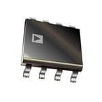
| 产品图片 |
|
| rohs | 符合RoHS无铅 / 符合限制有害物质指令(RoHS)规范要求 |
| 产品系列 | 放大器 IC,精密放大器,Analog Devices AD823ARZ-R7- |
| 数据手册 | |
| 产品型号 | AD823ARZ-R7 |
| 产品培训模块 | http://www.digikey.cn/PTM/IndividualPTM.page?site=cn&lang=zhs&ptm=30008http://www.digikey.cn/PTM/IndividualPTM.page?site=cn&lang=zhs&ptm=26202 |
| 产品种类 | 精密放大器 |
| 供应商器件封装 | 8-SOIC N |
| 共模抑制比—最小值 | 82 dB |
| 关闭 | No |
| 其它名称 | AD823ARZ-R7-ND |
| 包装 | 带卷 (TR) |
| 压摆率 | 25 V/µs |
| 双重电源电压 | +/- 3 V, +/- 5 V, +/- 9 V, +/- 12 V, +/- 15 V |
| 商标 | Analog Devices |
| 增益带宽生成 | 10 MHz |
| 增益带宽积 | - |
| 安装类型 | 表面贴装 |
| 安装风格 | SMD/SMT |
| 封装 | Reel |
| 封装/外壳 | 8-SOIC(0.154",3.90mm 宽) |
| 封装/箱体 | SOIC-8 |
| 工作温度 | -40°C ~ 85°C |
| 工作电源电压 | 3 V to 36 V |
| 工厂包装数量 | 750 |
| 放大器类型 | J-FET |
| 最大功率耗散 | 0.9 W |
| 最大双重电源电压 | +/- 18 V |
| 最大工作温度 | + 85 C |
| 最小双重电源电压 | +/- 1.5 V |
| 最小工作温度 | - 40 C |
| 标准包装 | 750 |
| 电压-电源,单/双 (±) | 3 V ~ 36 V, ±1.5 V ~ 18 V |
| 电压-输入失调 | 700µV |
| 电压增益dB | 93.06 dB |
| 电流-电源 | 7mA |
| 电流-输入偏置 | 5pA |
| 电流-输出/通道 | 17mA |
| 电源电压-最大 | 36 V |
| 电源电压-最小 | 3 V |
| 电源电流 | 7 mA |
| 电源类型 | Single, Dual |
| 电路数 | 2 |
| 系列 | AD823 |
| 视频文件 | http://www.digikey.cn/classic/video.aspx?PlayerID=1364138032001&width=640&height=505&videoID=2245193153001http://www.digikey.cn/classic/video.aspx?PlayerID=1364138032001&width=640&height=505&videoID=2245193159001 |
| 转换速度 | 25 V/us |
| 输入偏压电流—最大 | 30 pA |
| 输入电压范围—最大 | 13.8 V |
| 输入补偿电压 | 700 uV |
| 输出电流 | 17 mA |
| 输出类型 | Rail to Rail Output |
| 通道数量 | 2 Channel |


- 商务部:美国ITC正式对集成电路等产品启动337调查
- 曝三星4nm工艺存在良率问题 高通将骁龙8 Gen1或转产台积电
- 太阳诱电将投资9.5亿元在常州建新厂生产MLCC 预计2023年完工
- 英特尔发布欧洲新工厂建设计划 深化IDM 2.0 战略
- 台积电先进制程称霸业界 有大客户加持明年业绩稳了
- 达到5530亿美元!SIA预计今年全球半导体销售额将创下新高
- 英特尔拟将自动驾驶子公司Mobileye上市 估值或超500亿美元
- 三星加码芯片和SET,合并消费电子和移动部门,撤换高东真等 CEO
- 三星电子宣布重大人事变动 还合并消费电子和移动部门
- 海关总署:前11个月进口集成电路产品价值2.52万亿元 增长14.8%


PDF Datasheet 数据手册内容提取
Dual, 16 MHz, Rail-to-Rail FET Input Amplifier Data Sheet AD823 FEATURES CONNECTION DIAGRAM Single-supply operation OUT1 1 8 +VS Output swings rail-to-rail –IN1 2 7 OUT2 HigISnhinp lguoltae vd-os dultrpaivpgeley rcaanpgaeb eilxittye nfrdosm b 3el Vo wto g 3r6o uVn d +–INV1S 34 AD823 65 +–IINN22 00901-001 Figure 1. 8-Lead PDIP and SOIC Capacitive load drive of 500 pF, G = +1 Output current of 15 mA, 0.5 V from supplies Excellent ac performance on 2.6 mA/amplifier RL = 100kΩ −3 dB bandwidth of 16 MHz, G = +1 CL = 50pF 350 ns settling time to 0.01% (2 V step) 3V G+V =S +=1 +3V Slew rate of 22 V/µs Good dc performance 800 µV maximum input offset voltage 2 µV/°C offset voltage drift 25 pA maximum input bias current Low distortion: −108 dBc worst harmonic @ 20 kHz Low noise: 16 nV/√Hz @ 10 kHz GND No phase inversion with inputs to the supply rails APPLICATIONS 500mV 200µs 00901-002 Battery-powered precision instrumentation Figure 2. Output Swing, +VS = +3 V, G = +1 Photodiode preamps 2 Active filters +VS = +5V 1 G = +1 12-bit to 16-bit data acquisition systems Medical instrumentation 0 –1 GENERAL DESCRIPTION dB)–2 The AD823 is a dual precision, 16 MHz, JFET input op amp T ( U–3 P that can operate from a single supply of 3.0 V to 36 V or from T OU–4 dual supplies of ±1.5 V to ±18 V. It has true single-supply –5 capability with an input voltage range extending below ground –6 in single-supply mode. Output voltage swing extends to within 50 mV of each rail for I ≤ 100 µA, providing outstanding –7 OUT oAunt pouffts dety nvoamltaigce r aonf g8e0.0 µV maximum, an offset voltage drift of –81k 10k FRE1Q00UkENCY (Hz)1M 10M 00901-003 Figure 3. Small Signal Bandwidth, G = +1 2 µV/°C, input bias currents below 25 pA, and low input voltage noise provide dc precision with source impedances up to a This combination of ac and dc performance, plus the outstanding Gigaohm. It provides 16 MHz, −3 dB bandwidth, −108 dB THD load drive capability, results in an exceptionally versatile ampli- @ 20 kHz, and a 22 V/µs slew rate with a low supply current of fier for applications such as A/D drivers, high speed active 2.6 mA per amplifier. The AD823 drives up to 500 pF of direct filters, and other low voltage, high dynamic range systems. capacitive load as a follower and provides an output current of The AD823 is available over the industrial temperature range of 15 mA, 0.5 V from the supply rails. This allows the amplifier to −40°C to +85°C and is offered in both 8-lead PDIP and 8-lead handle a wide range of load conditions. SOIC packages. Rev. E Information furnished by Analog Devices is believed to be accurate and reliable. However, no responsibility is assumed by Analog Devices for its use, nor for any infringements of patents or other One Technology Way, P.O. Box 9106, Norwood, MA 02062-9106, U.S.A. rights of third parties that may result from its use. Specifications subject to change without notice. No license is granted by implication or otherwise under any patent or patent rights of Analog Devices. Tel: 781.329.4700 www.analog.com Trademarks and registered trademarks are the property of their respective owners. Fax: 781.461.3113 ©1995–2011 Analog Devices, Inc. All rights reserved.
AD823 Data Sheet TABLE OF CONTENTS Features .............................................................................................. 1 Typical Performance Characteristics ..............................................7 Applications ....................................................................................... 1 Theory of Operation ...................................................................... 13 General Description ......................................................................... 1 Output Impedance ..................................................................... 14 Connection Diagram ....................................................................... 1 Application Notes ........................................................................... 15 Revision History ............................................................................... 2 Input Characteristics .................................................................. 15 Specifications ..................................................................................... 3 Output Characteristics............................................................... 15 Absolute Maximum Ratings ............................................................ 6 Outline Dimensions ....................................................................... 18 Thermal Resistance ...................................................................... 6 Ordering Guide .......................................................................... 19 ESD Caution .................................................................................. 6 REVISION HISTORY 11/11—Rev. D to Rev. E Changes to Theory of Operation Section .................................... 13 Changes to Ordering Guide .......................................................... 19 6/10—Rev. C to Rev. D Changes to Figure 34 ...................................................................... 11 Changes to Figure 36 ...................................................................... 13 5/10—Rev. B to Rev. C Changes to Table 4 ............................................................................ 6 2/07—Rev. A to Rev. B Updated Format .................................................................. Universal Changes to DC Performance .......................................................... 5 Updated Outline Dimensions ....................................................... 18 Changes to Ordering Guide ......................................................... 19 5/04—Rev. 0 to Rev. A Changes to Specifications ................................................................ 2 Changes to Ordering Guide ......................................................... 17 Updated Outline Dimensions ....................................................... 17 5/95—Revision 0: Initial Version Rev. E | Page 2 of 20
Data Sheet AD823 SPECIFICATIONS At T = 25°C, +V = +5 V, R = 2 kΩ to 2.5 V, unless otherwise noted. A S L Table 1. Parameter Conditions Min Typ Max Unit DYNAMIC PERFORMANCE −3 dB Bandwidth, V ≤ 0.2 V p-p G = +1 12 16 MHz O Full Power Response V = 2 V p-p 3.5 MHz O Slew Rate G = −1, V = 4 V Step 14 22 V/µs O Settling Time to 0.1% G = −1, V = 2 V Step 320 ns O to 0.01% G = −1, V = 2 V Step 350 ns O NOISE/DISTORTION PERFORMANCE Input Voltage Noise f = 10 kHz 16 nV/√Hz Input Current Noise f = 1 kHz 1 fA/√Hz Harmonic Distortion R = 600 Ω to 2.5 V, V = 2 V p-p, f = 20 kHz −108 dBc L O Crosstalk f = 1 kHz R = 5 kΩ −105 dB L f = 1 MHz R = 5 kΩ −63 dB L DC PERFORMANCE Initial Offset 0.2 0.8 mV Maximum Offset Over temperature 0.3 2.0 mV Offset Drift 2 µV/°C Input Bias Current V = 0 V to 4 V 3 25 pA CM at T V = 0 V to 4 V 0.5 5 nA MAX CM Input Offset Current 2 20 pA at T 0.5 nA MAX Open-Loop Gain V = 0.2 V to 4 V, R = 2 kΩ 20 45 V/mV O L T to T 20 V/mV MIN MAX INPUT CHARACTERISTICS Input Common-Mode Voltage Range −0.2 to +3 −0.2 to +3.8 V Input Resistance 1013 Ω Input Capacitance 1.8 pF Common-Mode Rejection Ratio V = 0 V to 3 V 60 76 dB CM OUTPUT CHARACTERISTICS Output Voltage Swing I = ±100 µA 0.025 to 4.975 V L I = ±2 mA 0.08 to 4.92 V L I = ±10 mA 0.25 to 4.75 V L Output Current V = 0.5 V to 4.5 V 16 mA OUT Short-Circuit Current Sourcing to 2.5 V 40 mA Sinking to 2.5 V 30 mA Capacitive Load Drive G = +1 500 pF POWER SUPPLY Operating Range 3 36 V Quiescent Current T to T , total 5.2 5.6 mA MIN MAX Power Supply Rejection Ratio V = 5 V to 15 V, T to T 70 80 dB S MIN MAX Rev. E | Page 3 of 20
AD823 Data Sheet At T = 25°C, +V = +3.3 V, R = 2 kΩ to 1.65 V, unless otherwise noted. A S L Table 2. Parameter Conditions Min Typ Max Unit DYNAMIC PERFORMANCE −3 dB Bandwidth, V ≤ 0.2 V p-p G = +1 12 15 MHz O Full Power Response V = 2 V p-p 3.2 MHz O Slew Rate G = −1, V = 2 V Step 13 20 V/µs O Settling Time to 0.1% G = −1, V = 2 V Step 250 ns O to 0.01% G = −1, V = 2 V Step 300 ns O NOISE/DISTORTION PERFORMANCE Input Voltage Noise f = 10 kHz 16 nV/√Hz Input Current Noise f = 1 kHz 1 fA/√Hz Harmonic Distortion R = 100 Ω, V = 2 V p-p, f = 20 kHz −93 dBc L O Crosstalk f = 1 kHz R = 5 kΩ −105 dB L f = 1 MHz R = 5 kΩ −63 dB L DC PERFORMANCE Initial Offset 0.2 1.5 mV Maximum Offset Over temperature 0.5 2.5 mV Offset Drift 2 µV/°C Input Bias Current V = 0 V to 2 V 3 25 pA CM at T V = 0 V to 2 V 0.5 5 nA MAX CM Input Offset Current 2 20 pA at T 0.5 nA MAX Open-Loop Gain V = 0.2 V to 2 V, R = 2 kΩ 15 30 V/mV O L T to T 12 V/mV MIN MAX INPUT CHARACTERISTICS Input Common-Mode Voltage Range −0.2 to +1 −0.2 to +1.8 V Input Resistance 1013 Ω Input Capacitance 1.8 pF Common-Mode Rejection Ratio V = 0 V to 1 V 54 70 dB CM OUTPUT CHARACTERISTICS Output Voltage Swing I = ±100 µA 0.025 to 3.275 V L I = ±2 mA 0.08 to 3.22 V L I = ±10 mA 0.25 to 3.05 V L Output Current V = 0.5 V to 2.5 V 15 mA OUT Short-Circuit Current Sourcing to 1.5 V 40 mA Sinking to 1.5 V 30 mA Capacitive Load Drive G = +1 500 pF POWER SUPPLY Operating Range 3 36 V Quiescent Current T to T , total 5.0 5.7 mA MIN MAX Power Supply Rejection Ratio V = 3.3 V to 15 V, T to T 70 80 dB S MIN MAX Rev. E | Page 4 of 20
Data Sheet AD823 At T = 25°C, V = ±15 V, R = 2 kΩ to 0 V, unless otherwise noted. A S L Table 3. Parameter Conditions Min Typ Max Unit DYNAMIC PERFORMANCE −3 dB Bandwidth, V ≤ 0.2 V p-p G = +1 12 16 MHz O Full Power Response V = 2 V p-p 4 MHz O Slew Rate G = −1, V = 10 V Step 17 25 V/µs O Settling Time to 0.1% G = −1, V = 10 V Step 550 ns O to 0.01% G = −1, V = 10 V Step 650 ns O NOISE/DISTORTION PERFORMANCE Input Voltage Noise f = 10 kHz 16 nV/√Hz Input Current Noise f = 1 kHz 1 fA/√Hz Harmonic Distortion R = 600 Ω, V = 10 V p-p, f = 20 kHz −90 dBc L O Crosstalk f = 1 kHz R= 5 kΩ −105 dB L f = 1 MHz R= 5 kΩ −63 dB L DC PERFORMANCE Initial Offset 0.7 3.5 mV Maximum Offset Over temperature 1.0 7 mV Offset Drift 2 µV/°C Input Bias Current V = 0 V 5 30 pA CM V = −10 V 60 pA CM at T V = 0 V 0.5 5 nA MAX CM Input Offset Current 2 20 pA at T 0.5 nA MAX Open-Loop Gain V = +10 V to −10 V, R = 2 kΩ 30 60 V/mV O L T to T 30 V/mV MIN MAX INPUT CHARACTERISTICS Input Common-Mode Voltage Range −15.2 to +13 −15.2 to +13.8 V Input Resistance 1013 Ω Input Capacitance 1.8 pF Common-Mode Rejection Ratio V = −15 V to +13 V 66 82 dB CM OUTPUT CHARACTERISTICS Output Voltage Swing I = ±100 µA −14.95 to +14.95 V L I = ±2 mA −14.92 to +14.92 V L I = ±10 mA −14.75 to +14.75 V L Output Current V = −14.5 V to +14.5 V 17 mA OUT Short-Circuit Current Sourcing to 0 V 80 mA Sinking to 0 V 60 mA Capacitive Load Drive G = +1 500 pF POWER SUPPLY Operating Range 3 36 V Quiescent Current T to T , total 7.0 8.4 mA MIN MAX Power Supply Rejection Ratio V = 5 V to 15 V, T to T 70 80 dB S MIN MAX Rev. E | Page 5 of 20
AD823 Data Sheet ABSOLUTE MAXIMUM RATINGS THERMAL RESISTANCE Table 4. Parameter Rating θ is specified for the worst-case conditions, that is, a device JA Supply Voltage 36 V soldered in a circuit board for surface-mount packages. Internal Power Dissipation Specification is for device in free air. PDIP (N) 1.3 W SOIC (R) 0.9 W Table 5. Thermal Resistance Input Voltage (Common Mode) ±VS Package Type θJA Unit Differential Input Voltage ±VS 8-Lead PDIP 90 °C/W Output Short-Circuit Duration See Figure 4 8-Lead SOIC 160 °C/W Storage Temperature Range N, R −65°C to +125°C Operating Temperature Range −40°C to +85°C 2.0 Lead Temperature Range 300°C 8-LEAD PDIP TJ = 150°C (Soldering, 10 sec) W) Stresses above those listed under Absolute Maximum Ratings N ( O1.5 may cause permanent damage to the device. This is a stress ATI P rating only; functional operation of the device at these or any SI S DI other conditions above those indicated in the operational R 1.0 E section of this specification is not implied. Exposure to absolute W O maximum rating conditions for extended periods may affect UM P 8-LEAD SOIC device reliability. M0.5 XI A M 0–50–40 –30 –20A–1M0BIE0NT 1T0EM2P0ERA30TUR4E0 (°5C0) 60 70 80 90 00901-004 Figure 4. Maximum Power Dissipation vs. Temperature ESD CAUTION Rev. E | Page 6 of 20
Data Sheet AD823 TYPICAL PERFORMANCE CHARACTERISTICS 80 100 +VS = +5V +VS = +5V 314 UNITS 90 317 UNITS 70 σ = 40µV σ = 0.4pA 80 60 70 50 60 S S NIT40 NIT50 U U 40 30 30 20 20 10 10 0–200 –150 –10IN0PUT– 5O0FFSET0 VOLT5A0GE (µ1V0)0 150 200 00901-005 00 1 2 IN3PUT 4BIAS C5URRE6NT (p7A) 8 9 10 00901-008 Figure 5. Typical Distribution of Input Offset Voltage Figure 8. Typical Distribution of Input Bias Current 22 10000 +VS = +5V +VS = +5V 20 –55°CTO +125°C VCM = 0V 103 UNITS 18 1000 A) 16 p T ( 14 N E100 R TS12 UR NI C U10 S 8 T BIA 10 U 6 P N I 1 4 2 0–6 –5 –4IN–P3UT –O2FFS–1ET V0OLT1AGE 2DRIF3T (µV4/°C)5 6 7 00901-006 0.10 25 TEM5P0ERATURE 7(5°C) 100 125 00901-009 Figure 6. Typical Distribution of Input Offset Voltage Drift Figure 9. Input Bias Current vs. Temperature 3 1000 +VS = +5V VS= ±15V 2 A) 1 pA)100 T (p NT ( N E RE 0 RR R U U C 10 S C –1 AS A BI PUT BI –2 NPUT 1 N I I –3 –4–5 –4 –3 C–O2MMO–N1-MOD0E VO1LTAGE2 (V) 3 4 5 00901-007 0.1–16 –12 –8COMM–O4N-MO0DE VOL4TAGE (8V) 12 16 00901-010 Figure 7. Input Bias Current vs. Common-Mode Voltage Figure 10. Input Bias Current vs. Common-Mode Voltage Rev. E | Page 7 of 20
AD823 Data Sheet 110 95 VS = ±2.5V RL = 2kΩ 94 +VS = +5V 100 93 B) B) N (d N (d92 AI90 AI G G91 OP OP O O90 N-L80 N-L OPE OPE89 88 70 87 60100 1kLOAD RESIS1T0AkNCE (Ω) 100k 500k 00901-011 86–55 –25 5TEMPERA35TURE (°C6)5 95 125 00901-014 Figure 11. Open-Loop Gain vs. Load Resistance Figure 14. Open-Loop Gain vs. Temperature 1000 100 100 RL = 2kΩ RL = 10kΩ CL = 20pF 80 80 V)V100 ees) PEN-LOOP GAIN (k 10 RRLL == 110k0ΩΩ N-LOOP GAIN (dB)426000 GAIN PHASE 426000 ASE MARGIN (Degr O E H 1 OP P 0 0 0.–12.5 –2.0 –1.5 –1O.0UT–P0U.5T VO0LTAG0E.5 (V)1.0 1.5 2.0 2.5 00901-012 –21000 1k 10kFREQU1E00NkCY (Hz1)M 10M 100–M20 00901-015 Figure 12. Open-Loop Gain vs. Output Voltage, VS = ±2.5 V Figure 15. Open-Loop Gain and Phase Margin vs. Frequency –40 100 +VS = +5V –50 Hz) –60 V/√ D (dB)–70 V+RVOL SU= T= 1 =0+ 032ΩVV p-p AOLTLHERS E NOISE (n30 TH––8900 VVRSOL U==T ±6 =10 501VΩ0V p-p VRVSOL U==T ±1 =2k .Ω25VV p-p V+RVOL SU= T= 5 =k+ Ω32VV p-p PUT VOLTAG10 N –100 +VS = +5V I VOUT = 2V p-p RL = 5kΩ –110100 1k FREQU1E0NkCY (Hz) 100k 1M 00901-013 310 100 FR1kEQUENCY1 (0Hkz) 100k 1M 00901-016 Figure 13. Total Harmonic Distortion vs. Frequency Figure 16. Input Voltage Noise vs. Frequency Rev. E | Page 8 of 20
Data Sheet AD823 5 90 CL = 20pF VS = ±15V 4 RL = 2kΩ G = +1 80 B) 3 +VS = +5V d N ( 2 70 AI G OP 1 dB) 60 SED-LO–01 +27°C –55°C CMRR ( 50 O CL–2 +125°C 40 –3 30 –4 –50.30 3.27 6.24 9.21F1R2E.1Q8U1E5N.1C5Y1 (8M.1H2z)21.0924.0627.0330.00 00901-017 2010 100 1kFREQU1E0NkCY (Hz1)00k 1M 10M 00901-020 Figure 17. Closed-Loop Gain vs. Frequency Figure 20. Common-Mode Rejection Ratio vs. Frequency 100 10 +VS = +5V +VS = +5V GAIN = +1 V) E (Ω)10 AGE ( T RESISTANC 1 RATION VOLT 1 2 V5S° C– VOH U U UTP SAT0.1 VOL O0.1 T 25°C U P T U O 0.01100 1k F1R0EkQUENCY1 (0H0zk) 1M 10M 00901-018 0.010.1 1LOAD CURRENT (m1A0) 100 00901-021 Figure 18. Output Resistance vs. Frequency, +VS = +5 V, Gain = +1 Figure 21. Output Saturation Voltage vs. Load Current 10 10 V) VS = ±15V (N 8 CL = 20pF OW 1% 0.1% 0.01% +125°C TO VSH 46 T (mA) 8 +25°C V N SIZE FROM 0 –202 CENT CURRE 46 –55°C P S E –4 E UT ST –6 1% 0.1% 0.01% QUI 2 P UT –8 O –10100 200 30S0ETTLIN4G00 TIME (n5s0)0 600 700 00901-019 00 5 SUPPLY V1O0LTAGE (±V) 15 20 00901-022 Figure 19. Output Step Size vs. Settling Time (Inverter) Figure 22. Quiescent Current vs. Supply Voltage Rev. E | Page 9 of 20
AD823 Data Sheet 100 21 90 +VS = +5V +VS = +5V VIN RS B) 18 N (d80 Ω) CL EJECTIO6700 +PSRR TANCE (1152 R S Y 50 SI L E OWER SUPP324000 –PSRR SERIES R 96 ФM = 20° ФM = 45° P 3 10 0100 1k F1R0EkQUENCY1 0(H0kz) 1M 10M 00901-023 00 1 2 3CAPA4CITOR5 (pF×6 1000)7 8 9 10 00901-026 Figure 23. Power Supply Rejection vs. Frequency Figure 26. Series Resistance vs. Capacitive Load 30 –30 RL = 2kΩ +VS = +5V G = +1 –40 –50 p) T VOLTAGE (V p-20 VS = ±15V OSSTALK (dB)––––76980000 UTPU10 CR–100 O +VS = +5V –110 –120 +VS = +3V 010k 100kFREQUENCY (Hz1)M 10M 00901-024 –1301k 10k FREQU1E00NkCY (Hz) 1M 10M 00901-027 Figure 24. Large Signal Frequency Response Figure 27. Crosstalk vs. Frequency VIN = 2.9V p-p VIN = 20V p-p +VS = +3V VS = ±15V G = –1 G = +1 500mV 10µs 5V 20µs 100kΩ +15V 3V 100kΩ VIN = 2.9V p-p 50Ω 100kΩ 50VpOFUT 00901-025 20kHz, 20V p-p –15V 604Ω 50pF 00901-028 Figure 25. Output Swing, +VS = +3 V, G = −1 Figure 28. Output Swing, VS = ±15 V, G = +1 Rev. E | Page 10 of 20
Data Sheet AD823 5V RL = 300Ω RL = 100kΩ CL = 50pF CL = 50pF RF = RG = 2kΩ +VS = +3V +VS = +5V 3V G = +1 G = –1 GND GND 500mV 200µs 00901-029 500mV 200µs 00901-032 Figure 29. Output Swing, +VS = +5 V, G = −1 Figure 32. Output Swing, +VS = +3 V, G = +1 5V VIN = 100mV STEP RL = 2kΩ +VS = +3V CL = 50pF G = +1 +VS = +5V G = +1 1.55V 1.45V 25mV 50ns 00901-030 GND 500mV 100ns 00901-033 Figure 30. Pulse Response, +VS = +3 V, G = +1 Figure 33. Pulse Response, +VS = +5 V, G = +1 5V GRC+VLL = S== + =522 0k+pΩ5FV GRC+VLL = S== + =241 7k+0Ω5pVF GND 500mV 100ns 00901-031 500mV 200ns 00901-034 Figure 31. Pulse Response, +VS = +5 V, G = +2 Figure 34. Pulse Response, +VS = +5 V, G = +1, CL = 470 pF Rev. E | Page 11 of 20
AD823 Data Sheet RL = 100kΩ CL = 50pF VS = ±15V G = +1 +10V –10V 5V 500ns 00901-035 Figure 35. Pulse Response, VS = ±15 V, G = +1 Rev. E | Page 12 of 20
Data Sheet AD823 THEORY OF OPERATION The AD823 is fabricated on the Analog Devices, Inc. proprietary A nested integrator topology is used in the AD823 (see Figure 37). complementary bipolar (CB) process that enables the construction The output stage can be modeled as an ideal op amp with a of PNP and NPN transistors with similar f ’s in the 600 MHz to single-pole response and a unity-gain frequency set by T 800 MHz region. In addition, the process also features N-Channel transconductance g and Capacitor C2. R1 is the output m2 JFETs that are used in the input stage of the AD823. These impedance of the input stage; g is the input transconductance. m process features allow the construction of high frequency, low C1 and C5 provide Miller compensation for the overall op amp. distortion op amps with picoamp input currents. This design The unity-gain frequency occurs at g /C5. Solving the node m uses a differential output input stage to maximize bandwidth equations for this circuit yields and headroom (see Figure 36). The smaller signal swings V A0 required on the S1P/S1N outputs reduce the effect of the OUT = nonlinear currents due to junction capacitances and improve Vi (sR1[C1(A2+1)]+1)×sC2+1 the distortion performance. With this design, harmonic gm2 distortion of better than −91 dB @ 20 kHz into 600 Ω with where: VOUT = 4 V p-p on a single 5 V supply is achieved. The A0 = gmgm2 R2R1 (open-loop gain of op amp). complementary common emitter design of the output stage A2 = g R2 (open-loop gain of output stage). m2 provides excellent load drive without the need for emitter The first pole in the denominator is the dominant pole of the followers, thereby improving the output range of the device amplifier and occurs at ~18 Hz. This equals the input stage considerably with respect to conventional op amps. The output impedance R1 multiplied by the Miller-multiplied value AD823 can drive 20 mA with the outputs within 0.6 V of the of C1. The second pole occurs at the unity-gain bandwidth of supply rails. The AD823 also offers outstanding precision for a the output stage, which is 23 MHz. This type of architecture high speed op amp. Input offset voltages of 1 mV maximum allows more open-loop gain and output drive to be obtained and offset drift of 2 µV/°C are achieved through the use of the than a standard 2-stage architecture would allow. Analog Devices advanced thin film trimming techniques. VCC Q44 R42 R37 VBE+0.3V V1 I5 Q43 Q55 I6 A = 1 Q57 A = 19 Q61 Q58 Q49 Q72 J1 J6 Q46 Q18 C2 VINP R44 R28 Q21 Q54 VOUT VINN S1P S1N Q62 Q60 VCC C1 Q48 VB Q53 Q35 Q17 A = 19 I1 C6 R33 I2 R43 I3 Q56 Q52 I4 QA 5=9 1 VEE 00901-036 Figure 36. Simplified Schematic Rev. E | Page 13 of 20
AD823 Data Sheet OUTPUT IMPEDANCE C1 S1N The low frequency open-loop output impedance of the common- emitter output stage used in this design is approximately 30 kΩ. gmVI R1 VOUT S1P Although this is significantly higher than a typical emitter C2 follower output stage, when it is connected with feedback, the gmVI R1 C5 R2 output impedance is reduced by the open-loop gain of the op gm2 amp. With 109 dB of open-loop gain, the output impedance is reduced to <0.2 Ω. At higher frequencies, the output impedance 00901-037 rises as the open-loop gain of the op amp drops; however, the Figure 37. Small Signal Schematic output also becomes capacitive due to the integrator capacitors C1 and C2. This prevents the output impedance from ever becoming excessively high (see Figure 18), which can cause stability problems when driving capacitive loads. In fact, the AD823 has excellent cap-load drive capability for a high frequency op amp. Figure 34 shows the AD823 connected as a follower while driving 470 pF direct capacitive load. Under these conditions, the phase margin is approximately 20°. If greater phase margin is desired, a small resistor can be used in series with the output to decouple the effect of the load capacitance from the op amp (see Figure 26). In addition, running the part at higher gains also improves the capacitive load drive capability of the op amp. Rev. E | Page 14 of 20
Data Sheet AD823 APPLICATION NOTES INPUT CHARACTERISTICS Because the input stage uses N-Channel JFETs, input current during normal operation is negative; the current flows out from In the AD823, N-Channel JFETs are used to provide a low offset, the input terminals. If the input voltage is driven more positive low noise, high impedance input stage. Minimum input common- than +V − 0.4 V, the input current reverses direction as internal S mode voltage extends from 0.2 V below −V to 1 V < +V. Driving S S device junctions become forward biased. This is illustrated in the input voltage closer to the positive rail causes a loss of amplifier Figure 7. bandwidth and increased common-mode voltage error. A current limiting resistor should be used in series with the The AD823 does not exhibit phase reversal for input voltages up input of the AD823 if there is a possibility of the input voltage to and including +V. Figure 38 shows the response of an AD823 S exceeding the positive supply by more than 300 mV, or if an voltage follower to a 0 V to 5 V (+V) square wave input. The S input voltage is applied to the AD823 when ±V = 0. The S input and output are superimposed. The output polarity tracks amplifier becomes damaged if left in that condition for more the input polarity up to +V, with no phase reversal. The reduced S than 10 seconds. A 1 kΩ resistor allows the amplifier to bandwidth above a 4 V input causes the rounding of the output withstand up to 10 V of continuous overvoltage and increases wave form. For input voltages greater than +V, a resistor in S the input voltage noise by a negligible amount. series with the AD823’s noninverting input prevents phase Input voltages less than −V are a completely different story. reversal, at the expense of greater input voltage noise. This is S The amplifier can safely withstand input voltages 20 V below illustrated in Figure 39. −V as long as the total voltage from the positive supply to the S 1V 2µs input terminal is less than 36 V. In addition, the input stage typically maintains picoamp level input currents across that 100 input voltage range. 90 The AD823 is designed for 16 nV/√Hz wideband input voltage noise and maintains low noise performance to low frequencies (see Figure 16). This noise performance, along with the AD823’s low input current and current noise, means that the AD823 contributes negligible noise for applications with source 10 resistances greater than 10 kΩ and signal bandwidths greater GND0% than 1 kHz. 1V 00901-038 OUTPUT CHARACTERISTICS Figure 38. AD823 Input Response: RP = 0, VIN = 0 to +VS The AD823’s unique bipolar rail-to-rail output stage swings within 25 mV of the supplies with no external resistive load. 1V 10µs The AD823’s approximate output saturation resistance is 25 Ω sourcing and sinking. This can be used to estimate the output 100 90 saturation voltage when driving heavier current loads. For +VS instance, when driving 5 mA, the saturation voltage to the rails is approximately 125 mV. If the AD823’s output is driven hard against the output saturation voltage, it recovers within 250 ns of the input returning to the amplifier’s linear operating region. GND A/D Driver 10 0% The rail-to-rail output of the AD823 makes it useful as an A/D 1V driver in a single-supply system. Because it is a dual op amp, it can be used to drive both the analog input of the A/D as well as 5V RP its reference input. The high impedance FET input of the VIN AD823 AD823 is well suited for minimal loading of high output VOUT impedance devices. 00901-039 Figure 39. AD823 Input Response: VIN = 0 to +VS + 200 mV, VOUT = 0 to +VS, RP = 49.9 kΩ Rev. E | Page 15 of 20
AD823 Data Sheet Figure 40 shows a schematic of an AD823 being used to drive The distortion analysis is important for systems requiring good both the input and reference input of an AD1672, a 12-bit, frequency domain performance. Other systems may require 3-MSPS, single-supply ADC. One amplifier is configured as a good time domain performance. The noise and settling time unity-gain follower to drive the analog input of the AD1672, performance of the AD823 provides the necessary information which is configured to accept an input voltage that ranges from for its applicability for these systems. 0 V to 2.5 V. 1 The other amplifier is configured as a gain of 2 to drive the GVI N= =+ 12.15V p-p FI = 490kHz reference input from a 1.25 V reference. Although the AD1672 has its own internal reference, there are systems that require greater accuracy than the internal reference provides. On the other hand, if the AD1672 internal reference is used, the second AD823 2 V amplifier can be used to buffer the reference voltage for driving B/DI 4 other circuitry while minimally loading the reference source. 15d 5 6 9 7 8 3 +5VA +5VD 10µF 0.1µF 0.1µF 10µF +5VA 0.1µF 10µF VCC28 19VDD +5VD 00901-041 + + Figure 41. FFT of AD1672 Output Driven by AD823 2 8 1 2201 REFOUT 0.1µF VIN 3 49.9Ω 22 AAIINN12 15 OTR 3 V, Single-Supply Stereo Headphone Driver 13 BIT1 (MSB) The AD823 exhibits good current drive and total harmonic AD823 14 AD1672 12 BIT2 distortion plus noise (THD+N) performance, even at 3 V 11 5 10 BIT3 single supplies. At 20 kHz, THD+N equals −62 dB (0.079%) for VREF 7 23 9 BIT4 (1.25V) 6 24 REFIN 8 BIT5 a 300 mV p-p output signal. This is comparable to other single- REFCOM BIT6 41kΩ 2256 NNCCOOMMPP21 76 BBIITT78 s3u Vpp plyo woepr a smuppps ltihesa.t consume more power and cannot run on 1kΩ 5 BIT9 4 3 BIT10 In Figure 42, each channel’s input signal is coupled via a 1 μF 27 ACOM 2 BIT11 BIT12 (LSB) Mylar capacitor. Resistor dividers set the dc voltage at the 1 CLOCK 16 REF noninverting inputs so that the output voltage is midway M M O between the power supplies (+1.5 V). The gain is 1.5. Each half O C 19C 18D 00901-040 o5 fH thze h AigDh-8p2a3s cs afnil ttehre ins rbeea ulizseedd tboy dthriev e5 0a0 h μeFad cpahpoanciet ocrhsa annnde lt.h Ae Figure 40. AD823 Driving Input and Reference of the headphones that can be modeled as 32 Ω load resistors to AD1672, a 12-Bit, 3-MSPS ADC ground. This ensures that all signals in the audio frequency The circuit was tested with a 500 kHz sine wave input that was range (20 Hz to 20 kHz) are delivered to the headphones. heavily low-pass filtered (60 dB) to minimize the harmonic content 3V at the input to the AD823. The digital output of the AD1672 was + analyzed by performing a fast Fourier transform (FFT). 95.3kΩ 95.3kΩ 0.1µF 0.1µF CHANNEL 1 3 8 During the testing, it was observed that at 500 kHz, the output 1µF 47.5kΩ 1A/2D823 11 + of the AD823 cannot go below ~350 mV (operating with MYLAR 2 500µF negative supply at ground) without seriously degrading the second harmonic distortion. Another test was performed with a 95.3kΩ 10kΩ 4.99kΩ L 200 Ω pull-down resistor to ground that allowed the output to HEADPHONES 32Ω IMPEDANCE go as low as 200 mV without seriously affecting the second 10kΩ R harmonic distortion. There was, however, a slight increase in 4.99kΩ the third harmonic term with the resistor added, but it was still 6 1/2 500µF less than the second harmonic. 1µF 47.5kΩ AD823 7 + Figure 41 is an FFT plot of the results of driving the AD1672 CHANNEL 2 MYLAR 5 4 00901-042 with the AD823 with no pull-down resistor. The input Figure 42. 3 V Single-Supply Stereo Headphone Driver amplitude was 2.15 V p-p and the lower voltage excursion was 350 mV. The input frequency was 490 kHz, which was chosen to spread the location of the harmonics. Rev. E | Page 16 of 20
Data Sheet AD823 Second-Order Low-Pass Filter Single-Supply Half-Wave and Full-Wave Rectifiers Figure 43 depicts the AD823 configured as a second-order An AD823 configured as a unity-gain follower and operated Butterworth low-pass filter. With the values as shown, the with a single supply can be used as a simple half-wave rectifier. corner frequency equals 200 kHz. Component selection is The AD823 inputs maintain picoamp level input currents even shown in the following equations: when driven well below the minus supply. The rectifier puts that behavior to good use, maintaining an input impedance of R1 = R2 = User Selected (Typical Values: 10 kΩ to 100 kΩ) over 1011 Ω for input voltages from within 1 V of the positive 1.414 C1farads supply to 20 V below the negative supply. 2πf R1 cutoff The full-wave and half-wave rectifier shown in Figure 45 0.707 operates as follows: when VIN is above ground, R1 is boot- C2 2πf R1 strapped through the unity-gain follower A1 and the loop of cutoff Amplifier A2. This forces the inputs of A2 to be equal, thus no current flows through R1 or R2, and the circuit output tracks the input. When V is below ground, the output of A1 is forced C2 +5V IN 56pF C3 to ground. The noninverting input of Amplifier A2 sees the R1 R2 0.1µF ground level output of A1; therefore, A2 operates as a unity- 20kΩ 20kΩ gain inverter. The output at Node C is then a full-wave rectified VIN 1/2 C1 AD823 VOUT version of the input. Node B is a buffered half-wave rectified 28pF 50pF version of the input. Input voltage supply to ±18 V can be rectified, depending on the voltage supply used. R1 R2 C4 100kΩ 100kΩ –5V0.1µF 00901-043 Figure 43. Second-Order Low-Pass Filter +VS 0.01µF A 8 6 A plot of the filter is shown in Figure 44; better than 50 dB of 3 7 C AA22 high frequency rejection is provided. VIN 2 A1 11/2 5 AD18/223 FRUELCLT-IWFIAEVDE OUTPUT 0 4AD823 B N (dB)–10 HRAECLFT-IWFIAEVDE OUTPUT JECTIO–20 VDB – VOUT 00901-044 RE Figure 45. Full-Wave and Half-Wave Rectifier Y –30 C N E U Q E–40 FR 2V 200µs H G HI–50 100 A 90 –601k 10k F1R0E0kQUENCY1 (MHz) 10M 100M 00901-044 Figure 44. Frequency Response of Filter B 10 C 0% 2V 00901-046 Figure 46. Single-Supply Half-Wave and Full-Wave Rectifier Rev. E | Page 17 of 20
AD823 Data Sheet OUTLINE DIMENSIONS 0.400 (10.16) 0.365 (9.27) 0.355 (9.02) 8 5 0.280 (7.11) 0.250 (6.35) 1 4 0.240 (6.10) 0.325 (8.26) 0.310 (7.87) 0.100 (2.54) 0.300 (7.62) BSC 0.060 (1.52) 0.195 (4.95) 0.210 (5.33) MAX 0.130 (3.30) MAX 0.115 (2.92) 0.015 0.150 (3.81) (0.38) 0.015 (0.38) 0.130 (3.30) MIN GAUGE 0.115 (2.92) SEATING PLANE 0.014 (0.36) PLANE 0.010 (0.25) 0.022 (0.56) 0.008 (0.20) 0.005 (0.13) 0.430 (10.92) 0.018 (0.46) MIN MAX 0.014 (0.36) 0.070 (1.78) 0.060 (1.52) 0.045 (1.14) COMPLIANTTO JEDEC STANDARDS MS-001 CONTROLLING DIMENSIONSARE IN INCHES; MILLIMETER DIMENSIONS (RCINEOFRPEANRREERENN LCTEEHA EODSNSEL MSY)AAAYNR BDEE AR CROOEU NNNFODIGETUDAR-POEPFDRFOA INSPC RWHIAH ETOEQL UFEIO VORAR LU EHSNAETL ISFN FLDOEEARSDIGSN.. 070606-A Figure 47. 8-Lead Plastic Dual In-Line Package [PDIP] Narrow Body (N-8) Dimensions shown in inches and (millimeters) 5.00(0.1968) 4.80(0.1890) 8 5 4.00(0.1574) 6.20(0.2441) 3.80(0.1497) 1 4 5.80(0.2284) 1.27(0.0500) 0.50(0.0196) BSC 1.75(0.0688) 0.25(0.0099) 45° 0.25(0.0098) 1.35(0.0532) 8° 0.10(0.0040) 0° COPLANARITY 0.51(0.0201) 0.10 SEATING 0.31(0.0122) 0.25(0.0098) 10..2470((00..00510507)) PLANE 0.17(0.0067) COMPLIANTTOJEDECSTANDARDSMS-012-AA C(RINOEFNPEATRRREOENNLCLTEIHNEOGSNDELISYM)AEANNRDSEIAORRNOESUNANORDETEDAIN-POMPFRIFLOLMPIMIRLELIATIMTEEERTFSEO;RIRNECUQHSUEDIVIINMAELDENENSSTIIOGSNNFS.OR 012407-A Figure 48. 8-Lead Standard Small Outline Package [SOIC_N] Narrow Body (R-8) Dimensions shown in millimeters and (inches) Rev. E | Page 18 of 20
Data Sheet AD823 ORDERING GUIDE Model1 Temperature Range Package Description Package Option AD823ANZ −40°C to +85°C 8-Lead PDIP N-8 AD823AR −40°C to +85°C 8-Lead SOIC_N R-8 AD823AR-REEL −40°C to +85°C 8-Lead SOIC_N, 13” Tape and Reel R-8 AD823AR-REEL7 −40°C to +85°C 8-Lead SOIC_N, 7” Tape and Reel R-8 AD823ARZ −40°C to +85°C 8-Lead SOIC_N R-8 AD823ARZ-RL −40°C to +85°C 8-Lead SOIC_N, 13” Tape and Reel R-8 AD823ARZ-R7 −40°C to +85°C 8-Lead SOIC_N, 7” Tape and Reel R-8 AD823AR-EBZ Evaluation Board 1 Z = RoHS Compliant Part. Rev. E | Page 19 of 20
AD823 Data Sheet NOTES ©1995–2011 Analog Devices, Inc. All rights reserved. Trademarks and registered trademarks are the property of their respective owners. D00901-0-11/11(E) Rev. E | Page 20 of 20
Mouser Electronics Authorized Distributor Click to View Pricing, Inventory, Delivery & Lifecycle Information: A nalog Devices Inc.: AD823ANZ AD823AR AD823ARZ AD823ARZ-R7 AD823AR-REEL AD823AR-REEL7 AD823ARZ-RL