ICGOO在线商城 > 集成电路(IC) > 线性 - 放大器 - 专用 > AD8138AARMZ
 Datasheet下载
- 型号: AD8138AARMZ
- 制造商: Analog
- 库位|库存: xxxx|xxxx
- 要求:
| 数量阶梯 | 香港交货 | 国内含税 |
| +xxxx | $xxxx | ¥xxxx |
查看当月历史价格
查看今年历史价格
AD8138AARMZ产品简介:
ICGOO电子元器件商城为您提供AD8138AARMZ由Analog设计生产,在icgoo商城现货销售,并且可以通过原厂、代理商等渠道进行代购。 AD8138AARMZ价格参考。AnalogAD8138AARMZ封装/规格:线性 - 放大器 - 专用, ADC Driver IC Data Acquisition 8-MSOP。您可以下载AD8138AARMZ参考资料、Datasheet数据手册功能说明书,资料中有AD8138AARMZ 详细功能的应用电路图电压和使用方法及教程。
AD8138AARMZ 是由 Analog Devices Inc. 生产的一款专用线性放大器,属于高速差分放大器系列。它广泛应用于需要高精度、低失真和高带宽的信号处理场景中。以下是 AD8138AARMZ 的主要应用场景:

 1. 通信系统
   - 射频(RF)前端:AD8138AARMZ 可用于 RF 前端电路中,将单端信号转换为差分信号,以提高信噪比和抗干扰能力。
   - 基带信号处理:在数字通信系统中,该放大器可用于处理基带信号,提供高增益和低失真的性能。

 2. 数据采集系统
   - 模数转换器(ADC)驱动:AD8138AARMZ 能够驱动高性能 ADC,确保输入信号的完整性,同时减少噪声和失真。
   - 信号调理:在工业自动化或医疗设备中,该放大器可用于对传感器信号进行放大和调理,以适应后续处理的需求。

 3. 视频和图像处理
   - 高清视频传输:AD8138AARMZ 支持高达 400 MHz 的带宽,适用于高清视频信号的放大和传输。
   - 图像传感器接口:在摄像头模块中,该放大器可以用于增强来自图像传感器的弱信号。

 4. 测试与测量设备
   - 示波器和频谱分析仪:AD8138AARMZ 的高速特性和低失真使其成为测试设备的理想选择,能够精确捕捉快速变化的信号。
   - 信号发生器:在信号生成应用中,该放大器可确保输出信号的高质量。

 5. 医疗电子
   - 超声成像:AD8138AARMZ 可用于超声设备中的信号放大,提供高动态范围和低噪声性能。
   - 心电图(ECG)和脑电图(EEG):在生物医学信号处理中,该放大器能够准确放大微弱的生理信号。

 6. 音频处理
   - 专业音频设备:AD8138AARMZ 可用于高端音频设备中,提供低失真和高保真的音频信号放大。
   - 平衡音频传输:通过差分信号处理,减少电磁干扰对音频质量的影响。

 特性总结
- 高速:带宽高达 400 MHz,适合高频信号处理。
- 低失真:总谐波失真(THD)极低,确保信号质量。
- 差分架构:支持单端到差分的信号转换,提高抗干扰能力。
- 小封装:ARMZ 封装形式节省空间,适合紧凑型设计。

综上所述,AD8138AARMZ 在通信、数据采集、视频处理、测试测量、医疗电子和音频等领域具有广泛的应用价值,尤其适合需要高性能信号处理的场合。
| 参数 | 数值 |
| 产品目录 | 集成电路 (IC)半导体 |
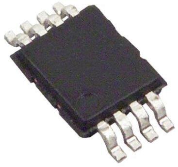
| 描述 | IC DIFF ADC DVR LOW DISTOR 8MSOP差分放大器 Low Distort ADC DVR |
| 产品分类 | |
| 品牌 | Analog Devices |
| 产品手册 | |
| 产品图片 |
|
| rohs | 符合RoHS无铅 / 符合限制有害物质指令(RoHS)规范要求 |
| 产品系列 | 放大器 IC,差分放大器,Analog Devices AD8138AARMZ- |
| 数据手册 | |
| 产品型号 | AD8138AARMZ |
| 产品种类 | 差分放大器 |
| 供应商器件封装 | 8-MSOP |
| 包装 | 管件 |
| 可用增益调整 | 1 V/V |
| 商标 | Analog Devices |
| 安装类型 | 表面贴装 |
| 安装风格 | SMD/SMT |
| 封装 | Tube |
| 封装/外壳 | 8-TSSOP,8-MSOP(0.118",3.00mm 宽) |
| 封装/箱体 | MSOP |
| 工作电源电压 | 3 V, 5 V, 9 V |
| 工厂包装数量 | 50 |
| 应用 | 数据采集 |
| 最大功率耗散 | 550 mW |
| 最大双重电源电压 | +/- 5.5 V |
| 最大工作温度 | + 85 C |
| 最大输入电阻 | 6 MOhms at 5 V |
| 最小工作温度 | - 40 C |
| 标准包装 | 50 |
| 类型 | ADC 驱动器 |
| 设计资源 | |
| 输入补偿电压 | 2.5 mV at 5 V |
| 通道数量 | 1 Channel |
| 配用 | /product-detail/zh/AD8138AARMZ-EBZ/AD8138AARMZ-EBZ-ND/4866699/product-detail/zh/AD8138ARM-EBZ/AD8138ARM-EBZ-ND/2700351/product-detail/zh/AD8138AR-EBZ/AD8138AR-EBZ-ND/2700350/product-detail/zh/AD8138AAR-EBZ/AD8138AAR-EBZ-ND/2700349 |


- 商务部:美国ITC正式对集成电路等产品启动337调查
- 曝三星4nm工艺存在良率问题 高通将骁龙8 Gen1或转产台积电
- 太阳诱电将投资9.5亿元在常州建新厂生产MLCC 预计2023年完工
- 英特尔发布欧洲新工厂建设计划 深化IDM 2.0 战略
- 台积电先进制程称霸业界 有大客户加持明年业绩稳了
- 达到5530亿美元!SIA预计今年全球半导体销售额将创下新高
- 英特尔拟将自动驾驶子公司Mobileye上市 估值或超500亿美元
- 三星加码芯片和SET,合并消费电子和移动部门,撤换高东真等 CEO
- 三星电子宣布重大人事变动 还合并消费电子和移动部门
- 海关总署:前11个月进口集成电路产品价值2.52万亿元 增长14.8%


PDF Datasheet 数据手册内容提取
Low Distortion, Differential ADC Driver Data Sheet AD8138 FEATURES PIN CONFIGURATION Easy to use, single-ended-to-differential conversion –IN 1 8 +IN Adjustable output common-mode voltage VOCM 2 7 NC Externally adjustable gain V+ 3 6 V– Lo−w9 h4a drBmco SnFiDc Rd iastt 5o rMtiHozn +OUT N4C=ANDO8C1O3N8NECT5 –OUT 01073-001 −85 dBc SFDR at 20 MHz Figure 1. −3 dB bandwidth of 320 MHz, G = +1 TYPICAL APPLICATION CIRCUIT Fast settling to 0.01% of 16 ns Slew rate 1150 V/µs 5V 5V Fast overdrive recovery of 4 ns 499Ω Low input voltage noise of 5 nV/√Hz 499Ω 1W midVe tsyuppipcalyl roafnfsgeet v+o3l Vta tgoe ± 5 V VIN 499VΩOCM +AD8138 AIN AVADDDCDVDD DOIUGTITPAULTS Low power 90 mW on 5 V – AIN AVSS VREF 0A.v1a dilBab glaei inn f 8la-tLneeasds StOo I4C0 a MndH zM SOP packages 499Ω 01073-002 Figure 2. APPLICATIONS ADC drivers Single-ended-to-differential converters IF and baseband gain blocks Differential buffers Line drivers GENERAL DESCRIPTION The AD8138 is a major advancement over op amps for The AD8138 eliminates the need for a transformer with high differential signal processing. The AD8138 can be used as a performance ADCs, preserving the low frequency and dc infor- single-ended-to-differential amplifier or as a differential-to- mation. The common-mode level of the differential output is differential amplifier. The AD8138 is as easy to use as an op adjustable by a voltage on the V pin, easily level-shifting the OCM amp and greatly simplifies differential signal amplification and input signals for driving single-supply ADCs. Fast overload driving. Manufactured on the proprietary ADI XFCB bipolar recovery preserves sampling accuracy. process, the AD8138 has a −3 dB bandwidth of 320 MHz and The AD8138 distortion performance makes it an ideal ADC delivers a differential signal with the lowest harmonic distortion driver for communication systems, with distortion performance available in a differential amplifier. The AD8138 has a unique good enough to drive state-of-the-art 10-bit to 16-bit converters internal feedback feature that provides balanced output gain at high frequencies. The high bandwidth and IP3 of the and phase matching, suppressing even order harmonics. The AD8138 also make it appropriate for use as a gain block in IF internal feedback circuit also minimizes any gain error that and baseband signal chains. The AD8138 offset and dynamic would be associated with the mismatches in the external gain performance makes it well suited for a wide variety of signal setting resistors. processing and data acquisition applications. The differential output of the AD8138 helps balance the input The AD8138 is available in both SOIC and MSOP packages for to differential ADCs, maximizing the performance of the ADC. operation over −40°C to +85°C temperatures. Rev. G Document Feedback Information furnished by Analog Devices is believed to be accurate and reliable. However, no responsibility is assumed by Analog Devices for its use, nor for any infringements of patents or other One Technology Way, P.O. Box 9106, Norwood, MA 02062-9106, U.S.A. rights of third parties that may result from its use. Specifications subject to change without notice. No license is granted by implication or otherwise under any patent or patent rights of Analog Devices. Tel: 781.329.4700 ©1999–2016 Analog Devices, Inc. All rights reserved. Trademarks and registered trademarks are the property of their respective owners. Technical Support www.analog.com
AD8138 Data Sheet TABLE OF CONTENTS Features .............................................................................................. 1 Definition of Terms .................................................................... 16 Applications ....................................................................................... 1 Theory of Operation ...................................................................... 17 Pin Configuration ............................................................................. 1 Analyzing an Application Circuit ............................................ 17 Typical Application Circuit ............................................................. 1 Setting the Closed-Loop Gain .................................................. 17 General Description ......................................................................... 1 Estimating the Output Noise Voltage ...................................... 17 Revision History ............................................................................... 2 The Impact of Mismatches in the Feedback Networks ......... 18 Specifications ..................................................................................... 3 Calculating the Input Impedance of an Application ............. 18 ±D to ±OUT Specifications ...................................................... 3 Input Common-Mode Voltage Range in Single-Supply IN Applications ................................................................................ 18 V to ±OUT Specifications ..................................................... 4 OCM Setting the Output Common-Mode Voltage .......................... 18 ±D to ±OUT Specifications ...................................................... 5 IN Driving a Capacitive Load ......................................................... 18 V to ±OUT Specifications ..................................................... 6 OCM Layout, Grounding, and Bypassing .............................................. 19 Absolute Maximum Ratings ............................................................ 7 Balanced Transformer Driver ....................................................... 20 Thermal Resistance ...................................................................... 7 High Performance ADC Driving ................................................. 21 ESD Caution .................................................................................. 7 3 V Operation ................................................................................. 22 Pin Configuration and Function Descriptions ............................. 8 Outline Dimensions ....................................................................... 23 Typical Performance Characteristics ............................................. 9 Ordering Guide .......................................................................... 23 Test Circuits ..................................................................................... 15 Operational Description ................................................................ 16 REVISION HISTORY Added New Paragraph after Table I ............................................. 10 3/16—Rev. F to Rev. G Updated Outline Dimensions ....................................................... 14 Changes to Setting the Closed-Loop Gain Section .................... 17 Changes to Figure 46 ...................................................................... 21 7/02—Rev. C to Rev. D Changes to Figure 47 ...................................................................... 22 Addition of TPC 35 and TPC 36 ..................................................... 8 1/06—Rev. E to Rev. F 6/01—Rev. B to Rev. C Changes to Features .......................................................................... 1 Edits to Specifications ...................................................................... 2 Added Thermal Resistance Section and Maximum Power Edits to Ordering Guide ................................................................... 4 Dissipation Section ........................................................................... 7 Changes to Balanced Transformer Driver Section ..................... 20 12/00—Rev. A to Rev. B Changes to Ordering Guide .......................................................... 23 9/99—Rev. 0 to Rev. A 3/03—Rev. D to Rev. E Changes to Specifications ................................................................ 2 3/99—Rev. 0: Initial Version Changes to Ordering Guide ............................................................ 4 Changes to TPC 16 ........................................................................... 6 Changes to Table I ............................................................................ 9 Rev. G | Page 2 of 24
Data Sheet AD8138 SPECIFICATIONS ±D TO ±OUT SPECIFICATIONS IN At 25°C, V = ±5 V, V = 0, G = +1, R = 500 Ω, unless otherwise noted. Refer to Figure 39 for test setup and label descriptions. All S OCM L, dm specifications refer to single-ended input and differential outputs, unless otherwise noted. Table 1. Parameter Conditions Min Typ Max Unit DYNAMIC PERFORMANCE −3 dB Small Signal Bandwidth V = 0.5 V p-p, C = 0 pF 290 320 MHz OUT F V = 0.5 V p-p, C = 1 pF 225 MHz OUT F Bandwidth for 0.1 dB Flatness V = 0.5 V p-p, C = 0 pF 30 MHz OUT F Large Signal Bandwidth V = 2 V p-p, C = 0 pF 265 MHz OUT F Slew Rate V = 2 V p-p, C = 0 pF 1150 V/µs OUT F Settling Time 0.01%, V = 2 V p-p, C = 1 pF 16 ns OUT F Overdrive Recovery Time V = 5 V to 0 V step, G = +2 4 ns IN NOISE/HARMONIC PERFORMANCE1 Second Harmonic V = 2 V p-p, 5 MHz, R = 800 Ω −94 dBc OUT L, dm V = 2 V p-p, 20 MHz, R = 800 Ω −87 dBc OUT L, dm V = 2 V p-p, 70 MHz, R = 800 Ω −62 dBc OUT L, dm Third Harmonic V = 2 V p-p, 5 MHz, R = 800 Ω −114 dBc OUT L, dm V = 2 V p-p, 20 MHz, R = 800 Ω −85 dBc OUT L, dm V = 2 V p-p, 70 MHz, R = 800 Ω −57 dBc OUT L, dm IMD 20 MHz −77 dBc IP3 20 MHz 37 dBm Voltage Noise (RTI) f = 100 kHz to 40 MHz 5 nV/√Hz Input Current Noise f = 100 kHz to 40 MHz 2 pA/√Hz INPUT CHARACTERISTICS Offset Voltage V = V /2; V = V = V = 0 V −2.5 ±1 +2.5 mV OS, dm OUT, dm DIN+ DIN− OCM T to T variation ±4 µV/°C MIN MAX Input Bias Current 3.5 7 µA T to T variation −0.01 µA/°C MIN MAX Input Resistance Differential 6 MΩ Common mode 3 MΩ Input Capacitance 1 pF Input Common-Mode Voltage −4.7 to +3.4 V CMRR ∆V /∆V ; ∆V = ±1 V −77 −70 dB OUT, dm IN, cm IN, cm OUTPUT CHARACTERISTICS Output Voltage Swing Maximum ∆V ; single-ended output 7.75 V p-p OUT Output Current 95 mA Output Balance Error ∆V /∆V ; ∆V = 1 V −66 dB OUT, cm OUT, dm OUT, dm 1 Harmonic distortion performance is equal or slightly worse with higher values of RL, dm. See Figure 17 and Figure 18 for more information. Rev. G | Page 3 of 24
AD8138 Data Sheet V TO ±OUT SPECIFICATIONS OCM At 25°C, V = ±5 V, V = 0, G = +1, R = 500 Ω, unless otherwise noted. Refer to Figure 39 for test setup and label descriptions. All S OCM L, dm specifications refer to single-ended input and differential outputs, unless otherwise noted. Table 2. Parameter Conditions Min Typ Max Unit DYNAMIC PERFORMANCE −3 dB Bandwidth 250 MHz Slew Rate 330 V/µs INPUT VOLTAGE NOISE (RTI) f = 0.1 MHz to 100 MHz 17 nV/√Hz DC PERFORMANCE Input Voltage Range ±3.8 V Input Resistance 200 kΩ Input Offset Voltage V = V ; V = V = V = 0 V –3.5 ±1 +3.5 mV OS, cm OUT, cm DIN+ DIN– OCM Input Bias Current 0.5 µA V CMRR ∆V /∆V ; ∆V = ±1 V −75 dB OCM OUT, dm OCM OCM Gain ∆V /∆V ; ∆V = ±1 V 0.9955 1 1.0045 V/V OUT, cm OCM OCM POWER SUPPLY Operating Range ±1.4 ±5.5 V Quiescent Current 18 20 23 mA T to T variation 40 µA/°C MIN MAX Power Supply Rejection Ratio ∆V /∆V; ∆V = ±1 V −90 −70 dB OUT, dm S S OPERATING TEMPERATURE RANGE −40 +85 °C Rev. G | Page 4 of 24
Data Sheet AD8138 ±D TO ±OUT SPECIFICATIONS IN At 25°C, V = 5 V, V = 2.5 V, G = +1, R = 500 Ω, unless otherwise noted. Refer to Figure 39 for test setup and label descriptions. All S OCM L, dm specifications refer to single-ended input and differential output, unless otherwise noted. Table 3. Parameter Conditions Min Typ Max Unit DYNAMIC PERFORMANCE −3 dB Small Signal Bandwidth V = 0.5 V p-p, C = 0 pF 280 310 MHz OUT F V = 0.5 V p-p, C = 1 pF 225 MHz OUT F Bandwidth for 0.1 dB Flatness V = 0.5 V p-p, C = 0 pF 29 MHz OUT F Large Signal Bandwidth V = 2 V p-p, C = 0 pF 265 MHz OUT F Slew Rate V = 2 V p-p, C = 0 pF 950 V/µs OUT F Settling Time 0.01%, V = 2 V p-p, C = 1 pF 16 ns OUT F Overdrive Recovery Time V = 2.5 V to 0 V step, G = +2 4 ns IN NOISE/HARMONIC PERFORMANCE1 Second Harmonic V = 2 V p-p, 5 MHz, R = 800 Ω −90 dBc OUT L, dm V = 2 V p-p, 20 MHz, R = 800 Ω −79 dBc OUT L, dm V = 2 V p-p, 70 MHz, R = 800 Ω −60 dBc OUT L, dm Third Harmonic V = 2 V p-p, 5 MHz, R = 800 Ω −100 dBc OUT L, dm V = 2 V p-p, 20 MHz, R = 800 Ω −82 dBc OUT L, dm V = 2 V p-p, 70 MHz, R = 800 Ω −53 dBc OUT L, dm IMD 20 MHz −74 dBc IP3 20 MHz 35 dBm Voltage Noise (RTI) f = 100 kHz to 40 MHz 5 nV/√Hz Input Current Noise f = 100 kHz to 40 MHz 2 pA/√Hz INPUT CHARACTERISTICS Offset Voltage V = V /2; V = V = V = 0 V −2.5 ±1 +2.5 mV OS, dm OUT, dm DIN+ DIN– OCM T to T variation ±4 µV/°C MIN MAX Input Bias Current 3.5 7 µA T to T variation −0.01 µA/°C MIN MAX Input Resistance Differential 6 MΩ Common mode 3 MΩ Input Capacitance 1 pF Input Common-Mode Voltage −0.3 to +3.2 V CMRR ∆V /∆V ; ∆V = 1 V −77 −70 dB OUT, dm IN, cm IN, cm OUTPUT CHARACTERISTICS Output Voltage Swing Maximum ∆V ; single-ended output 2.9 V p-p OUT Output Current 95 mA Output Balance Error ∆V /∆V ; ∆V = 1 V −65 dB OUT, cm OUT, dm OUT, dm 1 Harmonic distortion performance is equal or slightly worse with higher values of RL, dm. See Figure 17 and Figure 18 for more information. Rev. G | Page 5 of 24
AD8138 Data Sheet V TO ±OUT SPECIFICATIONS OCM At 25°C, V = 5 V, V = 2.5 V, G = +1, R = 500 Ω, unless otherwise noted. Refer to Figure 39 for test setup and label descriptions. All S OCM L, dm specifications refer to single-ended input and differential output, unless otherwise noted. Table 4. Parameter Conditions Min Typ Max Unit DYNAMIC PERFORMANCE −3 dB Bandwidth 220 MHz Slew Rate 250 V/µs INPUT VOLTAGE NOISE (RTI) f = 0.1 MHz to 100 MHz 17 nV/√Hz DC PERFORMANCE Input Voltage Range 1.0 to 3.8 V Input Resistance 100 kΩ Input Offset Voltage V = V ; V = V = V = 0 V −5 ±1 +5 mV OS, cm OUT, cm DIN+ DIN– OCM Input Bias Current 0.5 µA V CMRR ∆V /∆V ; ∆V = 2.5 V ±1 V −70 dB OCM OUT, dm OCM OCM Gain ∆V /∆V ; ∆V = 2.5 V ±1 V 0.9968 1 1.0032 V/V OUT, cm OCM OCM POWER SUPPLY Operating Range 2.7 11 V Quiescent Current 15 20 21 mA T to T variation 40 µA/°C MIN MAX Power Supply Rejection Ratio ∆V /∆V; ∆V = ± 1 V −90 −70 dB OUT, dm S S OPERATING TEMPERATURE RANGE −40 +85 °C Rev. G | Page 6 of 24
Data Sheet AD8138 ABSOLUTE MAXIMUM RATINGS The power dissipated in the package (P ) is the sum of the Table 5. D quiescent power dissipation and the power dissipated in the Parameter Ratings package due to the load drive for all outputs. The quiescent Supply Voltage ±5.5 V power is the voltage between the supply pins (V) times the V ±V S OCM S quiescent current (I). The load current consists of the differential Internal Power Dissipation 550 mW S and common-mode currents flowing to the load, as well as Operating Temperature Range −40°C to +85°C currents flowing through the external feedback networks and Storage Temperature Range −65°C to +150°C internal common-mode feedback loop. The internal resistor tap Lead Temperature (Soldering 10 sec) 300°C used in the common-mode feedback loop places a negligible Junction Temperature 150°C differential load on the output. RMS voltages and currents Stresses at or above those listed under Absolute Maximum should be considered when dealing with ac signals. Ratings may cause permanent damage to the product. This is a stress rating only; functional operation of the product at these Airflow reduces θJA. In addition, more metal directly in contact or any other conditions above those indicated in the operational with the package leads from metal traces through holes, ground, section of this specification is not implied. Operation beyond and power planes reduces the θJA. the maximum operating conditions for extended periods may Figure 3 shows the maximum safe power dissipation in the affect product reliability. package vs. the ambient temperature for the 8-lead SOIC THERMAL RESISTANCE (121°C/W) and 8-lead MSOP (θ = 145°C/W) packages on a JA JEDEC standard 4-layer board. θ values are approximations. θ is specified for the worst-case conditions, that is, θ is JA JA JA specified for the device soldered in a circuit board in still air. 1.75 Table 6. W) 1.50 N ( Package Type θ Unit O JA TI 1.25 8-Lead SOIC/4-Layer 121 °C/W PA SI 8-Lead MSOP/4-Layer 145 °C/W DIS 1.00 SOIC ER W 0.75 Maximum Power Dissipation PO MSOP M The maximum safe power dissipation in the AD8138 packages MU 0.50 XI is limited by the associated rise in junction temperature (T) on A J M 0.25 the die. At approximately 150°C, which is the glass transition teexmcepeedriantugr teh, itsh ete pmlapsetirca ctuhraen gliems iitts c parno pcheratniegse. Ethveen s ttreemsspeosr tahrialty the 0–40–30–20–10 0AM10BIE2N0T3T0EM40PE5R0AT6U0RE70(°C80) 90 100110120 01073-049 package exerts on the die, permanently shifting the parametric Figure 3. Maximum Power Dissipation vs. Temperature performance of the AD8138. Exceeding a junction temperature ESD CAUTION of 150°C for an extended period can result in changes in the silicon devices, potentially causing failure. Rev. G | Page 7 of 24
AD8138 Data Sheet PIN CONFIGURATION AND FUNCTION DESCRIPTIONS –IN 1 8 +IN VOCM 2 7 NC V+ 3 6 V– +OUT N4C=ANDO8C1O3N8NECT5 –OUT 01073-004 Figure 4. Pin Configuration Table 7. Pin Function Descriptions Pin No. Mnemonic Description 1 −IN Negative Input Summing Node. 2 V Voltage applied to this pin sets the common-mode output voltage with a ratio of 1:1. For example, OCM 1 V dc on V sets the dc bias level on +OUT and −OUT to 1 V. OCM 3 V+ Positive Supply Voltage. 4 +OUT Positive Output. Note that the voltage at −D is inverted at +OUT (see Figure 42). IN 5 −OUT Negative Output. Note that the voltage at +D is inverted at −OUT (see Figure 42). IN 6 V− Negative Supply Voltage. 7 NC No Connect. 8 +IN Positive Input Summing Node. Rev. G | Page 8 of 24
Data Sheet AD8138 TYPICAL PERFORMANCE CHARACTERISTICS Unless otherwise noted, Gain = 1, R = R = R = 499 V, T = 25°C; refer to Figure 39 for test setup. G F L, dm A 6 6 VIN=0.2Vp-p VIN=2Vp-p CF=0pF CF=0pF 3 3 VS=+5V VS=+5V B) 0 B) 0 d d AIN ( VS=±5V AIN ( VS=±5V G G –3 –3 –6 –6 –91 10FREQUENCY(MHz1)00 1000 01073-005 –9 1 10FREQUENCY(MHz1)00 1000 01073-008 Figure 5. Small Signal Frequency Response Figure 8. Large Signal Frequency Response 6 6 VS=±5V VIN=2Vp-p VIN=0.2Vp-p VS=±5V 3 3 CF=0pF CF=0pF B) 0 B) 0 GAIN (d CF=1pF GAIN (d CF=1pF –3 –3 –6 –6 –91 10FREQUENCY(MHz1)00 1000 01073-006 –91 10FREQUENCY(MHz1)00 1000 01073-009 Figure 6. Small Signal Frequency Response Figure 9. Large Signal Frequency Response 0.5 30 VVSIN==±05.V2Vp-p VCVSOFU==T±0,d5pmVF=0.2Vp-p 0.3 RG=499Ω CF=0pF 20 G=10,RF=4.99kΩ G=5,RF=2.49kΩ B) 0.1 B) d d N ( N ( 10 GAI GAI G=2,RF=1kΩ –0.1 CF=1pF G=1,RF=499Ω 0 –0.3 –0.51 FREQUE1N0CY(MHz) 100 01073-007 –101 10FREQUENCY(MHz1)00 1000 01073-010 Figure 7. 0.1 dB Flatness vs. Frequency Figure 10. Small Signal Frequency Response for Various Gains Rev. G | Page 9 of 24
AD8138 Data Sheet –50 –60 VROLU=T8,d0m0Ω=2Vp-p VRSL==±850V0Ω –60 HD3(F=20MHz) –70 HD2(F=20MHz) –70 Bc) HD2(VS=+5V) Bc) –80 d d ON ( –80 HD2(VS=±5V) ON ( TI TI –90 R R O –90 O T T HD2(F=5MHz) S S DI DI–100 –100 HD3(VS=+5V) HD3(F=5MHz) –110 –110 HD3(VS=±5V) –1200 10 FUN2D0AMENT3A0LFREQ40UENCY5(M0Hz) 60 70 01073-011 –1200 1DIFFEREN2TIAL OUTP3UTVOLTA4GE(Vp-p5) 6 01073-014 Figure 11. Harmonic Distortion vs. Frequency Figure 14. Harmonic Distortion vs. Differential Output Voltage –40 –60 VOUT,dm=4Vp-p VS=5V RL=800Ω RL=800Ω –50 –70 HD3(VS=+5V) HD2(F=20MHz) –60 Bc) Bc) –80 d d HD3(F=20MHz) N ( –70 N ( ORTIO –80 HD2(VS=+5V) ORTIO –90 HD2(F=5MHz) T T DIS HD2(VS=±5V) DIS–100 –90 HD3(F=5MHz) –110 –100 HD3(VS=±5V) –1100 10 FUN2D0AMENT3A0LFREQ40UENCY5(M0Hz) 60 70 01073-012 –1200 DIFFE1RENTIAL OUTP2UTVOLTAGE(3Vp-p) 4 01073-015 Figure 12. Harmonic Distortion vs. Frequency Figure 15. Harmonic Distortion vs. Differential Output Voltage –30 –60 VOUT,dm=2Vp-p VS=3V RL=800Ω RL=800Ω –40 FO=20MHz –70 HD3(F=20MHz) –50 Bc) HD2(VS=+5V) Bc) HD2(F=20MHz) N (d –60 N (d –80 O O DISTORTI –70 HD3(VS=+5V) DISTORTI –90 HD2(F=5MHz) –80 HD3(VS=±5V) –100 HD3(F=5MHz) –90 HD2(VS=±5V) –100–4 –3 –2 VO–C1MDC O0UTPUT1(V) 2 3 4 01073-013 –1100.25 0.5D0IFFERE0N.7T5IAL OUT1.P0U0TVOL1T.A25GE(Vp1-p.5)0 1.75 01073-016 Figure 13. Harmonic Distortion vs. VOCM Figure 16. Harmonic Distortion vs. Differential Output Voltage Rev. G | Page 10 of 24
Data Sheet AD8138 –60 45 VS=5V RL=800Ω VOUT,dm=2Vp-p –70 40 HD2(F=20MHz) c) m) RTION (dB –80 HD3(F=20MHz) CEPT (dB 35 VS=±5V DISTO –90 HD2(F=5MHz) INTER VS=+5V 30 –100 HD3(F=5MHz) –110200 600 1R0L0O0AD(Ω) 1400 1800 01073-017 250 20 FREQUEN40CY(MHz) 60 80 01073-020 Figure 17. Harmonic Distortion vs. RLOAD Figure 20. Third-Order Intercept vs. Frequency –60 VS=±5V VS=±5V VOUT,dm=2Vp-p –70 HD2(F=20MHz) VOUT,dm Bc) –80 HD3(F=20MHz) VOUT– d N ( O RTI –90 VOUT+ O T HD2(F=5MHz) S DI–100 V+DIN HD3(F=5MHz) –110 –120 1V 5ns 01073-021 200 600 1R00LO0AD(Ω) 1400 1800 01073-018 Figure 18. Harmonic Distortion vs. RLOAD Figure 21. Large Signal Transient Response 10 FVCS==5±05MVHz CF=0pF VVOSU=T±,d5mV=0.2Vp-p –10 –30 CF=1pF m) B d (UT –50 O P –70 –90 –11049.5 49.7 FR49E.Q9UENCY(5M0H.1z) 50.3 50.5 01073-019 40mV 5ns 01073-022 Figure 19. Intermodulation Distortion Figure 22. Small Signal Transient Response Rev. G | Page 11 of 24
AD8138 Data Sheet VS=±5V VOUT,dm=2Vp-p CF=0pF VOUT,dm VS=+5V VS=±5V F=20MHz V+DIN=8Vp-p G=3(RF=1500) V+DIN 400mV 5ns 01073-023 4V 30ns 01073-026 Figure 23. Large Signal Transient Response Figure 26. Output Overdrive CF=0pF VOUT,dm=2Vp-p VS=±5V VS=±5V CF=0pF CL=10pF CL=5pF CF=1pF CL=20pF 400mV 5ns 01073-024 400mV 2.5ns 01073-028 Figure 24. Large Signal Transient Response Figure 27. Large Signal Transient Response for Various Cap Loads (See Figure 40) –20 VS=±5V 200µV VS=±5V ∆VOUT,dm/∆VIN,cm CF=1pF –30 VOUT,dm –40 B) d R ( –50 R M C –60 V+DIN –70 1V 4ns 01073-025 –801 10FREQUENCY(MHz1)00 1k 01073-029 Figure 25. Settling Time Figure 28. CMRR vs. Frequency Rev. G | Page 12 of 24
Data Sheet AD8138 –20 5.0 VIN=2Vp-p V) m –30 T ( E 2.5 R (dB) OFFS VS=±5V O –40 T RR PU VS=+5V ANCE E –50 VS=±5V AL OUT 0 AL NTI VS=+3V B E ER–2.5 –60 VS=+5V FF DI –701 10FREQUENCY(MHz1)00 1k 01073-031 –5.0–40 –20 0 TEM2P0ERATUR4E0(°C) 60 80 100 01073-034 Figure 29. Output Balance Error vs. Frequency (See Figure 41) Figure 32. Output Referred Differential Offset Voltage vs. Temperature –10 5 ΔVOUT,dm/ΔVS –20 –30 4 –PSRR RR (dB) ––4500 (VS=±5V) RRENT (µA) 3 VS=±5V,+5V S U P C –60 +PSRR AS VS=+3V (VS=+5V,0VAND±5V) BI –70 2 –80 –901 10FREQUENCY(MHz1)00 1k 01073-032 1–40 –20 0 TEM2P0ERATUR4E0(°C) 60 80 100 01073-035 Figure 30. PSRR vs. Frequency Figure 33. Input Bias Current vs. Temperature 100 30 SINGLE-ENDED OUTPUT 25 A) Ω) 10 T (m VS=±5V E ( EN 20 C R AN VS=+5V UR MPED PLY C 15 VS=+5V I 1 P SU VS=+3V VS=±5V 10 0.11 FREQUE1N0CY(MHz) 100 01073-033 5–40 –20 0 TEM2P0ERATUR4E0(°C) 60 80 100 01073-036 Figure 31. Output Impedance vs. Frequency Figure 34. Supply Current vs. Temperature Rev. G | Page 13 of 24
AD8138 Data Sheet 6 100 VS=+5V 3 VS=±5V Hz) A/ p E ( B) 0 OIS d N AIN ( ENT 10 G –3 RR U C T 1.1pA/ Hz U P –6 N I –91 10FREQUENCY(MHz1)00 1k 01073-037 110 100 FR1kEQUENCY1(H0kz) 100k 1M 01073-039 Figure 35. VOCM Frequency Response Figure 37. Current Noise (RTI) 1000 VS=±5V VOCM=–1VTO+1V Hz) V/ VOUT,cm E (n 100 S OI N E G A T L O V 10 5.7nV/ Hz T U P N I 400mV 5ns 01073-038 110 100 FR1kEQUENCY1(H0kz) 100k 1M 01073-040 Figure 36. VOCM Transient Response Figure 38. Voltage Noise (RTI) Rev. G | Page 14 of 24
Data Sheet AD8138 TEST CIRCUITS RF=499Ω 499Ω RG=499Ω 499Ω 249Ω 49.9ΩRG=499Ω AD8138 RL,dm=499Ω 49.9Ω499Ω AD8138 249Ω 24.9Ω RF=499Ω 01073-003 24.9Ω 499Ω 01073-030 Figure 39. Basic Test Circuit Figure 41. Test Circuit for Output Balance 499Ω 499Ω 24.9Ω 49.9Ω499Ω AD8138 24.9Ω CL 453Ω 24.9Ω 499Ω 01073-027 Figure 40. Test Circuit for Cap Load Drive Rev. G | Page 15 of 24
AD8138 Data Sheet OPERATIONAL DESCRIPTION DEFINITION OF TERMS Common-mode voltage refers to the average of two node CF voltages. The output common-mode voltage is defined as V = (V + V )/2 RF OUT, cm +OUT −OUT RG +IN –OUT Balance is a measure of how well differential signals are +DIN matched in amplitude and exactly 180° apart in phase. Balance VOCM AD8138 RL,dm VOUT,dm is most easily determined by placing a well-matched resistor –DIN RG –IN +OUT divider between the differential voltage nodes and comparing RF the magnitude of the signal at the midpoint of the divider with CF 01073-041 the magnitude of the differential signal (see Figure 41). By this definition, output balance is the magnitude of the output Figure 42. Circuit Definitions common-mode voltage divided by the magnitude of the output Differential voltage refers to the difference between two node differential mode voltage: voltages. For example, the output differential voltage (or V equivalently output differential-mode voltage) is defined as OutputBalanceError= OUT,cm V V = (V − V ) OUT,dm OUT, dm +OUT −OUT where V and V refer to the voltages at the +OUT and +OUT −OUT −OUT terminals with respect to a common reference. Rev. G | Page 16 of 24
Data Sheet AD8138 THEORY OF OPERATION The AD8138 differs from conventional op amps in that it has ANALYZING AN APPLICATION CIRCUIT two outputs whose voltages move in opposite directions. Like The AD8138 uses high open-loop gain and negative feedback to an op amp, it relies on high open-loop gain and negative force its differential and common-mode output voltages in such feedback to force these outputs to the desired voltages. The a way as to minimize the differential and common-mode error AD8138 behaves much like a standard voltage feedback op voltages. The differential error voltage is defined as the voltage amp and makes it easy to perform single-ended-to-differential between the differential inputs labeled +IN and −IN in Figure 42. conversion, common-mode level-shifting, and amplification of For most purposes, this voltage can be assumed to be zero. differential signals. Also like an op amp, the AD8138 has high Similarly, the difference between the actual output common- input impedance and low output impedance. mode voltage and the voltage applied to V can also be OCM assumed to be zero. Starting from these two assumptions, any Previous differential drivers, both discrete and integrated application circuit can be analyzed. designs, have been based on using two independent amplifiers and two independent feedback loops, one to control each of the SETTING THE CLOSED-LOOP GAIN outputs. When these circuits are driven from a single-ended Neglecting the capacitors C, the differential-mode gain of the source, the resulting outputs are typically not well balanced. F circuit in Figure 42 can be determined to be described by Achieving a balanced output has typically required exceptional matching of the amplifiers and feedback networks. V R S OUT,dm = F V R S DC common-mode level-shifting has also been difficult with IN,dm G previous differential drivers. Level-shifting has required the use This assumes the input resistors, R S, and feedback resistors, RS, of a third amplifier and feedback loop to control the output G F on each side are equal. common-mode level. Sometimes the third amplifier has also been used to attempt to correct an inherently unbalanced ESTIMATING THE OUTPUT NOISE VOLTAGE circuit. Excellent performance over a wide frequency range Similar to the case of a conventional op amp, the differential has proven difficult with this approach. output errors (noise and offset voltages) can be estimated by The AD8138 uses two feedback loops to separately control the multiplying the input referred terms, at +IN and −IN, by the differential and common-mode output voltages. The differential circuit noise gain. The noise gain is defined as feedback, set with external resistors, controls only the differential R output voltage. The common-mode feedback controls only the G =1+ F common-mode output voltage. This architecture makes it easy N RG to arbitrarily set the output common-mode level. It is forced, by To compute the total output referred noise for the circuit of internal common-mode feedback, to be equal to the voltage Figure 42, consideration must also be given to the contribution applied to the V input, without affecting the differential OCM of the Resistors R and R . Refer to Table 8 for the estimated output voltage. F G output noise voltage densities at various closed-loop gains. The AD8138 architecture results in outputs that are very highly balanced over a wide frequency range without requiring tightly matched external components. The common-mode feedback loop forces the signal component of the output common-mode voltage to be zeroed. The result is nearly perfectly balanced differential outputs of identical amplitude and exactly 180°apart in phase. Table 8. Gain R (Ω) R (Ω) Bandwidth −3 dB Output Noise AD8138 Only Output Noise AD8138 + R , R G F G F 1 499 499 320 MHz 10 nV/√Hz 11.6 nV/√Hz 2 499 1.0 k 180 MHz 15 nV/√Hz 18.2 nV/√Hz 5 499 2.49 k 70 MHz 30 nV/√Hz 37.9 nV/√Hz 10 499 4.99 k 30 MHz 55 nV/√Hz 70.8 nV/√Hz Rev. G | Page 17 of 24
AD8138 Data Sheet When using the AD8138 in gain configurations where R/R of CALCULATING THE INPUT IMPEDANCE OF AN F G one feedback network is unequal to R/R of the other network, APPLICATION F G there is a differential output noise due to input-referred voltage The effective input impedance of a circuit such as the one in in the V circuitry. The output noise is defined in terms of OCM Figure 42, at +DIN and –DIN, depends on whether the amplifier is the following feedback terms (refer to Figure 42): being driven by a single-ended or differential signal source. For R balanced differential input signals, the input impedance (R ) β = G IN, dm 1 RF +RG between the inputs (+DIN and −DIN) is simply R =2 × R IN, dm G for −OUT to +IN loop, and R In the case of a single-ended input signal (for example if −DIN is β = G 2 R +R grounded and the input signal is applied to +DIN), the input F G impedance becomes for +OUT to −IN loop. With these defined, V =2V β1−β2 RIN,dm= RGR nOUT,dm nIN,VOCMβ1+β2 1−2×(R F+R ) G F where VnOUT, dm is the output differential noise, and VnIN,VCOM is The input impedance of the circuit is effectively higher than it the input-referred voltage noise in VOCM. would be for a conventional op amp connected as an inverter because a fraction of the differential output voltage appears at THE IMPACT OF MISMATCHES IN THE FEEDBACK the inputs as a common-mode signal, partially bootstrapping NETWORKS the voltage across the input resistor R . G As previously mentioned, even if the external feedback INPUT COMMON-MODE VOLTAGE RANGE IN networks (R/R ) are mismatched, the internal common-mode F G SINGLE-SUPPLY APPLICATIONS feedback loop still forces the outputs to remain balanced. The amplitudes of the signals at each output remains equal and 180° The AD8138 is optimized for level-shifting, ground-referenced out of phase. The input-to-output differential-mode gain varies input signals. For a single-ended input, this would imply, for proportionately to the feedback mismatch, but the output example, that the voltage at −D in Figure 42 would be 0 V IN balance is unaffected. when the negative power supply voltage of the amplifier (at V−) is also set to 0 V. Ratio matching errors in the external resistors result in a degradation of the ability of the circuit to reject input common- SETTING THE OUTPUT COMMON-MODE VOLTAGE mode signals, much the same as for a four-resistor difference The V pin of the AD8138 is internally biased at a voltage OCM amplifier made from a conventional op amp. approximately equal to the midsupply point (average value of In addition, if the dc levels of the input and output common- the voltages on V+ and V−). Relying on this internal bias results mode voltages are different, matching errors result in a small in an output common-mode voltage that is within about differential-mode output offset voltage. For the G = 1 case, with 100 mV of the expected value. a ground referenced input signal and the output common-mode In cases where more accurate control of the output common- level set for 2.5 V, an output offset of as much as 25 mV (1% of mode level is required, it is recommended that an external the difference in common-mode levels) can result if 1% tolerance source, or resistor divider (made up of 10 kΩ resistors), be used. resistors are used. Resistors of 1% tolerance result in a worst- The output common-mode offset listed in the Specifications case input CMRR of about 40 dB, worst-case differential mode section assumes the V input is driven by a low impedance OCM output offset of 25 mV due to 2.5 V level-shift, and no significant voltage source. degradation in output balance error. DRIVING A CAPACITIVE LOAD A purely capacitive load can react with the pin and bondwire inductance of the AD8138, resulting in high frequency ringing in the pulse response. One way to minimize this effect is to place a small capacitor across each of the feedback resistors. The added capacitance should be small to avoid destabilizing the amplifier. An alternative technique is to place a small resistor in series with the outputs of the amplifier, as shown in Figure 40. Rev. G | Page 18 of 24
Data Sheet AD8138 LAYOUT, GROUNDING, AND BYPASSING As a high speed device, the AD8138 is sensitive to the PCB The power supply pins should be bypassed as close as possible environment in which it has to operate. Realizing its superior to the device to the nearby ground plane. Good high frequency specifications requires attention to various details of good high ceramic chip capacitors should be used. This bypassing should speed PCB design. be done with a capacitance value of 0.01 µF to 0.1 µF for each supply. Further away, low frequency bypassing should be provided The first requirement is for a good solid ground plane that with 10 µF tantalum capacitors from each supply to ground. covers as much of the board area around the AD8138 as possible. The only exception to this is that the two input pins The signal routing should be short and direct to avoid parasitic (Pin 1 and Pin 8) should be kept a few millimeters from the effects. Wherever there are complementary signals, a symmetrical ground plane, and ground should be removed from inner layers layout should be provided to the extent possible to maximize and the opposite side of the board under the input pins. This the balance performance. When running differential signals minimizes the stray capacitance on these nodes and helps over a long distance, the traces on the PCB should be close preserve the gain flatness vs. frequency. together or any differential wiring should be twisted together to minimize the area of the loop that is formed. This reduces the radiated energy and makes the circuit less susceptible to interference. Rev. G | Page 19 of 24
AD8138 Data Sheet BALANCED TRANSFORMER DRIVER Transformers are among the oldest devices used to perform a The well-balanced outputs of the AD8138 provide a drive signal single-ended-to-differential conversion (and vice versa). Trans- to each of the primary inputs of the transformer that are of formers can also perform the additional functions of galvanic equal amplitude and 180° out of phase. Therefore, depending isolation, step-up or step-down of voltages, and impedance on how the polarity of the secondary is connected, the signals transformation. For these reasons, transformers always find that conduct across the interwinding capacitance either both uses in certain applications. assist the secondary signal of the transformer equally, or both buck the secondary signals. In either case, the parasitic effect is However, when driving the transformer in a single-ended symmetrical and provides a well-balanced transformer output manner, there is an imbalance at the output due to the parasitics (see Figure 45). inherent in the transformer. The primary (or driven) side of the transformer has one side at dc potential (usually ground), while ONSTIGHNISALS IIDSECVOIAUPCLSETDRAY the other side is driven. This can cause problems in systems that CSTRAY require good balance of the differential output signals of the transformer. VUNBAL 500.000Ω5% 52.3Ω PRIMARY 500Ω SECONDARYVDIFF If the interwinding capacitance (C ) is assumed to be 0.005% STRAY uniformly distributed, a signal from the driving source couples CSTRAY tsoid teh oe fs tehceo npdriamrya royu. tOpunt ttheer motihnearl hthaantd i,s ncolo ssiegsnt atlo i tsh ceo durpilveedn t o NOSIOGNNATLH IISSSCIODUEPLED 01073-042 Figure 43. Transformer Single-Ended-to-Differential Converter Is Inherently the opposite terminal of the secondary because its nearest Imbalanced primary terminal is not driven (see Figure 43). The exact amount of this imbalance depends on the particular parasitics 499Ω of the trans-former, but is mostly a problem at higher CSTRAY frequencies. 49.9Ω The balance of a differential circuit can be measured by 499Ω +IN OUT– VUNBAL 500.000Ω5% connecting an equal-valued resistive voltage divider across the 499Ω AD8138 500Ω VDIFF OUT+ 0.005% differential outputs and then measuring the center point of the –IN 49.9Ω cairrec suuitp wpoitshe dre tsop becet o tfo e gqruoauln adm. pSilnitcued teh, eb utwt 1o8 d0i°f foeprepnotsiiatle opuhtapsuet,s 499Ω CSTRAY 01073-043 there should be no signal present for perfectly balanced outputs. Figure 44. AD8138 Forms a Balanced Transformer Driver The circuit in Figure 43 shows a Mini-Circuits® T1-6T 0 transformer connected with its primary driven single-endedly and the secondary connected with a precision voltage divider B)–20 d across its terminals. The voltage divider is made up of two R ( O a5l0s0o Ωeq, u0a.0l 0to5 %th pe raecc icsoiomnm reosnis-tmorosd. eT vhoel vtaogltea, gise aV mUNeBaAsL,u wreh oicf hh oisw E ERR–40 VWUITNBHASLI,NFGOLRET-ERNADNESDFODRRMIVEER C closely the outputs are balanced. AN L BA–60 Figure 45 compares the transformer being driven single- T U P endedly by a signal generator and being driven differentially T U O–80 using an AD8138. The top signal trace of Figure 45 shows the balance of the single-ended configuration, while the bottom VUNBAL,DIFFERENTIALDRIVE sbhaolawnsc eth ies 3d5if fdeBre bnettiatellry w dhrievne nu sbinalga nthcee AreDsp8o1n3s8e.. The 100 MHz –1000.3 1 FREQUENC1Y0(MHz) 100 500 01073-044 Figure 45. Output Balance Error for Circuits of Figure 43 and Figure 44 Rev. G | Page 20 of 24
Data Sheet AD8138 HIGH PERFORMANCE ADC DRIVING The circuit in Figure 46 shows a simplified front-end The signal generator has a ground-referenced, bipolar output, connection for an AD8138 driving an AD9224, a 12-bit, that is, it drives symmetrically above and below ground. 40 MSPS ADC. The ADC works best when driven differentially, Connecting V to the CML pin of the AD9224 sets the output OCM which minimizes its distortion. The AD8138 eliminates the common-mode of the AD8138 at 2.5 V, which is the midsupply need for a transformer to drive the ADC and performs single- level for the AD9224. This voltage is bypassed by a 0.1 µF ended-to-differential conversion, common-mode level-shifting, capacitor. and buffering of the driving signal. The full-scale analog input range of the AD9224 is set to The positive and negative outputs of the AD8138 are connected 4 V p-p, by shorting the SENSE terminal to AVSS. This has to the respective differential inputs of the AD9224 via a pair of been determined to be the scaling to provide minimum 49.9 Ω resistors to minimize the effects of the switched-capacitor harmonic distortion. front end of the AD9224. For best distortion performance, it For the AD8138 to swing at 4 V p-p, each output swings 2 V p-p runs from supplies of ±5 V. while providing signals that are 180° out of phase. With a The AD8138 is configured with unity gain for a single-ended, common-mode voltage at the output of 2.5 V, each AD8138 input-to-differential output. The additional 23 Ω, 523 Ω total, at output swings between 1.5 V and 3.5 V. the input to −IN is to balance the parallel impedance of the A ground-referenced 4 V p-p, 5 MHz signal at D + was used to 50 Ω source and its 50 Ω termination that drives the IN test the circuit in Figure 46. When the combined-device circuit noninverting input. was run with a sampling rate of 20 MSPS, the spurious-free dynamic range (SFDR) was measured at −85 dBc. +5V +5V 499Ω 0.1µF 0.1µF 15 26 28 499Ω 3 49.9Ω 8 + 5 24 VINB AVDD DRVDD SOUR5C0ΩE 49.9Ω 2 ADVO8C1M38 AD9224 DOIUGTITPAULTS 523Ω 49.9Ω 1 4 23 VINA AVSS SENSE CML DRVSS 6 0.1µF 16 25 17 22 27 499Ω –5V 01073-045 Figure 46. AD8138 Driving an AD9224, a 12-Bit, 40 MSPS ADC Rev. G | Page 21 of 24
AD8138 Data Sheet 3 V OPERATION The circuit in Figure 47 shows a simplified front-end The circuit was tested with a −0.5 dBFS signal at various connection for an AD8138 driving an AD9203, a 10-bit, frequencies. Figure 48 shows a plot of the total harmonic 40 MSPS ADC that is specified to work on a single 3 V supply. distortion (THD) vs. frequency at signal amplitudes of 1 V and The ADC works best when driven differentially to make the 2 V differential drive levels. best use of the signal swing available within the 3 V supply. –40 The appropriate outputs of the AD8138 are connected to the appropriate differential inputs of the AD9203 via a low-pass filter. –45 The AD8138 is configured for unity gain for a single-ended –50 input to differential output. The additional 23 Ω at the input to –55 −IN is to balance the impedance of the 50 Ω source and its 50 Ω Bc) AD8138–2V termination that drives the noninverting input. D (d–60 H T –65 The signal generator has ground-referenced, bipolar output, AD8138–1V that is, it can drive symmetrically above and below ground. –70 Even though the AD8138 has ground as its negative supply, it –75 can still function as a level-shifter with such an input signal. –80 Tvohleta oguet dpiuvti dcoerm tmhaot nb imasoeds eV is ra.i sIend t huips twoa my, itdhseu AppDly8 1b3y8 t he 0 5 FR1E0QUENCY(M15Hz) 20 25 01073-047 OCM Figure 48. AD9203 THD at −0.5 dBFS AD8138 provides dc coupling and level-shifting of a bipolar signal, without inverting the input signal. Figure 49 shows the signal-to-noise-and-distortion (SINAD) under the same conditions as above. For the smaller signal The low-pass filter between the AD8138 and the AD9203 swing, the AD8138 performance is quite good, but its provides filtering that helps to improve the signal-to-noise ratio performance degrades when trying to swing too close to the (SNR). Lower noise can be realized by lowering the pole supply rails. frequency, but the bandwidth of the circuit is lowered. 65 3V 3V 63 499Ω 0.1µF 0.1µF 0.1µF 61 10kΩ 49.9Ω 459293ΩΩ 82 +A3D81538 44992..099pΩΩF 25AAIINNANPV2D8DAD9D2R0V23DD DOIUGTITPAULTS AD (dBc) 555975 AD8138–1V 0.1µF 1 6 4 20pF 26 AV2S7S DRV1SS SIN 53 AD8138–2V 499Ω 51 10kΩ 01073-046 4497 Figure 47. AD8138 Driving an AD9203, a 10-Bit, 40 MSPS Analog-to-Digital Converter 450 5 FR1E0QUENCY(M15Hz) 20 25 01073-048 Figure 49. AD9203 SINAD at −0.5 dBFS AD8138 Rev. G | Page 22 of 24
Data Sheet AD8138 OUTLINE DIMENSIONS 5.00 (0.1968) 3.20 4.80 (0.1890) 3.00 2.80 8 5 4.00 (0.1574) 6.20 (0.2440) 3.80 (0.1497) 1 4 5.80 (0.2284) 3.20 8 5 54..1950 3.00 4.65 2.80 1 4 1.27B (0S.C0500) 1.75 (0.0688) 00..5205 ((00..00109969))× 45° 0.25 (0.0098) 1.35 (0.0532) PIN 1 0.10 (0.0040) 0.65 BSC 0.51 (0.0201) 8° 0.95 COPL0A.1N0ARITY SEPALTAINNGE 0.31 (0.0122) 00..2157 ((00..00009687))0° 10..2470 ((00..00510507)) 00..8755 1.10 MAX 0.80 CONTROLLINCGO DMIMPLEINASNITO TNOS JAERDEE ICN SMTILALNIMDAERTEDRSS M; SIN-0C1H2 -DAIAMENSIONS 00..1050 00..3282 00..2038 80°° 00..6400 (IN PARENTHESES) ARE ROUNDED-OFF MILLIMETER EQUIVALENTS FOR COPLANARITY SEATING REFERENCE ONLY AND ARE NOT APPROPRIATE FOR USE IN DESIGN. 0.10 PLANE COMPLIANT TO JEDEC STANDARDS MO-187-AA Figure 50. 8-Lead Standard Small Outline Package [SOIC] Figure 51. 8-Lead Mini Small Outline Package [MSOP] (R-8) (RM-8) Dimensions shown in millimeters and (inches) Dimensions shown in millimeters ORDERING GUIDE Model1 Temperature Range Package Description Package Option Branding AD8138AR −40°C to +85°C 8-Lead SOIC R-8 AD8138AR-REEL −40°C to +85°C 8-Lead SOIC, 13" Tape and Reel R-8 AD8138AR-REEL7 −40°C to +85°C 8-Lead SOIC, 7" Tape and Reel R-8 AD8138ARZ −40°C to +85°C 8-Lead SOIC R-8 AD8138ARZ-RL −40°C to +85°C 8-Lead SOIC, 13" Tape and Reel R-8 AD8138ARZ-R7 −40°C to +85°C 8-Lead SOIC, 7" Tape and Reel R-8 AD8138ARM −40°C to +85°C 8-Lead MSOP RM-8 HBA AD8138ARM-REEL −40°C to +85°C 8-Lead MSOP, 13" Tape and Reel RM-8 HBA AD8138ARM-REEL7 −40°C to +85°C 8-Lead MSOP, 7" Tape and Reel RM-8 HBA AD8138ARMZ −40°C to +85°C 8-Lead MSOP RM-8 HBA# AD8138ARMZ-REEL −40°C to +85°C 8-Lead MSOP, 13" Tape and Reel RM-8 HBA# AD8138ARMZ-REEL7 −40°C to +85°C 8-Lead MSOP, 7" Tape and Reel RM-8 HBA# 1 Z = RoHS Compliant Part. # denotes RoHS compliant part may be top or bottom marked. Rev. G | Page 23 of 24
AD8138 Data Sheet NOTES ©1999–2016 Analog Devices, Inc. All rights reserved. Trademarks and registered trademarks are the property of their respective owners. D01073-0-3/16(G) Rev. G | Page 24 of 24