ICGOO在线商城 > 集成电路(IC) > 线性 - 放大器 - 视频放大器和频缓冲器 > AD811AR-16
 Datasheet下载
- 型号: AD811AR-16
- 制造商: Analog
- 库位|库存: xxxx|xxxx
- 要求:
| 数量阶梯 | 香港交货 | 国内含税 |
| +xxxx | $xxxx | ¥xxxx |
查看当月历史价格
查看今年历史价格
AD811AR-16产品简介:
ICGOO电子元器件商城为您提供AD811AR-16由Analog设计生产,在icgoo商城现货销售,并且可以通过原厂、代理商等渠道进行代购。 AD811AR-16价格参考¥44.32-¥46.37。AnalogAD811AR-16封装/规格:线性 - 放大器 - 视频放大器和频缓冲器, Video Amp, 1 Current Feedback 16-SOIC。您可以下载AD811AR-16参考资料、Datasheet数据手册功能说明书,资料中有AD811AR-16 详细功能的应用电路图电压和使用方法及教程。
AD811AR-16 是由 Analog Devices Inc.(亚德诺半导体公司)生产的一款高性能视频放大器,属于线性放大器系列中的视频放大器和缓冲器类别。其主要应用场景包括:

 1. 视频信号处理
   - AD811AR-16 是一款宽带宽运算放大器,具有高达 240 MHz 的增益带宽积(GBP),非常适合用于视频信号的放大和处理。
   - 它可以应用于视频监控系统、闭路电视 (CCTV)、摄像机信号处理等领域,确保高质量的视频信号传输。

 2. 高速数据传输
   - 由于其高带宽和快速的压摆率(Slew Rate),AD811AR-16 可以用于高速数据传输系统中,例如数字通信接口、数据采集系统等。
   - 在这些场景中,它能够有效地放大高频信号,同时保持低失真。

 3. 音频和射频应用
   - 虽然主要定位为视频放大器,但 AD811AR-16 的高频特性也使其适用于某些音频和射频应用。
   - 它可以作为音频功率放大器的前置级放大器,或者用于射频信号链中的缓冲和驱动。

 4. 测试与测量设备
   - 在示波器、频谱分析仪和其他测试设备中,AD811AR-16 可以用作前端放大器,以提高信号的动态范围和精度。
   - 其低噪声和高线性度特性使得它非常适合精密测量应用。

 5. 工业自动化
   - 在工业控制系统中,AD811AR-16 可以用于传感器信号放大、数据采集模块以及工业通信协议的信号调理。
   - 它的稳定性和支持宽温度范围的特点,使其能够在恶劣的工业环境中可靠工作。

 6. 医疗设备
   - 在医疗成像设备(如超声波仪器)中,AD811AR-16 可以用于信号放大和处理,以确保图像的清晰度和准确性。
   - 其低失真和高带宽特性对于医疗设备的性能至关重要。

 总结
AD811AR-16 的高性能和多功能性使其成为多种电子系统中的关键组件,尤其是在需要处理高频信号的应用中。无论是视频、音频、射频还是工业控制领域,这款放大器都能提供卓越的性能和可靠性。
| 参数 | 数值 |
| -3db带宽 | 140MHz |
| 3dB带宽 | 140 MHz |
| 产品目录 | 集成电路 (IC)半导体 |
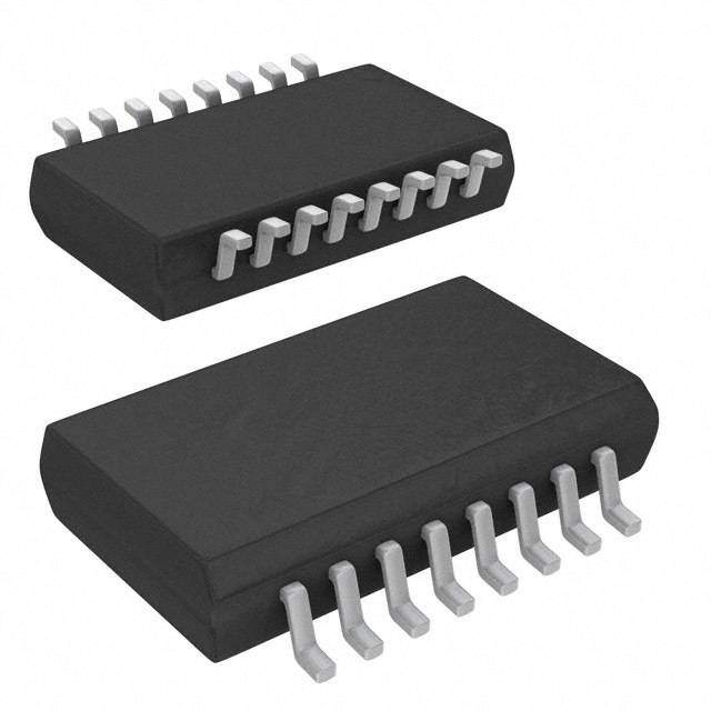
| 描述 | IC CURR-FDBK AMP VIDEO HS 16SOIC视频放大器 HI-Spd VIDEO IC |
| 产品分类 | |
| 品牌 | Analog Devices |
| 产品手册 | |
| 产品图片 |
|
| rohs | 否不符合限制有害物质指令(RoHS)规范要求 |
| 产品系列 | 放大器 IC,视频放大器,Analog Devices AD811AR-16- |
| 数据手册 | |
| 产品型号 | AD811AR-16 |
| 产品种类 | 视频放大器 |
| 供应商器件封装 | 16-SOIC W |
| 关闭 | No |
| 其它名称 | AD811AR16 |
| 包装 | 管件 |
| 压摆率 | 2500 V/µs |
| 双重电源电压 | +/- 5 V, +/- 15 V |
| 商标 | Analog Devices |
| 安装类型 | 表面贴装 |
| 安装风格 | SMD/SMT |
| 封装 | Tube |
| 封装/外壳 | 16-SOIC(0.295",7.50mm 宽) |
| 封装/箱体 | SOIC-16 |
| 工厂包装数量 | 47 |
| 应用 | 电流反馈 |
| 放大器类型 | Current Feedback Amplifier |
| 最大双重电源电压 | +/- 18 V |
| 最大工作温度 | + 85 C |
| 最小双重电源电压 | +/- 4.5 V |
| 最小工作温度 | - 40 C |
| 标准包装 | 47 |
| 电压-电源,单/双 (±) | ±4.5 V ~ 18 V |
| 电流-电源 | 16.5mA |
| 电流-输出/通道 | 100mA |
| 电源类型 | Dual |
| 电路数 | 1 |
| 系列 | AD811 |
| 转换速度 | 2500 V/us |
| 输入偏压电流—最大 | 10 uA |
| 输入补偿电压 | 3 mV |
| 输出类型 | No |
| 通道数量 | 1 Channel |


- 商务部:美国ITC正式对集成电路等产品启动337调查
- 曝三星4nm工艺存在良率问题 高通将骁龙8 Gen1或转产台积电
- 太阳诱电将投资9.5亿元在常州建新厂生产MLCC 预计2023年完工
- 英特尔发布欧洲新工厂建设计划 深化IDM 2.0 战略
- 台积电先进制程称霸业界 有大客户加持明年业绩稳了
- 达到5530亿美元!SIA预计今年全球半导体销售额将创下新高
- 英特尔拟将自动驾驶子公司Mobileye上市 估值或超500亿美元
- 三星加码芯片和SET,合并消费电子和移动部门,撤换高东真等 CEO
- 三星电子宣布重大人事变动 还合并消费电子和移动部门
- 海关总署:前11个月进口集成电路产品价值2.52万亿元 增长14.8%


PDF Datasheet 数据手册内容提取
High Performance Video Op Amp Data Sheet AD811 FEATURES CONNECTION DIAGRAMS High speed NC 1 8 NC 140 MHz bandwidth (3 dB, G = +1) –IN 2 7 +VS 1322550 0M 0MH VHz/ µzb sba snalndedwww irdiadtthteh (0 (.31 d dBB, ,G G = = + +22)) –+VINSN34C = ANOD 8C1O1NNE65CTONCUTPUT 00866-E-001 25 ns settling time to 0.1% (for a 2 V step) Figure 1. 8-Lead Plastic (N-8), CERDIP (Q-8), SOIC_N (R-8) 65 ns settling time to 0.01% (for a 10 V step) Excellent video performance (RL =150 Ω) NC 1 AD811 16 NC 0.01% differential gain, 0.01° differential phase NC 2 15 NC Voltage noise of 1.9 nV/√Hz –IN 3 14 +VS NC 4 13 NC Low distortion: THD = −74 dB at 10 MHz +IN 5 12 OUTPUT Excellent dc precision: 3 mV max input offset voltage NC 6 11 NC FleSxpibecleif oiepde froart i±o5n V and ±15 V operation –NVCS 78 (NToOt Pto V SIEcWale) 190 NNCC 00866-E-002 ±2.3 V output swing into a 75 Ω load (V = ±5 V) S NOTES APPLICATIONS 1. NC = NO CONNECT. DO NOT CONNECTTO THIS PIN. Figure 2. 16-Lead SOIC_W (RW-16) Video crosspoint switchers, multimedia broadcast systems C C C C C HDTV compatible systems N N N N N 3 2 1 20 19 Video line drivers, distribution amplifiers ADC/DAC buffers NC4 18NC NC5 AD811 17NC DC restoration circuits –IN6 16+VS Medical NC7 15NC UPEltTr a sound +IN8 (NToOt Pto V SIEcWale) 14OUTPUT 00866-E-003 Gamma 9 10 11 12 13 SC C C C Counter applications –V N N N N NOTES MIL-STD-883B parts available 1. NC = NO CONNECT. DO NOT CONNECTTO THIS PIN. Figure 3. 20-Terminal LCC (E-20-1) GENERAL DESCRIPTION A wideband current feedback operational amplifier, the AD811 The AD811 is also excellent for pulsed applications where is optimized for broadcast-quality video systems. The −3 dB transient response is critical. It can achieve a maximum slew bandwidth of 120 MHz at a gain of +2 and the differential gain rate of greater than 2500 V/µs with a settling time of less than and phase of 0.01% and 0.01° (R = 150 Ω) make the AD811 an 25 ns to 0.1% on a 2 V step and 65 ns to 0.01% on a 10 V step. L excellent choice for all video systems. The AD811 is designed to The AD811 is ideal as an ADC or DAC buffer in data acquisition meet a stringent 0.1 dB gain flatness specification to a bandwidth of systems due to its low distortion up to 10 MHz and its wide unity 35 MHz (G = +2) in addition to low differential gain and phase gain bandwidth. Because the AD811 is a current feedback ampli- errors. This performance is achieved whether driving one or two fier, this bandwidth can be maintained over a wide range of back-terminated 75 Ω cables, with a low power supply current gains. The AD811 also offers low voltage and current noise of of 16.5 mA. Furthermore, the AD811 is specified over a power 1.9 nV/√Hz and 20 pA/√Hz, respectively, and excellent dc supply range of ±4.5 V to ±18 V. accuracy for wide dynamic range applications. Rev. G Document Feedback Information furnished by Analog Devices is believed to be accurate and reliable. However, no responsibility is assumed by Analog Devices for its use, nor for any infringements of patents or other One Technology Way, P.O. Box 9106, Norwood, MA 02062-9106, U.S.A. rights of third parties that may result from its use. Specifications subject to change without notice. No license is granted by implication or otherwise under any patent or patent rights of Analog Devices. Tel: 781.329.4700 ©2015 Analog Devices, Inc. All rights reserved. Trademarks and registered trademarks are the property of their respective owners. Technical Support www.analog.com
AD811 Data Sheet TABLE OF CONTENTS Features .............................................................................................. 1 Typical Performance Characteristics ..............................................6 Applications ....................................................................................... 1 Applications Information .............................................................. 12 Connection Diagrams ...................................................................... 1 General Design Considerations ............................................... 12 General Description ......................................................................... 1 Achieving the Flattest Gain Response at High Frequency .... 12 Revision History ............................................................................... 2 Operation as a Video Line Driver ............................................ 14 Specifications ..................................................................................... 3 An 80 MHz Voltage-Controlled Amplifier Circuit................ 15 Absolute Maximum Ratings ............................................................ 5 A Video Keyer Circuit ............................................................... 16 Maximum Power Dissipation ..................................................... 5 Outline Dimensions ....................................................................... 18 Metalization Photograph ............................................................. 5 Ordering Guide .......................................................................... 20 ESD Caution .................................................................................. 5 REVISION HISTORY 4/15—Rev. F to Rev. G Changes to Figure 25 ........................................................................ 9 Changes to Ordering Guide .......................................................... 20 2/14—Rev. E to Rev. F Changes to R-8 Package, RW-16 Package, and E-20-1 Package; Deleted R-20 Package .................................................... Throughout Changes to Applications Section .................................................... 1 Removed Figure 4; Renumbered Sequentially .............................. 1 Moved Figure 4 and Figure 5 .......................................................... 6 Changes to An 80 MHz Voltage-Controlled Amplifier Circuit Section ................................................................................ 15 Updated Outline Dimensions, Removed Figure 54 ................... 18 Changes to Ordering Guide .......................................................... 19 7/04—Rev. D to Rev. E Updated Format .................................................................. Universal Change to Maximum Power Dissipation Section ........................ 7 Changes to Ordering Guide .......................................................... 20 Updated Outline Dimensions ....................................................... 20 Rev. G | Page 2 of 20
Data Sheet AD811 SPECIFICATIONS At T = +25°C, V = ±15 V dc, R = 150 Ω, unless otherwise noted. A S LOAD Table 1. AD811J/AD811A1 AD811S2 Parameter Conditions V Min Typ Max Min Typ Max Unit S DYNAMIC PERFORMANCE Small Signal Bandwidth (No Peaking) −3 dB G = +1 R = 562 Ω ±15 V 140 140 MHz FB G = +2 R = 649 Ω ±15 V 120 120 MHz FB G = +2 R = 562 Ω ±15 V 80 80 MHz FB G = +10 R = 511 Ω ±15 V 100 100 MHz FB 0.1 dB Flat G = +2 R = 562 Ω ±15 25 25 MHz FB R = 649 Ω ±15 35 35 MHz FB Full Power Bandwidth3 V = 20 V p-p ±15 40 40 MHz OUT Slew Rate V = 4 V p-p ±15 400 400 V/µs OUT V = 20 V p-p ±15 2500 2500 V/µs OUT Settling Time to 0.1% 10 V Step, A = − 1 ±15 50 50 ns V Settling Time to 0.01% 10 V Step, A = − 1 ±15 65 65 ns V Settling Time to 0.1% 2 V Step, A = − 1 ±15 25 25 ns V Rise Time, Fall Time R = 649, A = +2 ±15 3.5 3.5 ns FB V Differential Gain f = 3.58 MHz ±15 0.01 0.01 % Differential Phase f = 3.58 MHz ±15 0.01 0.01 Degree THD at f = 10 MHz V = 2 V p-p, A = +2 ±15 −74 −74 dBc C OUT V Third-Order Intercept4 At f = 10 MHz ±15 36 36 dBm C ±15 43 43 dBm INPUT OFFSET VOLTAGE ±5 V, ±15 V 0.5 3 0.5 3 mV T to T 5 5 mV MIN MAX Offset Voltage Drift 5 5 µV/°C INPUT BIAS CURRENT −Input ±5 V, ±15 V 2 5 2 5 µA T to T 15 30 µA MIN MAX +Input ±5 V, ±1 5 V 2 10 2 10 µA T to T 20 25 µA MIN MAX TRANSRESISTANCE T to T MIN MAX V = ±10 V OUT R = ∞ ±15 V 0.75 1.5 0.75 1.5 MΩ L R = 200 Ω ±15 V 0.5 0.75 0.5 0.75 MΩ L V = ±2.5 V OUT R = 150 Ω ±5 V 0.25 0.4 0.125 0.4 MΩ L COMMON-MODE REJECTION V (vs. Common Mode) OS T to T V = ±2.5 V ±5 V 56 60 50 60 dB MIN MAX CM T to T V = ±10 V ±15 V 60 66 56 66 dB MIN MAX CM Input Current (vs. Common Mode) T to T 1 3 1 3 µA/V MIN MAX POWER SUPPLY REJECTION V = ±4.5 V to ±18 V S V T to T 60 70 60 70 dB OS MIN MAX +Input Current T to T 0.3 2 0.3 2 µA/V MIN MAX −Input Current T to T 0.4 2 0.4 2 µA/V MIN MAX Rev. G | Page 3 of 20
AD811 Data Sheet AD811J/AD811A1 AD811S2 Parameter Conditions V Min Typ Max Min Typ Max Unit S INPUT VOLTAGE NOISE f = 1 kHz 1.9 1.9 nV/√Hz INPUT CURRENT NOISE f = 1 kHz 20 20 pA/√Hz OUTPUT CHARACTERISTICS Voltage Swing, Useful Operating ±5 V ±2.9 ±2.9 V Range5 ±15 V ±12 ±12 V Output Current T = 25°C 100 100 mA J Short-Circuit Current 150 150 mA Output Resistance (Open Loop at 5 MHz) 9 9 Ω INPUT CHARACTERISTIC +Input Resistance 1.5 1.5 MΩ −Input Resistance 14 14 Ω Input Capacitance +Input 7.5 7.5 pF Common-Mode Voltage Range ±5 V ±3 ±3 V ±15 V ±13 ±13 V POWER SUPPLY Operating Range ±4.5 ±18 ±4.5 ±18 V Quiescent Current ±5 V 14.5 16.0 14.5 16.0 mA ±15 V 16.5 18.0 16.5 18.0 mA TRANSISTOR COUNT Number of Transistors 40 40 1 The AD811JR is specified with ±5 V power supplies only, with operation up to ±12 V. 2 See the Analog Devices military data sheet for 883B tested specifications. 3 FPBW = slew rate/(2 π VPEAK). 4 Output power level, tested at a closed-loop gain of two. 5 Useful operating range is defined as the output voltage at which linearity begins to degrade. Rev. G | Page 4 of 20
Data Sheet AD811 ABSOLUTE MAXIMUM RATINGS MAXIMUM POWER DISSIPATION Table 2. The maximum power that can be safely dissipated by the AD811 is Parameter Rating limited by the associated rise in junction temperature. For the Supply Voltage ±18 V plastic packages, the maximum safe junction temperature is 145°C. AD811JR Grade Only ±12 V For the CERDIP and LCC packages, the maximum junction tem- Internal Power Dissipation Observe Derating Curves perature is 175°C. If these maximums are exceeded momentarily, 8-Lead PDIP Package θ = 90°C/ W JA proper circuit operation is restored as soon as the die tempera- 8-Lead CERDIP Package θ = 110°C/W JA ture is reduced. Leaving the device in the overheated condition 8-Lead SOIC_N Package θ = 155°C/W JA for an extended period can result in device burnout. To ensure 16-Lead SOIC_W Package θ = 85°C/W JA proper operation, it is important to observe the derating curves 20-Lead LCC Package θ = 70°C/W JA in Figure 21 and Figure 24. Output Short-Circuit Duration Observe Derating Curves Common-Mode Input Voltage ±V While the AD811 is internally short-circuit protected, this may S Differential Input Voltage ±6 V not be sufficient to guarantee that the maximum junction tem- Storage Temperature Range (Q, E) −65°C to +150°C perature is not exceeded under all conditions. An important Storage Temperature Range (N, R) −65°C to +125°C example is when the amplifier is driving a reverse-terminated Operating Temperature Range 75 Ω cable and the cable’s far end is shorted to a power supply. AD811J 0°C to +70°C With power supplies of ±12 V (or less) at an ambient temperature AD811A −40°C to +85°C of +25°C or less, and the cable shorted to a supply rail, the AD811S −55°C to +125°C amplifier is not destroyed, even if this condition persists for Lead Temperature Range 300°C an extended period. (Soldering 60 sec) METALIZATION PHOTOGRAPH Stresses at or above those listed under Absolute Maximum Contact the factory for the latest dimensions. Ratings may cause permanent damage to the product. This is a stress rating only; functional operation of the product at these V+ VOUT 7 6 or any other conditions above those indicated in the operational section of this specification is not implied. Operation beyond the maximum operating conditions for extended periods may affect product reliability. 0.0618 (1.57) –INPUT 2 0.098 (2.+4I9N)P3UTAD811 V4– 00866-E-007 Figure 4. Metalization Photograph Dimensions Shown in Inches and (Millimeters) ESD CAUTION Rev. G | Page 5 of 20
AD811 Data Sheet TYPICAL PERFORMANCE CHARACTERISTICS 0.10 0.20 35 RF = 649Ω 0.09 FC = 3.58MHz 0.18 100 IRE S) 30 0.08 MODULATED RAMP 0.16 E L GAIN (%) 00..0067 RL = 150Ω 00..1124 ASE (DEGRE AGE (V p-p) 2205 VS =±15V DIFFERENTIA 000...000345 PHASE 000...001680 ERENTIAL PH OUTPUT VOLT 1105 0.02 GAIN 0.04 DIFF 5 VS =±5V 0.01 0.02 05 6 7 8SUPP9LY VO10LTAG1E1 (±V1)2 13 14 150 00866-E-005 010 1L0O0AD RESISTANCE (1Ωk) 10k 00866-E-009 Figure 5. Differential Gain and Phase Figure 8. Output Voltage Swing vs. Resistive Load 12 10 9 GRL = = + 1250Ω Hz) 5 NONIN±V5 ETROT±IN1G5V INPUT RG = RFB Y (M 0 6 VS =±15V UENC –5 VS =±5V N (dB) 3 VS =±5V FREQ –10 INVERTING INPUT AI K G OC VS =±15V L –15 0 C R TE –20 S –3 MA –25 –61 FREQ10UENCY (MHz) 100 00866-E-006 –30–60 –40 –20 JU0NCTIO2N0 TEM40PERA6T0URE8 (0°C) 100 120 140 00866-E-010 Figure 6. Frequency Response Figure 9. Input Bias Current vs. Junction Temperature 20 20 V) NGE (±V) 15 TA = 25°C LTAGE (± 15 TA = 25°C A O R V E T AG PU RL = 150Ω LT UT O 10 O 10 E V HE OD F T NO LOAD M O N- E MO 5 UD 5 COM AGNIT M 00 5 SUPPLY V1O0LTAGE (±V) 15 20 00866-E-008 00 5 SUPPLY V1O0LTAGE (±V) 15 20 00866-E-011 Figure 7. Input Common-Mode Voltage Range vs. Supply Voltage Figure 10. Output Voltage Swing vs. Supply Voltage Rev. G | Page 6 of 20
Data Sheet AD811 21 10 Ω) mA) 18 CE ( NT ( VS =±15V TAN E S Y CURR 15 UT RESI 1 VS =±15V ENT SUPPL 129 VS =±5V OOP OUTP 0.1 VS =±5V SC D-L E E QUI 6 OS GAIN =–2 CL RFB = 649Ω 3–60 –40 –20 JU0NCTIO2N0 TEM40PERA6T0URE8 (0°C) 100 120 140 00866-E-012 0.0110k 100k FREQU1EMNCY (Hz) 10M 100M 00866-E-015 Figure 11. Quiescent Supply Current vs. Junction Temperature Figure 14. Closed-Loop Output Resistance vs. Frequency 10 10 100 8 RISE TIME V) 6 8 60 m E ( 4 OFFSET VOLTAG –202 VS =±15V VS =±5V RISE TIME (ns) 46 OVERSHOOT VVRGSOLA I===N ±11 =15V 50+ pVΩ2-p 2400 OVERSHOOT (%) T –4 U P IN –6 2 0 –8 –10–60 –40 –20 JU0NCTIO2N0 TEM40PERA6T0URE8 (0°C) 100 120 140 00866-E-013 00.4 0V.A6LUE OF0 F.8EEDBAC1K.0 RESISTO1.R2 [RFB] (k1Ω.4) 1.6–20 00866-E-016 Figure 12. Input Offset Voltage vs. Junction Temperature Figure 15. Rise Time and Overshoot vs. Value of Feedback Resistor, RFB 250 2.0 VS =±15V A) RL = 200Ω T CURRENT (m 125000 VS =±15V ΩSTANCE (M) 11..50 VOUT =±10V UI SI RT-CIRC VS =±5V RANSRE VRVSOL U==T ±1 =55V0±Ω2.5V O 100 T 0.5 H S 50–60 –40 –20 JU0NCTIO2N0 TEM40PERA6T0URE8 (0°C) 100 120 140 00866-E-014 0–60 –40 –20 JU0NCTIO2N0 TEM40PERA6T0URE8 (0°C) 100 120 140 00866-E-017 Figure 13. Short-Circuit Current vs. Junction Temperature Figure 16. Transresistance vs. Junction Temperature Rev. G | Page 7 of 20
AD811 Data Sheet 100 100 80 70 RF = 649Ω AV = +2 V/ Hz) NONINVERTING CURRENT VS =±5V TO±15V A/ Hz) 60 VS =±5V E VOLTAGE (n 10 INVERTING CURRENT VS =±5V TO±15V 10 E CURRENT (p PSRR (dB) 345000 CCOUANRSEEV S ECUSOP APNRLDYEIT IFISOO NVRA WWRHIOEERDRSET VS =±15V S S WHILE THE OTHER IS NOI NOI 20 HELD CONSTANT. VOLTAGE NOISE VS =±15V 10 VOLTAGE NOISE VS =±5V 110 100 FREQUE1kNCY (Hz) 10k 100k1 00866-E-018 51k 10k FREQU1E00NkCY (Hz) 1M 10M 00866-E-021 Figure 17. Input Noise vs. Frequency Figure 20. Power Supply Rejection Ration vs. Frequency 200 10 2.5 TJ MAX = –145°C 16-LEAD SOIC 160 8 W) Hz) ON ( 2.0 B BANDWIDTH (M 12800 BANDWIDTH VVRGSOLA I===N ±11 =15V 50+ pVΩ2-p 46 PEAKING (dB) OWER DISSIPATI 1.5 8-LEAD PDIP –3d PEAKING TAL P 1.0 40 2 O 8-LEAD SOIC T 00.4 0V.A6LUE OF0 F.8EEDBAC1K.0 RESISTO1.R2 [RFB] (k1Ω.4) 1.60 00866-E-019 0.5–50 –40 –30 –20 –A1M0BIE0NT 1T0EM2P0ER3A0TU4R0E (°5C0) 60 70 80 90 00866-E-022 Figure 18. −3 dB Bandwidth and Peaking vs. Value of RFB Figure 21. Maximum Power Dissipation vs. Temperature for Plastic Packages 110 25 649Ω 100 649Ω VS =±15V VIN VOUT 20 90 p) B) 80 150Ω 150Ω GE (V p- 15 GOAUITNP =U T+ 1L0EVEL d A FOR 3% THD R ( 70 LT R O M VS =±15V V C T 10 60 U P VS =±5V UT 50 O 5 VS =±5V 40 301k 10k FREQU1E00NkCY (Hz) 1M 10M 00866-E-020 0100k 1MFREQUENCY (Hz)10M 100M 00866-E-023 Figure 19. Common-Mode Rejection Ratio vs. Frequency Figure 22. Large Signal Frequency Response Rev. G | Page 8 of 20
Data Sheet AD811 –50 RL = 100Ω ±5V SUPPLIES 1V 10ns VOUT = 2V p-p GAIN = +2 c) 100 dB�–70 SECOND HARMONIC VIN 90 N ( O TI R O ST –90 DI C THIRD HARMONIC NI O HARM–110 ±15V SUPPLIES VOUT 100% SECOND HARMONIC 1V THIRD HARMONIC –1301k 10k FREQU1E00NkCY (Hz) 1M 10M 00866-E-024 00866-E-027 Figure 23. Harmonic Distortion vs. Frequency Figure 26. Small Signal Pulse Response, Gain = +1 3.4 3.2 TJ MAX =–175°C 100mV 10ns 3.0 W) 2.8 100 ON ( 2.6 VIN 90 TI 2.4 A SIP 2.2 20-LEAD LCC DIS 2.0 R 1.8 E W 1.6 8-LEAD CERDIP O P 1.4 AL 1.2 VOUT 10 T TO 1.0 0% 0.8 1V 0.6 0.4–60 –40 –20 AM0BIEN2T0 TEM4P0ERA6T0URE 8(°0C) 100 120 140 00866-E-025 00866-E-028 Figure 24. Maximum Power Dissipation vs. Figure 27. Small Signal Pulse Response, Gain = +10 Temperature for Hermetic Packages 9 G = +1 RFB 6 RRLG == 1∞50Ω +VS 3 VOUT TO VS =±15V RG 2 – 7 0.1µF TPPE6R2KO0TB1R EFOENTIX N (dB) 0 RFB = 750Ω AI AD811 6 G –3 VHPIUPN8L1S3E0 50Ω 3 + 4 RL –6 VRSF B= =± 56V19Ω GENERATOR –9 0.1µF –VS 00866-026 –121 FREQ10UENCY (MHz) 100 00866-E-029 Figure 25. Noninverting Amplifier Connection Figure 28. Closed-Loop Gain vs. Frequency, Gain = +1 Rev. G | Page 9 of 20
AD811 Data Sheet 26 G = +1 1V 10ns 23 RL = 150Ω 100 VS =±15V VIN 90 20 RFB = 511Ω B) d N ( 17 AI G VS =±5V 14 RFB = 442Ω VOUT 10 0% 11 1V 81 FREQ10UENCY (MHz) 100 00866-E-030 00866-E-033 Figure 29. Closed-Loop Gain vs. Frequency, Gain = +10 Figure 32. Small Signal Pulse Response, Gain = −1 1V 20ns 100mV 10ns 100 100 VIN 90 VIN 90 VOUT 10 VOUT 10 0% 0% 10V 1V 00866-E-031 00866-E-034 Figure 30. Large Signal Pulse Response, Gain = +10 Figure 33. Small Signal Pulse Response, Gain = −10 RFB 6 G =–1 +VS 3 RL = 150Ω VS =±15V 0.1µF VOUT TO 0 RFB = 590Ω VIN RG 2 – 7 TPPE6R2KO0TB1RE FOENTIX dB) HP8130 N ( –3 PULSE AD811 6 AI GENERATOR G 3 + 4 RL –6 VRSF B= =± 55V62Ω –9 0.1µF –VS 00866-E-032 –121 FREQ10UENCY (MHz) 100 00866-E-035 Figure 31. Inverting Amplifier Connection Figure 34. Closed-Loop Gain vs. Frequency, Gain = −1 Rev. G | Page 10 of 20
Data Sheet AD811 26 G =–1 1V 20ns 23 RL = 150Ω 100 VIN 90 VS =±15V 20 RFB = 511Ω B) d N ( 17 AI G VS =±5V 14 RFB = 442Ω VOUT 10 0% 11 10V 81 FREQ10UENCY (MHz) 100 00866-E-036 00866-E-037 Figure 35. Closed-Loop Gain vs. Frequency, Gain = −10 Figure 36. Large Signal Pulse Response, Gain = −10 Rev. G | Page 11 of 20
AD811 Data Sheet APPLICATIONS INFORMATION GENERAL DESIGN CONSIDERATIONS ACHIEVING THE FLATTEST GAIN RESPONSE AT HIGH FREQUENCY The AD811 is a current feedback amplifier optimized for use in high performance video and data acquisition applications. Achieving and maintaining gain flatness of better than 0.1 dB at Because it uses a current feedback architecture, its closed-loop frequencies above 10 MHz requires careful consideration of −3 dB bandwidth is dependent on the magnitude of the several issues. feedback resistor. The desired closed-loop gain and bandwidth Choice of Feedback and Gain Resistors are obtained by varying the feedback resistor (R ) to tune the FB Because of the previously mentioned relationship between the bandwidth and by varying the gain resistor (R ) to obtain the G 3 dB bandwidth and the feedback resistor, the fine scale gain correct gain. Table 3 contains recommended resistor values for flatness varies, to some extent, with feedback resistor tolerance. a variety of useful closed-loop gains and supply voltages. Therefore, it is recommended that resistors with a 1% tolerance Table 3. −3 dB Bandwidth vs. Closed-Loop Gain and be used if it is desired to maintain flatness over a wide range of Resistance Values production lots. In addition, resistors of different construction V = ±15 V have different associated parasitic capacitance and inductance. S Closed-Loop Gain R R −3 dB BW (MHz) Metal film resistors were used for the bulk of the character- FB G +1 750 Ω 140 ization for this data sheet. It is possible that values other than +2 649 Ω 649 Ω 120 those indicated are optimal for other resistor types. +10 511 Ω 56.2 Ω 100 Printed Circuit Board Layout Considerations −1 590 Ω 590 Ω 115 As is expected for a wideband amplifier, PC board parasitics can −10 511 Ω 51.1 Ω 95 affect the overall closed-loop performance. Of concern are stray V = ±5 V S capacitances at the output and the inverting input nodes. If a Closed-Loop Gain R R −3 dB BW (MHz) FB G ground plane is used on the same side of the board as the signal +1 619 Ω 80 traces, a space (3/16" is plenty) should be left around the signal +2 562 Ω 562 Ω 80 lines to minimize coupling. Additionally, signal lines connecting +10 442 Ω 48.7 Ω 65 the feedback and gain resistors should be short enough so that −1 562 Ω 562 Ω 75 their associated inductance does not cause high frequency gain −10 442 Ω 44.2 Ω 65 errors. Line lengths less than 1/4" are recommended. V = ±10 V S Quality of Coaxial Cable Closed-Loop Gain R R −3 dB BW (MHz) FB G +1 649 Ω 105 Optimum flatness when driving a coax cable is possible only +2 590 Ω 590 Ω 105 when the driven cable is terminated at each end with a resistor +10 499 Ω 49.9 Ω 80 matching its characteristic impedance. If the coax is ideal, then −1 590 Ω 590 Ω 105 the resulting flatness is not affected by the length of the cable. −10 499 Ω 49.9 Ω 80 While outstanding results can be achieved using inexpensive cables, note that some variation in flatness due to varying cable lengths may occur. Figure 17 and Figure 18 illustrate the relationship between the Power Supply Bypassing feedback resistor and the frequency and time domain response characteristics for a closed-loop gain of +2. (The response at Adequate power supply bypassing can be critical when optimiz- other gains is similar.) ing the performance of a high frequency circuit. Inductance in the power supply leads can form resonant circuits that produce The 3 dB bandwidth is somewhat dependent on the power peaking in the amplifier’s response. In addition, if large current supply voltage. As the supply voltage is decreased, for example, transients must be delivered to the load, then bypass capacitors the magnitude of the internal junction capacitances is increased, (typically greater than 1 µF) are required to provide the best causing a reduction in closed-loop bandwidth. To compensate settling time and lowest distortion. Although the recommended for this, smaller values of feedback resistor are used at lower 0.1 µF power supply bypass capacitors are sufficient in many supply voltages. applications, more elaborate bypassing (such as using two paralleled capacitors) may be required in some cases. Rev. G | Page 12 of 20
Data Sheet AD811 Driving Capacitive Loads 100 GAIN = +2 The feedback and gain resistor values in Table 3 result in very 90 VS =±15V RS VALUE SPECIFIED flat closed-loop responses in applications where the load 80 IS FOR FLATTEST FREQUENCY RESPONSE capacitances are below 10 pF. Capacitances greater than this 70 result in increased peaking and overshoot, although not Ω ()S 60 R necessarily in a sustained oscillation. F O 50 E There are at least two very effective ways to compensate for this U L 40 A effect. One way is to increase the magnitude of the feedback V 30 resistor, which lowers the 3 dB frequency. The other method is 20 to include a small resistor in series with the output of the ampli- fier to isolate it from the load capacitance. The results of these 10 tfdewreiodv ibtneagcch k1n 0ri0eqs upiseFts.o Tar,rh eteh i elml uoasuitntrpa duteitsd ar idipnvp aFlneig tiausg rleee s o3sf8 tt.h hUainss i mn0.ge5 ta hd 1oB.d 5w ikhsΩ ethn a t it 010 LOAD CAPA10C0ITANCE (pF) 1000 00866-E-040 Figure 39. Recommended Value of Series Resistor vs. sacrifices a little bit of gain flatness for increased capacitive load the Amount of Capacitive Load drive capability. With the second method, using a series resistor, the loss of flatness does not occur. Figure 39 shows recommended resistor values for different load capacitances. Refer again to Figure 38 for an example of the RFB results of this method. Note that it may be necessary to adjust +VS the gain setting resistor, RG, to correct for the attenuation which results due to the divider formed by the series resistor, R, and S 0.1µF the load resistance. RG 2 – 7 Applications that require driving a large load capacitance at a RS (OPTIONAL) high slew rate are often limited by the output current available AD811 6 VOUT VIN from the driving amplifier. For example, an amplifier limited to 3 + 4 CL RL 25 mA output current cannot drive a 500 pF load at a slew rate RT greater than 50 V/µs. However, because of the 100 mA output 0.1µF current of the AD811, a slew rate of 200 V/µs is achievable when driving the same 500 pF capacitor, as shown in Figure 40. –VS 00866-E-038 2V 100ns Figure 37. Recommended Connection for Driving a Large Capacitive Load 100 12 VIN 90 9 RFB = 1.5kΩ RS = 0 6 B) AIN (d 3 RRFSB = = 3 604Ω9Ω VOUT 100% G 0 VRCSLL === ±1110050kVpΩF 5V –3 GAIN = +2 00866-E-041 Figure 40. Output Waveform of an AD811 Driving a 500 pF Load. –61 FREQ10UENCY (MHz) 100 00866-E-039 Gain = +2, RFB = 649 Ω, RS = 15 Ω, RS = 10 kΩ Figure 38. Performance Comparison of Two Methods for Driving a Capacitive Load Rev. G | Page 13 of 20
AD811 Data Sheet OPERATION AS A VIDEO LINE DRIVER 1V 10ns The AD811 has been designed to offer outstanding performance at closed-loop gains of +1 or greater, while driving multiple 100 VIN 90 reverse-terminated video loads. The lowest differential gain and phase errors are obtained when using ±15 V power supplies. With ±12 V supplies, there is an insignificant increase in these errors and a slight improvement in gain flatness. Due to power dissipation considerations, ±12 V supplies are recommended for optimum video performance. Excellent performance can be VOUT 10 achieved at much lower supplies as well. 0% 1V The closed-loop gain versus the frequency at different supply vpohlotatoggersa ips hsh oofw ann iAnD F8ig1u1r lein 4e2 .d Friivgeurr’se p4u3l sise arnes opsocnilsleo swciotphe 00866-E-044 ±15 V supplies. The differential gain and phase error versus the Figure 43. Small Signal Pulse Response, Gain = +2, VS = ±15 V supply are plotted in Figure 44 and Figure 45, respectively. 0.10 Another important consideration when driving multiple cables RF = 649Ω 0.09 FC = 3.58MHz is the high frequency isolation between the outputs of the 100 IRE 0.08 MODULATED RAMP cables. Due to its low output impedance, the AD811 achieves better than 40 dB of output-to-output isolation at 5 MHz N (%) 0.07 driving back-terminated 75 Ω cables. GAI 0.06 L 649Ω 649Ω 75Ω CABLE TIA 0.05 75Ω VOUT No. 1 REN 0.04 +VS 75Ω DIFFE 0.03 a b . . DTDERRRIIVVMIINNINGGA ATTWE SDOIN, 7PG5ALΩRE ,AC BLOALAECXLK C,- BAABCLKE- 0.1µF 0.02 TERMINATED, COAX CABLES b 7 0.01 a 2 – VIN75Ω CABLE 3 + AD811 6 75Ω75Ω CABLE75ΩVOUT No. 2 05 6 7 8SUP9PLY V1O0LTA1G1E (V)12 13 14 15 00866-E-045 4 Figure 44. Differential Gain Error vs. Supply Voltage for 75Ω the Video Line Driver of Figure 41 0.1µF 0.20 –VS 00866-E-042 EES) 00..1168 RF1M0CFO0 ==D I RU36.4EL59A8ΩMTEHDz RAMP R Figure 41. A Video Line Driver Operating at a Gain of +2 EG 0.14 D b 12 SE ( 0.12 A H 0.10 9 RGRLG = = =+ 12R5F0BΩ NTIAL P 0.08 a a b . . DTDERRRIIVVMIINNINGGA ATTWE SDOIN, 7PG5ALΩRE ,AC BLOALAECXLK C,- BAABCLKE- 6 VRSF B= =± 1654V9Ω FERE 0.06 TERMINATED, COAX CABLES F 0.04 B) DI d AIN ( 3 VRSF B= =± 55V62Ω 0.02 G 0 05 6 7 8SUP9PLY V1O0LTA1G1E (V)12 13 14 15 00866-E-046 Figure 45. Differential Phase Error vs. Supply Voltage for –3 the Video Line Driver of Figure 41 –61 FREQ10UENCY (MHz) 100 00866-E-043 Figure 42. Closed-Loop Gain vs. Frequency, Gain = +2 Rev. G | Page 14 of 20
Data Sheet AD811 AN 80 MHZ VOLTAGE-CONTROLLED AMPLIFIER The gain can be increased to 20 dB (×10) by raising R8 and R9 CIRCUIT to 1.27 kΩ, with a corresponding decrease in −3 dB bandwidth to approximately 25 MHz. The maximum output voltage under The voltage-controlled amplifier (VCA) circuit of Figure 46 shows these conditions is increased to ±9 V using ±12 V supplies. the AD811 being used with the AD834, a 500 MHz, 4-quadrant multiplier. The AD834 multiplies the signal input by the dc control The gain-control input voltage, VG, may be a positive or negative voltage, V . The AD834 outputs are in the form of differential ground-referenced voltage, or fully differential, depending on G currents from a pair of open collectors, ensuring that the full the choice of connections at Pin 7 and Pin 8. A positive value of bandwidth of the multiplier (which exceeds 500 MHz) is VG results in an overall noninverting response. Reversing the sign available for certain applications. Here, the AD811 op amp of VG simply causes the sign of the overall response to invert. In provides a buffered, single-ended, ground-referenced output. fact, although this circuit has been classified as a voltage-controlled Using feedback resistors R8 and R9 of 511 Ω, the overall gain amplifier, it is also quite useful as a general-purpose, four-quadrant ranges from −70 dB for V = 0 V to +12 V (a numerical gain of multiplier, with good load driving capabilities and fully G +4) when V = 1 V. The overall transfer function of the VCA is symmetrical responses from the X and Y inputs. G V = 4 (X1 − X2)(Y1 − Y2), which reduces to V = 4 V V OUT OUT G IN The AD811 and AD834 can both be operated from power supply using the labeling conventions shown in Figure 46. The circuit’s voltages of ±5 V. While it is not necessary to power them from −3 dB bandwidth of 80 MHz is maintained essentially constant— the same supplies, the common-mode voltage at W1 and W2 that is, independent of gain. The response can be maintained must be biased within the common-mode range of the input flat to within ±0.1 dB from dc to 40 MHz at full gain with the stage of the AD811. To achieve the lowest differential gain and addition of an optional capacitor of about 0.3 pF across the phase errors, it is recommended that the AD811 be operated feedback resistor R8. The circuit produces a full-scale output of from power supply voltages of ±10 V or greater. This VCA ±4 V for a ±1 V input and can drive a reverse-terminated load circuit operates from a ±12 V dual power supply. of 50 Ω or 75 Ω to ±2 V. FB +12V C1 0.1F + R1 100 R8* VG – R2 100 8 7 6 5 R4 R6 182 294 X2 X1 +VS W1 7 2 – ADU8134 ADU8311 6 VOUT 3 + 4 Y11 Y22 –3VS W42 182R5 294R7 RL VIN R9* R3 249 C2 0.1F FB *RR88 == RR99 == 15.1217k F OFROR4 1G0A GINAIN –12V 00866-E-047 Figure 46. An 80 MHz Voltage-Controlled Amplifier Rev. G | Page 15 of 20
AD811 Data Sheet A VIDEO KEYER CIRCUIT inverting input X2 while X1 is biased at an accurate 1 V. Thus, when V = 0, the response to video input V is already at its By using two AD834 multipliers, an AD811, and a 1 V dc source, G B full-scale value of unity, whereas when V = 1 V, the differential a special form of a two-input VCA circuit called a video keyer G input X1 − X2 is 0. This generates the second term. can be assembled. Keying is the term used in reference to blending two or more video sources under the control of a third signal or The bias currents required at the output of the multipliers are signals to create such special effects as dissolves and overlays. provided by R8 and R9. A dc level-shifting network comprising The circuit shown in Figure 47 is a two-input keyer, with video R10/R12 and R11/R13 ensures that the input nodes of the inputs V and V , and a control input V . The transfer function AD811 are positioned at a voltage within its common-mode A B G (with V at the load) is given by range. At high frequencies, C1 and C2 bypass R10 and R11, OUT respectively. R14 is included to lower the HF loop gain and is V = GV + (1 − G)V OUT A B needed because the voltage-to-current conversion in the where G is a dimensionless variable (actually, just the gain of the AD834s, via the Y2 inputs, results in an effective value of the A signal path) that ranges from 0 when V = 0 to 1 when V = G G feedback resistance of 250 Ω; this is only about half the value 1 V. Thus, V varies continuously between V and V as G OUT A B required for optimum flatness in the AD811’s response. (Note varies from 0 to 1. that this resistance is unaffected by G: when G = +1, all the Circuit operation is straightforward. Consider first the signal path feedback is via U1, while when G = 0 it is all via U2). R14 through U1, which handles video input V . Its gain is clearly 0 reduces the fractional amount of output current from the A when V = 0, and the scaling chosen ensures that it has a unity multipliers into the current-summing inverting input of the G value when V = 1 V; this takes care of the first term of the transfer AD811 by sharing it with R8. This resistor can be used to adjust G function. On the other hand, the V input to U2 is taken to the the bandwidth and damping factor to best suit the application. G +5V 0.C1µ1F SEER 1T4EXT SETUP FOR DRIVING REVERSE-TERMINATED LOAD R7 11R35Ω 45.3Ω 2.R491k0Ω TOA PDI8N1 61 ZO VOUT (V0G TO +1V dc) 22R66Ω 200Ω ZO TO Y2 8 7 6 5 200Ω X2 X1 +VS W1 +5V R1 U4 U1 R8 R12 INSET 1.87kΩ AD589 AD834 29.4Ω 6.98kΩ +5V 174RΩ2 Y1 Y2 –VS W2 1 2 3 4 FB VA (±1V FS) C3 –5V 0.1µF R3 +5V –5V LOAD 100Ω GND 7 2 – R4 8 7 6 5 2R99.4Ω 6R.1938kΩ ADU8311 6 VOUT 1.02kΩ X2 X1 +VS W1 3 + 4 C2 C4 U1 0.1µF 0.1µF AD834 Y1 Y2 –VS W2 FB LGONADD 1 2 3 4 VB (±1V FS) –5V 2.R491k1Ω –5V 00866-E-048 Figure 47. A Practical Video Keyer Circuit Rev. G | Page 16 of 20
Data Sheet AD811 To generate the 1 V dc needed for the 1 − G term, an AD589 R14 and 70 MHz with R14 = 49.9 Ω. For more information on reference supplies 1.225 V ± 25 mV to a voltage divider consisting the design and operation of the VCA and video keyer circuits, of resistors R2 through R4. Potentiometer R3 should be adjusted refer to the AN-216 Application Note, Video VCAs and Keyers: to provide exactly 1 V at the X1 input. Using the AD834 and AD811 by Brunner, Clarke, and Gilbert, available on the Analog Devices, Inc. website at www.analog.com. In this case, an arrangement is shown using dual supplies of ±5 V for both the AD834 and the AD811. Also, the overall gain is 10 R14 = 49.9Ω arranged to be unity at the load when it is driven from a reverse- 0 GAIN terminated 75 Ω line. This means that the dual VCA has to operate –10 R14 = 137Ω at a maximum gain of +2, rather than +4 as in the VCA circuit B) d –20 of Figure 46. However, this cannot be achieved by lowering the N ( AI –30 feedback resistor because below a critical value (not much less G P than 500 Ω) the peaking of the AD811 may be unacceptable. OO –40 L This is because the dominant pole in the open-loop ac response D- –50 E S ADJACENT CHANNEL of a current feedback amplifier is controlled by this feedback LO –60 FEEDTHROUGH C resistor. It would be possible to operate at a gain of ×4 and then –70 attenuate the signal at the output. Instead, the signals have been –80 attenuated by 6 dB at the input to the AD811; this is the fFuignucrtieo 4n8 o ifs Ra8 p tlohtr oouf gthhe R a1c1 r.e sponse of the feedback keyer when –9010k 100k FREQU1EMNCY (Hz) 10M 100M 00866-E-049 Figure 48. A Plot of the AC Response of the Video Keyer driving a reverse-terminated 50 Ω cable. Output noise and adjacent channel feedthrough, with either channel fully off and the other fully on, is about −50 dB to 10 MHz. The feedthrough at 100 MHz is limited primarily by board layout. For V = 1 V, G the −3 dB bandwidth is 15 MHz when using a 137 Ω resistor for Rev. G | Page 17 of 20
AD811 Data Sheet OUTLINE DIMENSIONS 0.400 (10.16) 0.365 (9.27) 0.355 (9.02) 8 5 0.280 (7.11) 0.250 (6.35) 1 4 0.240 (6.10) 0.325 (8.26) 0.310 (7.87) 0.100 (2.54) 0.300 (7.62) BSC 0.060 (1.52) 0.195 (4.95) 0.210 (5.33) MAX 0.130 (3.30) MAX 0.115 (2.92) 0.015 0.150 (3.81) (0.38) 0.015 (0.38) 0.130 (3.30) MIN GAUGE 0.115 (2.92) SEATING PLANE 0.014 (0.36) PLANE 0.010 (0.25) 0.022 (0.56) 0.008 (0.20) 0.005 (0.13) 0.430 (10.92) 0.018 (0.46) MIN MAX 0.014 (0.36) 0.070 (1.78) 0.060 (1.52) 0.045 (1.14) COMPLIANTTO JEDEC STANDARDS MS-001 CONTROLLING DIMENSIONSARE IN INCHES; MILLIMETER DIMENSIONS (RCINEOFRPEANRREEREN NLCTEEHA EODSNSEL MSY)AAAYNR BDEE AR CROOEU NNNFODIGETUDAR-POEPFDRFOA INSPC RWHIAH ETOEQL UFEIO VORAR LU EHSNAETL ISFN FLDOEEARSDIGSN.. 070606-A Figure 49. 8-Lead Plastic Dual In-Line Package [PDIP] (N-8) Dimensions shown in inches and (millimeters) 0.005 (0.13) 0.055 (1.40) MIN MAX 8 5 0.310 (7.87) 0.220 (5.59) 1 4 0.100 (2.54) BSC 0.405 (10.29) MAX 0.320 (8.13) 0.290 (7.37) 0.200 (5.08) 0.060 (1.52) MAX 0.015 (0.38) 0.200 (5.08) 0.150 (3.81) MIN 0.125 (3.18) 0.015 (0.38) 00..002134 ((00..5386)) 0.070 (1.78) SPELAANTIENG 1 05°° 0.008 (0.20) 0.030 (0.76) CONTROLLING DIMENSIONS ARE IN INCHES; MILLIMETER DIMENSIONS (IN PARENTHESES) ARE ROUNDED-OFF INCH EQUIVALENTS FOR REFERENCE ONLY AND ARE NOT APPROPRIATE FOR USE IN DESIGN. Figure 50. 8-Lead Ceramic Dual In-Line Package [CERDIP] (Q-8) Dimensions shown in inches and (millimeters) Rev. G | Page 18 of 20
Data Sheet AD811 5.00(0.1968) 4.80(0.1890) 8 5 4.00(0.1574) 6.20(0.2441) 3.80(0.1497) 1 4 5.80(0.2284) 1.27(0.0500) 0.50(0.0196) BSC 1.75(0.0688) 0.25(0.0099) 45° 0.25(0.0098) 1.35(0.0532) 8° 0.10(0.0040) 0° COPLANARITY 0.51(0.0201) 0.10 SEATING 0.31(0.0122) 0.25(0.0098) 10..2470((00..00510507)) PLANE 0.17(0.0067) COMPLIANTTOJEDECSTANDARDSMS-012-AA C(RINOEFNPEATRRREOENNLCLTEIHNEOGSNDELISYM)AEANNRDSEIAORRNOESUNANORDETEDAIN-POMPFRIFLOLMPIMIRLELIATIMTEEERTFSEO;RIRNECUQHSUEDIVIINMAELDENENSSTIIOGSNNFS.OR 012407-A Figure 51. 8-Lead Standard Small Outline Package [SOIC_N] Narrow Body (R-8) Dimensions shown in millimeters and (inches) 0.200 (5.08) 0.075 (1.91) REF 0.100 (2.54) REF 0.100 (2.54) REF 0.064 (1.63) 0.095 (2.41) 0.015 (0.38) 0.075 (1.90) MIN 19 3 18 20 4 0.028 (0.71) 0.358 (9.09) 0.358 1 0.342 (8.69) (9.09) 0.011 (0.28) BOTTOM 0.022 (0.56) SQ MSAQX 0.007 R(0 T.1Y8P) VIEW 0.050 (1.27) 0.075 (1.91) 14 8 BSC REF 13 9 45° TYP 0.088 (2.24) 0.055 (1.40) 0.150 (3.81) 0.054 (1.37) 0.045 (1.14) BSC C(RINOEFNPETARRREOENNLCLTEIHN EOGSN DELSIYM)AEANNRDSEI AORRNOESU NANORDEET DAIN-PO IPFNRFCO HINPECRSHI;A METEQIL UFLIOIVMRAE LUTEESNRET DISNI M FDOEERNSSIGIONN.S 022106-A Figure 52. 20-Terminal Ceramic Leadless Chip Carrier [LCC] (E-20-1) Dimensions shown in inches and (millimeters) Rev. G | Page 19 of 20
AD811 Data Sheet 10.50(0.4134) 10.10(0.3976) 16 9 7.60(0.2992) 7.40(0.2913) 1 8 10.65(0.4193) 10.00(0.3937) 1.27(0.0500) 0.75(0.0295) BSC 2.65(0.1043) 0.25(0.0098) 45° 0.30(0.0118) 2.35(0.0925) 8° 0.10(0.0039) 0° COPLANARITY 0.10 0.51(0.0201) SPELAATNIENG 0.33(0.0130) 1.27(0.0500) 0.31(0.0122) 0.20(0.0079) 0.40(0.0157) C(RINOEFNPEATRRREOENNLCLTEIHNCEOGOSNDMELISPYM)LAEAIANNRNDSETIAORTRNOOESUJNANEORDDETEEDAICN-POSMPFTRIFALONLMPIDMIRLAELIRATIMTDEEESRTFSMEO;SRIRN-0ECU1QHS3U-EADIVAIINMAELDENENSSTIIOGSNNFS.OR 03-27-2007-B Figure 53. 16-Lead Standard Small Outline Package [SOIC_W] Wide Body (RW-16) Dimensions shown in millimeters and (inches) ORDERING GUIDE Model1 Temperature Range Package Description Package Option AD811ANZ −40°C to +85°C 8-Lead Plastic Dual In-Line Package [PDIP] N-8 AD811AR-16 −40°C to +85°C 16-Lead Standard Small Outline Package [SOIC_W] RW-16 AD811ARZ-16 −40°C to +85°C 16-Lead Standard Small Outline Package [SOIC_W] RW-16 AD811ARZ-16-REEL −40°C to +85°C 16-Lead Standard Small Outline Package [SOIC_W] RW-16 AD811ARZ-16-REEL7 −40°C to +85°C 16-Lead Standard Small Outline Package [SOIC_W] RW-16 AD811JR-EBZ 8-Lead SOIC Evaluation Board AD811JRZ 0°C to +70°C 8-Lead Standard Small Outline Package [SOIC_N] R-8 AD811JRZ-REEL7 0°C to +70°C 8-Lead Standard Small Outline Package [SOIC_N] R-8 AD811SQ/883B −55°C to +125°C 8-Lead Ceramic Dual In-Line Package [CERDIP] Q-8 AD811SE/883B −55°C to +125°C 20-Terminal Ceramic Leadless Chip Carrier [LCC] E-20-1 AD811ACHIPS −40°C to +85°C DIE AD811SCHIPS −55°C to +125°C DIE 1 Z = RoHS Compliant Part. ©2015 Analog Devices, Inc. All rights reserved. Trademarks and registered trademarks are the property of their respective owners. D00866-0-4/15(G) Rev. G | Page 20 of 20