ICGOO在线商城 > 集成电路(IC) > 线性 - 放大器 - 仪表,运算放大器,缓冲器放大器 > AD8091ARZ
 Datasheet下载
- 型号: AD8091ARZ
- 制造商: Analog
- 库位|库存: xxxx|xxxx
- 要求:
| 数量阶梯 | 香港交货 | 国内含税 |
| +xxxx | $xxxx | ¥xxxx |
查看当月历史价格
查看今年历史价格
AD8091ARZ产品简介:
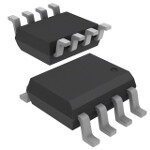
ICGOO电子元器件商城为您提供AD8091ARZ由Analog设计生产,在icgoo商城现货销售,并且可以通过原厂、代理商等渠道进行代购。 AD8091ARZ价格参考¥2.63-¥2.63。AnalogAD8091ARZ封装/规格:线性 - 放大器 - 仪表,运算放大器,缓冲器放大器, 电压反馈 放大器 1 电路 满摆幅 8-SOIC。您可以下载AD8091ARZ参考资料、Datasheet数据手册功能说明书,资料中有AD8091ARZ 详细功能的应用电路图电压和使用方法及教程。
AD8091ARZ 是 Analog Devices Inc. 生产的一款高性能、低功耗电压反馈型运算放大器,广泛应用于需要高精度和高速信号处理的场合。其主要应用场景包括:

1. 工业自动化与控制系统:用于传感器信号放大、调节和处理,如温度、压力、流量等模拟信号的调理电路。

2. 测试与测量设备:在示波器、万用表、信号发生器等仪器中作为前置放大器或缓冲器,提供高精度信号处理。

3. 通信系统:用于射频(RF)接收链中的中频(IF)信号放大,以及通信设备中的信号调理和驱动。

4. 医疗设备:如心电图仪、监护仪等,用于放大微弱生物电信号,要求高线性度和低噪声性能。

5. 音频处理设备:用于高保真音频信号的放大与处理,适合对音质要求较高的专业音频设备。

6. 汽车电子系统:如传感器接口、车载信号调理模块等,适用于对稳定性和可靠性有较高要求的环境。

AD8091ARZ具备高带宽(125 MHz)、低功耗(每个放大器仅需5.2 mA电流)和良好的失真性能,适合在多种高性能模拟电路中使用。
| 参数 | 数值 |
| -3db带宽 | 110MHz |
| 产品目录 | 集成电路 (IC)半导体 |
| 描述 | IC OPAMP VFB 110MHZ RRO 8SOIC高速运算放大器 RR SGL |
| DevelopmentKit | AD8091AR-EBZ |
| 产品分类 | Linear - Amplifiers - Instrumentation, OP Amps, Buffer Amps集成电路 - IC |
| 品牌 | Analog Devices |
| 产品手册 | |
| 产品图片 |
|
| rohs | 符合RoHS无铅 / 符合限制有害物质指令(RoHS)规范要求 |
| 产品系列 | 放大器 IC,高速运算放大器,Analog Devices AD8091ARZ- |
| 数据手册 | |
| 产品型号 | AD8091ARZ |
| 产品 | Voltage Feedback Amplifier |
| 产品培训模块 | http://www.digikey.cn/PTM/IndividualPTM.page?site=cn&lang=zhs&ptm=30008http://www.digikey.cn/PTM/IndividualPTM.page?site=cn&lang=zhs&ptm=26202 |
| 产品目录页面 | |
| 产品种类 | |
| 供应商器件封装 | 8-SOIC N |
| 共模抑制比—最小值 | 88 dB |
| 关闭 | No Shutdown |
| 包装 | 管件 |
| 压摆率 | 170 V/µs |
| 商标 | Analog Devices |
| 增益带宽生成 | 50 MHz |
| 增益带宽积 | - |
| 安装类型 | 表面贴装 |
| 安装风格 | SMD/SMT |
| 封装 | Tube |
| 封装/外壳 | 8-SOIC(0.154",3.90mm 宽) |
| 封装/箱体 | SOIC-8 |
| 工作温度 | -40°C ~ 85°C |
| 工作电源电压 | 3 V to 12 V |
| 工厂包装数量 | 98 |
| 带宽 | 110 MHz |
| 拓扑结构 | Voltage Feedback |
| 放大器类型 | 电压反馈 |
| 最大工作温度 | + 85 C |
| 最小工作温度 | - 40 C |
| 标准包装 | 98 |
| 电压-电源,单/双 (±) | 3 V ~ 12 V, ±1.5 V ~ 6 V |
| 电压-输入失调 | 1.8mV |
| 电压增益dB | 98 dB |
| 电流-电源 | 4.8mA |
| 电流-输入偏置 | 1.4µA |
| 电流-输出/通道 | 45mA |
| 电源电压-最大 | 12 V |
| 电源电压-最小 | 3 V |
| 电源电流 | 5.5 mA |
| 电路数 | 1 |
| 稳定时间 | 50 ns |
| 系列 | AD8091 |
| 视频文件 | http://www.digikey.cn/classic/video.aspx?PlayerID=1364138032001&width=640&height=505&videoID=2245193153001http://www.digikey.cn/classic/video.aspx?PlayerID=1364138032001&width=640&height=505&videoID=2245193159001 |
| 转换速度 | 145 V/us |
| 输入补偿电压 | 1.6 mV |
| 输出电流 | 45 mA |
| 输出类型 | 满摆幅 |
| 通道数量 | 1 Channel |


- 商务部:美国ITC正式对集成电路等产品启动337调查
- 曝三星4nm工艺存在良率问题 高通将骁龙8 Gen1或转产台积电
- 太阳诱电将投资9.5亿元在常州建新厂生产MLCC 预计2023年完工
- 英特尔发布欧洲新工厂建设计划 深化IDM 2.0 战略
- 台积电先进制程称霸业界 有大客户加持明年业绩稳了
- 达到5530亿美元!SIA预计今年全球半导体销售额将创下新高
- 英特尔拟将自动驾驶子公司Mobileye上市 估值或超500亿美元
- 三星加码芯片和SET,合并消费电子和移动部门,撤换高东真等 CEO
- 三星电子宣布重大人事变动 还合并消费电子和移动部门
- 海关总署:前11个月进口集成电路产品价值2.52万亿元 增长14.8%


PDF Datasheet 数据手册内容提取
Low Cost, High Speed Rail-to-Rail Amplifiers AD8091/AD8092 FEATURES CONNECTION DIAGRAMS Low cost single (AD8091) and dual (AD8092) amplifiers NC 1 AD8091 8 NC Fully specified at +3 V, +5 V, and ±5 V supplies –IN 2 7 +VS Single-supply operation +IN 3 6 VOUT HigO1h1u0 ts ppMueHte zdsw, a−inn3dg d sfBa t sobt a wsneidtthtwliinind g2th 5o (mnG 5V = Vo + f1 e)i ther rail –VS N4C = NO CONNECT5 NC 02859-001 Figure 1. SOIC-8 (R-8) 145 V/μs slew rate 50 ns settling time to 0.1% AD8091 Good video specifications (G = +2) VOUT 1 5 +VS Gain flatness of 0.1 dB to 20 MHz; RL = 150 Ω –VS 2 00..0033%%d diiffffeerreennttiiaall pghaainse e errroror;r R; RL L= = 1 1 k kΩΩ +IN 3 4 –IN 02859-003 Low distortion Figure 2. SOT23-5 (RJ-5) −80 dBc total harmonic @ 1 MHz; R = 100 Ω L Outstanding load drive capability AD8092 OUT1 1 8 +VS Drives 45 mA, 0.5 V from supply rails –IN1 2 7 OUT Drives 50 pF capacitive load (G = +1) +IN1 3 6 –IN2 Low power of 4.4 mA per amplifier –VS 4 5 +IN2 APPLICATIONS NC = NO CONNECT 02859-002 Coaxial cable drivers Figure 3. MSOP-8 and SOIC-8 (RM-8, R-8) Active filters Video switchers Professional cameras CCD imaging systems CDs/DVDs Clock buffers GENERAL DESCRIPTION The AD8091/AD8092 offer a low power supply current and can operate on a single 3 V power supply. These features are ideally The AD8091 (single) and AD8092 (dual) are low cost, voltage suited for portable and battery-powered applications where size feedback, high speed amplifiers designed to operate on +3 V, and power are critical. +5 V, or ±5 V supplies. The AD8091/AD8092 have true single- supply capability, with an input voltage range extending 200 mV The wide bandwidth and fast slew rate make these amplifiers below the negative rail and within 1 V of the positive rail. useful in many general-purpose, high speed applications where dual power supplies of up to ±6 V and single supplies from +3 Despite their low cost, the AD8091/AD8092 provide excellent V to +12 V are needed. overall performance and versatility. The output voltage swing extends to within 25 mV of each rail, providing the maximum This low cost performance is offered in an 8-lead SOIC output dynamic range with excellent overdrive recovery. This (AD8091/AD8092), a tiny SOT23-5 (AD8091), and an MSOP makes the AD8091/AD8092 useful for video electronics, such (AD8092). as cameras, video switchers, or any high speed portable equip- ment. Low distortion and fast settling make them ideal for active filter applications. Rev. C Information furnished by Analog Devices is believed to be accurate and reliable. However, no responsibility is assumed by Analog Devices for its use, nor for any infringements of patents or other One Technology Way, P.O. Box 9106, Norwood, MA 02062-9106, U.S.A. rights of third parties that may result from its use. Specifications subject to change without notice. No license is granted by implication or otherwise under any patent or patent rights of Analog Devices. Tel: 781.329.4700 www.analog.com Trademarks and registered trademarks are the property of their respective owners. Fax: 781.461.3113 ©2002–2007 Analog Devices, Inc. All rights reserved.
AD8091/AD8092 TABLE OF CONTENTS Features..............................................................................................1 Power Supply Bypassing............................................................12 Applications.......................................................................................1 Grounding...................................................................................12 Connection Diagrams......................................................................1 Input Capacitance......................................................................12 General Description.........................................................................1 Input-to-Output Coupling........................................................12 Revision History...............................................................................2 Driving Capacitive Loads..............................................................13 Specifications.....................................................................................3 Overdrive Recovery...................................................................13 Absolute Maximum Ratings............................................................6 Active Filters...............................................................................13 ESD Caution..................................................................................6 Sync Stripper...............................................................................14 Maximum Power Dissipation.....................................................7 Single-Supply Composite Video Line Driver.........................14 Typical Performance Characteristics.............................................8 Outline Dimensions.......................................................................16 Layout, Grounding, and Bypassing Considerations..................12 Ordering Guide..........................................................................17 REVISION HISTORY 9/07—Rev. B to Rev. C Changes to Applications Section....................................................1 Updated Outline Dimensions.......................................................16 Changes to Ordering Guide..........................................................17 3/05—Rev. A to Rev. B Changes to Format.............................................................Universal Changes to Features..........................................................................1 Updated Outline Dimensions.......................................................17 Changes to Ordering Guide..........................................................18 5/02–Rev. 0 to Rev. A Edits to Product Description..........................................................1 Edit to TPC 6 ....................................................................................7 Edits to TPCs 21–24.......................................................................10 Edits to Figure 3..............................................................................11 2/02—Revision 0: Initial Version Rev. C | Page 2 of 20
AD8091/AD8092 SPECIFICATIONS T = 25°C, V = 5 V, R = 2 kΩ to 2.5 V, unless otherwise noted. A S L Table 1. Parameter Conditions Min Typ Max Unit DYNAMIC PERFORMANCE −3 dB Small Signal Bandwidth G = +1, V = 0.2 V p-p 70 110 MHz O G = −1, +2, V = 0.2 V p-p 50 MHz O Bandwidth for 0.1 dB Flatness G = +2, V = 0.2 V p-p, 20 MHz O R = 150 Ω to 2.5 V, R = 806 Ω L F Slew Rate G = −1, V = 2 V step 100 145 V/μs O Full Power Response G = +1, V = 2 V p-p 35 MHz O Settling Time to 0.1% G = −1, V = 2 V step 50 ns O NOISE/DISTORTION PERFORMANCE Total Harmonic Distortion (See Figure 11) f = 5 MHz, V = 2 V p-p, G = +2 −67 dB C O Input Voltage Noise f = 10 kHz 16 nV/√Hz Input Current Noise f = 10 kHz 850 fA/√Hz Differential Gain Error (NTSC) G = +2, R = 150 Ω to 2.5 V 0.09 % L R = 1 kΩ to 2.5 V 0.03 % L Differential Phase Error (NTSC) G = +2, R = 150 Ω to 2.5 V 0.19 Degrees L R = 1 kΩ to 2.5 V 0.03 Degrees L Crosstalk f = 5 MHz, G = +2 −60 dB DC PERFORMANCE Input Offset Voltage 1.7 10 mV T to T 25 mV MIN MAX Offset Drift 10 μV/°C Input Bias Current 1.4 2.5 μA T to T 3.25 μA MIN MAX Input Offset Current 0.1 0.75 μA Open-Loop Gain R = 2 kΩ to 2.5 V 86 98 dB L T to T 96 dB MIN MAX R = 150 Ω to 2.5 V 76 82 dB L T to T 78 dB MIN MAX INPUT CHARACTERISTICS Input Resistance 290 kΩ Input Capacitance 1.4 pF Input Common-Mode Voltage Range −0.2 to +4 V Common-Mode Rejection Ratio V = 0 V to 3.5 V 72 88 dB CM OUTPUT CHARACTERISTICS Output Voltage Swing R = 10 kΩ to 2.5 V 0.015 to 4.985 V L R = 2 kΩ to 2.5 V 0.100 to 4.900 0.025 to 4.975 V L R = 150 Ω to 2.5 V 0.300 to 4.625 0.200 to 4.800 V L Output Current V = 0.5 V to 4.5 V 45 mA OUT T to T 45 mA MIN MAX Short-Circuit Current Sourcing 80 mA Sinking 130 mA Capacitive Load Drive G = +1 50 pF POWER SUPPLY Operating Range 3 12 V Quiescent Current/Amplifier 4.4 5 mA Power Supply Rejection Ratio ΔV = ±1 V 70 80 dB S OPERATING TEMPERATURE RANGE −40 +85 °C Rev. C | Page 3 of 20
AD8091/AD8092 T = 25°C, V = +3 V, R = 2 kΩ to +1.5 V, unless otherwise noted. A S L Table 2. Parameter Conditions Min Typ Max Unit DYNAMIC PERFORMANCE −3 dB Small Signal Bandwidth G = +1, V = 0.2 V p-p 70 110 MHz O G = −1, +2, V = 0.2 V p-p 50 MHz O Bandwidth for 0.1 dB Flatness G = +2, V = 0.2 V p-p, 17 MHz O R = 150 Ω to 2.5 V, R = 402 Ω L F Slew Rate G = −1, V = 2 V step 90 135 V/μs O Full Power Response G = +1, V = 1 V p-p 65 MHz O Settling Time to 0.1% G = −1, V = 2 V step 55 ns O NOISE/DISTORTION PERFORMANCE Total Harmonic Distortion (see Figure 11) f = 5 MHz, V = 2 V p-p, G = −1, −47 dB C O R = 100 Ω to 1.5 V L Input Voltage Noise f = 10 kHz 16 nV/√Hz Input Current Noise f = 10 kHz 600 fA/√Hz Differential Gain Error (NTSC) G = +2, V = 1 V CM R = 150 Ω to 1.5 V 0.11 % L R = 1 kΩ to 1.5 V 0.09 % L Differential Phase Error (NTSC) G = +2, V = 1 V CM R = 150 Ω to 1.5 V 0.24 Degrees L R = 1 kΩ to 1.5 V 0.10 Degrees L Crosstalk f = 5 MHz, G = +2 −60 dB DC PERFORMANCE Input Offset Voltage 1.6 10 mV T to T 25 mV MIN MAX Offset Drift 10 μV/°C Input Bias Current 1.3 2.6 μA T to T 3.25 μA MIN MAX Input Offset Current 0.15 0.8 μA Open-Loop Gain R = 2 kΩ 80 96 dB L T to T 94 dB MIN MAX R = 150 Ω 74 82 dB L T to T 76 dB MIN MAX INPUT CHARACTERISTICS Input Resistance 290 kΩ Input Capacitance 1.4 pF Input Common-Mode Voltage Range −0.2 to +2.0 V Common-Mode Rejection Ratio V = 0 V to 1.5 V 72 88 dB CM OUTPUT CHARACTERISTICS Output Voltage Swing R = 10 kΩ to 1.5 V 0.01 to 2.99 V L R = 2 kΩ to 1.5 V 0.075 to 2.9 0.02 to 2.98 V L R = 150 Ω to 1.5 V 0.20 to 2.75 0.125 to 2.875 V L Output Current V = 0.5 V to 2.5 V 45 mA OUT T to T 45 mA MIN MAX Short Circuit Current Sourcing 60 mA Sinking 90 mA Capacitive Load Drive G = +1 45 pF POWER SUPPLY Operating Range 3 12 V Quiescent Current/Amplifier 4.2 4.8 mA Power Supply Rejection Ratio ΔV = +0.5 V 68 80 dB S OPERATING TEMPERATURE RANGE −40 +85 °C Rev. C | Page 4 of 20
AD8091/AD8092 T = 25°C, V = ±5 V, R = 2 kΩ to ground, unless otherwise noted. A S L Table 3. Parameter Conditions Min Typ Max Unit DYNAMIC PERFORMANCE −3 dB Small Signal Bandwidth G = +1, V = 0.2 V p-p 70 110 MHz O G = −1, +2, V = 0.2 V p-p 50 MHz O Bandwidth for 0.1 dB Flatness G = +2, V = 0.2 V p-p, 20 MHz O R = 150 Ω, R = 1.1 kΩ L F Slew Rate G = −1, V = 2 V step 105 170 V/μs O Full Power Response G = +1, V = 2 V p-p 40 MHz O Settling Time to 0.1% G = −1, V = 2 V step 50 ns O NOISE/DISTORTION PERFORMANCE Total Harmonic Distortion (see Figure 11) f = 5 MHz, V = 2 V p-p, G = +2 −71 dB C O Input Voltage Noise f = 10 kHz 16 nV/√Hz Input Current Noise f = 10 kHz 900 fA/√Hz Differential Gain Error (NTSC) G = +2, R = 150 Ω 0.02 % L R = 1 kΩ 0.02 % L Differential Phase Error (NTSC) G = +2, R = 150 Ω 0.11 Degrees L R = 1 kΩ 0.02 Degrees L Crosstalk f = 5 MHz, G = +2 −60 dB DC PERFORMANCE Input Offset Voltage 1.8 11 mV T to T 27 mV MIN MAX Offset Drift 10 μV/°C Input Bias Current 1.4 2.6 μA T to T 3.5 μA MIN MAX Input Offset Current 0.1 0.75 μA Open-Loop Gain R = 2 kΩ 88 96 dB L T to T 96 dB MIN MAX R = 150 Ω 78 82 dB L T to T 80 dB MIN MAX INPUT CHARACTERISTICS Input Resistance 290 kΩ Input Capacitance 1.4 pF Input Common-Mode Voltage Range −5.2 to +4.0 V Common-Mode Rejection Ratio V = −5 V to +3.5 V 72 88 dB CM OUTPUT CHARACTERISTICS Output Voltage Swing R = 10 kΩ −4.98 to +4.98 V L R = 2 kΩ −4.85 to +4.85 −4.97 to +4.97 V L R = 150 Ω −4.45 to +4.30 −4.60 to +4.60 V L Output Current V = −4.5 V to +4.5 V 45 mA OUT T to T 45 mA MIN MAX Short Circuit Current Sourcing 100 mA Sinking 160 mA Capacitive Load Drive G = +1 (AD8091/AD8092) 50 pF POWER SUPPLY Operating Range 3 12 V Quiescent Current/Amplifier 4.8 5.5 mA Power Supply Rejection Ratio ΔV = ±1 V 68 80 dB S OPERATING TEMPERATURE RANGE −40 +85 °C Rev. C | Page 5 of 20
AD8091/AD8092 ABSOLUTE MAXIMUM RATINGS Table 4. Stresses above those listed under Absolute Maximum Ratings Parameter Rating may cause permanent damage to the device. This is a stress Supply Voltage 12.6 V rating only; functional operation of the device at these or any Power Dissipation See Figure 4 other conditions above those indicated in the operational Common-Mode Input Voltage ±VS section of this specification is not implied. Exposure to absolute Differential Input Voltage ±2.5 V maximum rating conditions for extended periods may affect Output Short-Circuit Duration See Figure 4 device reliability. Storage Temperature Range −65°C to +125°C ESD CAUTION Operating Temperature Range −40°C to +85°C Lead Temperature (Soldering 10 sec) 300°C Rev. C | Page 6 of 20
AD8091/AD8092 MAXIMUM POWER DISSIPATION The maximum safe power dissipation in the AD8091/AD8092 If the rms signal levels are indeterminate, then consider the package is limited by the associated rise in junction temperature worst case when V = V/4 for R to midsupply OUT S L (T) on the die. The plastic encapsulating the die locally reaches J ⎛V ⎞2 the junction temperature. At approximately 150°C, which is the ⎜ S ⎟ ( ) ⎝ 4 ⎠ glass transition temperature, the plastic changes its properties. P = V ×I + D S S R Even temporarily exceeding this temperature limit may change L the stresses that the package exerts on the die, permanently In single-supply operation with R referenced to −V, the worst L S shifting the parametric performance of the AD8091/AD8092. case is V = V/2. OUT S Exceeding a junction temperature of 175°C for an extended Airflow increases heat dissipation, effectively reducing θ . Also, JA period of time can result in changes in the silicon devices, more metal directly in contact with the package leads from potentially causing failure. metal traces, through holes, ground, and power planes reduces The still-air thermal properties of the package (θJA), the ambient the θJA. Care must be taken to minimize parasitic capacitances temperature (TA), and the total power dissipated in the package at the input leads of high speed op amps as discussed in the (PD) can be used to determine the junction temperature of the die. Input Capacitance section. The junction temperature can be calculated as Figure 4 shows the maximum safe power dissipation in the ( ) package vs. the ambient temperature for the SOIC-8 T =T + P ×θ J A D JA (125°C/W), SOT23-5 (180°C/W), and MSOP-8 (150°C/W) on a The power dissipated in the package (PD) is the sum of the JEDEC standard four-layer board. quiescent power dissipation and the power dissipated in the 2.0 package due to the load drive for all outputs. The quiescent TJ = 150°C power is the voltage between the supply pins (VS) times the W) quiescent current (IS). Assuming that the load (RL) is referenced ON ( 1.5 to midsupply, then the total drive power is VS/2 × IOUT, some of ATI SOIC-8 P which is dissipated in the package and some in the load SI S MSOP-8 (V × I ). The difference between the total drive power and DI OUT OUT R 1.0 E the load power is the drive power dissipated in the package. W O ( ) P PD =quiescent power+ totaldrivepower−load power UM SOT23-5 M 0.5 XI PD =(VS ×IS)+⎜⎜⎝⎛⎜⎜⎝⎛V2S ×VROULT ⎟⎟⎠⎞ −⎜⎜⎝⎛VORULT2⎟⎟⎠⎞⎟⎟⎠⎞ MA 0 02859-004 RMS output voltages should be considered. If R is referenced to –40 –30 –20 –10 0 10 20 30 40 50 60 70 80 90 L AMBIENT TEMPERATURE (°C) −V, as in single-supply operation, then the total drive power is S Figure 4. Maximum Power Dissipation vs. VS × IOUT. Temperature for a Four-Layer Board Rev. C | Page 7 of 20
AD8091/AD8092 TYPICAL PERFORMANCE CHARACTERISTICS 3 6.3 2 G = +2 6.2 RF = 2kΩ 1 6.1 dB) 0 B) 6.0 ZED GAIN ( ––21 GRF = = + 21k0Ω GRF = = + 25kΩ GRF = = + 01Ω ATNESS (d 55..89 MALI –3 N FL 5.7 R AI O –4 G 5.6 N VS = 5V VS = 5V –5 GAINAS SHOWN 5.5 G = +2 ––76 RVROFL A== S 20 k.S2ΩHVO pW-pN 02859-005 55..34 RRVOLF === 18050.206VkΩ Ωp-p 02859-008 0.1 1 10 100 500 0.1 1 10 100 FREQUENCY (MHz) FREQUENCY (MHz) Figure 5. Normalized Gain vs. Frequency; VS = +5 V Figure 8. 0.1 dB Gain Flatness vs. Frequency; G = +2 3 9 2 8 VS = +3V VS = +5V 1 7 0 6 VS = +5V AIN (dB) ––21 VS = ±5V AIN (dB) 45 VVSO == ±45VV p-p VO = 2V p-p G –3 G 3 –4 2 VSAS SHOWN –5 VSAS SHOWN 1 G = +2 ––76 VGROL = == + 201k.2ΩV p-p 02859-006 –10 RVROLF ==A S22 kkSΩΩHOWN 02859-009 0.1 1 10 100 500 0.1 1 10 100 500 FREQUENCY (MHz) FREQUENCY (MHz) Figure 6. Gain vs. Frequency vs. Supply Figure 9. Large Signal Frequency Response; G = +2 3 70 VS = 5V 2 60 RL = 2kΩ –40°C 1 50 0 B) GAIN (dB) –––321 +85°+C25°C N-LOOP GAIN (d 234000 PHASE GAIN –045 HASE (Degrees) E 10 –90 P –4 OP VS = 5V 0 –135 –5 G = +1 ––76 RVTEOL M == P 20Ek.2RΩVA TpU-pREAS SHOWN 02859-007 ––2100 5M0A° RPGHIANSE –180 02859-010 0.1 1 10 100 500 0.1 1 10 100 500 FREQUENCY (MHz) FREQUENCY (MHz) Figure 7. Gain vs. Frequency vs. Temperature Figure 10. Open-Loop Gain and Phase vs. Frequency Rev. C | Page 8 of 20
AD8091/AD8092 –20 0.10 TORTION (dBc) –––543000 VVROSL === 512V0V0, pΩG-p = +1 VRSF == 25VkΩ, G, R =L +=2 100VRΩSF == 32VkΩ, G, R =L – =1 100Ω DIFFERENTIALGAIN ERROR (%)––000000......0000004224680 NRVSTF S==C 52 ,kS ΩGU, B =RS +LC2ARSIB SEHRO (W3.5N8MHz) RRLL == 11k5Ω0Ω DIS –60 –0.060 10 20 30 40 50 60 70 80 90 100 TOTAL HARMONIC ––1–––10987100000 VRSF == 52VkΩ, G, R =L +=2 2kΩ VRSL == 52VkΩ, G = +1 02859-011 DIFFERENTIALPHASE ERROR (Degrees)–––––0000000.......011221050505050 VRSF == 52,k ΩG, =R +L2AS SHOWN RL = 1kRΩL = 150Ω 02859-014 1 2 3 4 5 6 7 8 9 10 0 10 20 30 40 50 60 70 80 90 100 FUNDAMENTAL FREQUENCY (MHz) MODULATING RAMP LEVEL (IRE) Figure 11. Total Harmonic Distortion Figure 14. Differential Gain and Phase Errors –30 1000 VS = 5V –40 10MHz –50 Bc) –60 Hz) ONIC (d –70 SE (nA 100 HARM –80 5MHz E NOI ORST –1–0900 1MHz OLTAG 10 W V –110 ––113200 GVRSL = == + 252kVΩ 02859-012 1 02859-015 0 0.5 1.0 1.5 2.0 2.5 3.0 3.5 4.0 4.5 5.0 10 100 1k 10k 100k 1M 10M OUTPUT VOLTAGE (V p-p) FREQUENCY (Hz) Figure 12. Worst Harmonic vs. Output Voltage Figure 15. Input Voltage Noise vs. Frequency 5.0 100 p) VS = 5V p- 4.5 VS = 5V V G = –1 %) ( 4.0 RF= 2kΩ D£ 0.5 3.5 RL= 2kΩ A Hz) 10 G (TH 3.0 SE (p WIN 2.5 NOI S T LTAGE 12..50 URREN 1 O C V T 1.0 U OUTP 0.05 02859-013 0.1 02859-016 0.1 1 10 50 10 100 1k 10k 100k 1M 10M FREQUENCY (MHz) FREQUENCY (Hz) Figure 13. Low Distortion Rail-to-Rail Output Swing Figure 16. Input Current Noise vs. Frequency Rev. C | Page 9 of 20
AD8091/AD8092 –10 20 VS = 5V VS = 5V –20 RF = 2kΩ 10 RL = 2kΩ –30 VO = 2V p-p 0 –10 B) –40 –PSRR SSTALK (d ––5600 SRR (dB) ––2300 +PSRR O P –40 R C –70 –50 –80 –60 –1–0900 02859-017 ––7800 02859-020 0.1 1 10 100 500 0.01 0.1 1 10 100 500 FREQUENCY (MHz) FREQUENCY (MHz) Figure 17. AD8092 Crosstalk (Output-to-Output) vs. Frequency Figure 20. PSRR vs. Frequency 0 70 VS = 5V VS = 5V –10 G = –1 60 RL = 2kΩ –20 s) –30 % (n 50 1 B) –40 O 0. 40 d T CMRR ( ––5600 G TIME 30 N LI –70 TT 20 E –80 S 10 –1–0900 02859-018 0 02859-021 0.03 0.1 1 10 100 500 0.5 1.0 1.5 2.0 FREQUENCY (MHz) INPUT STEPS (V p-p) Figure 18. CMRR vs. Frequency Figure 21. Settling Time vs. Input Step 100.000 1.0 VGS = = + 51V 0.9 VS = 5V VOH = +85°C 31.000 V) E ( 0.8 VOH = +25°C STANCE (Ω)103..010000 ON VOLTAG 00..76 VOH = –40°C VOL = +85°C RESI 1.000 RATI 0.5 UT 0.310 ATU 0.4 P S OUT 0.100 PUT 0.3 VOL = +25°C OUT 0.2 VOL = –40°C 00..003110 02859-019 0.10 02859-022 0.1 1 10 100 500 0 5 10 15 20 25 30 35 40 45 50 55 60 65 70 75 80 85 FREQUENCY (MHz) LOAD CURRENT (mA) Figure 19. Closed-Loop Output Resistance vs. Frequency Figure 22. Output Saturation Voltage vs. Load Current Rev. C | Page 10 of 20
AD8091/AD8092 100 RL = 2kΩ VGS = = + 52V RL = 2kΩ 90 VIN = 1V p-p B) 3.5V d N ( AI RL = 150Ω G P 80 2.5V O O L N- E 1.5V P O 70 60 VS = 5V 02859-023 02859-026 0 0.5 1.0 1.5 2.0 2.5 3.0 3.5 4.0 4.5 5.0 OUTPUT VOLTAGE (V) Figure 23. Open-Loop Gain vs. Output Voltage Figure 26. Large Signal Step Response; VS = +5 V, G = +2 VIN = 0.1V p-p VS = 5V G = +1 G = –1 RL = 2kΩ RF = 2kΩ VS = 3V RL = 2kΩ 5V 1.50V 2.5V 20mV 20ns 02859-024 1V 2µs 02859-027 Figure 24. 100 mV Step Response; G = +1 Figure 27. Output Swing; G = −1, RL = 2 kΩ GVS = = + 51V 4V VGS = = + ±15V RL = 2kΩ 3V RL = 2kΩ 2.60V 2V 1V 2.50V –1V 2.40V –2V –3V –4V 50mV 20ns 02859-025 1V 20ns 02859-028 Figure 25. 200 mV Step Response; VS = +5 V, G = +1 Figure 28. Large Signal Step Response; VS = ±5 V, G = +1 Rev. C | Page 11 of 20
AD8091/AD8092 LAYOUT, GROUNDING, AND BYPASSING CONSIDERATIONS POWER SUPPLY BYPASSING The lengths of the high frequency bypass capacitor leads are most critical. A parasitic inductance in the bypass grounding Power supply pins are actually inputs, and care must be taken so works against the low impedance created by the bypass that a noise-free stable dc voltage is applied. The purpose of capacitor. Place the ground leads of the bypass capacitors at the bypass capacitors is to create low impedances from the supply same physical location. Because load currents flow from the to ground at all frequencies, thereby shunting or filtering a supplies as well, the ground for the load impedance should be at majority of the noise. the same physical location as the bypass capacitor grounds. For Decoupling schemes are designed to minimize the bypassing the larger value capacitors, which are intended to be effective at impedance at all frequencies with a parallel combination of lower frequencies, the current return path distance is less capacitors. Chip capacitors of 0.01 μF or 0.001 μF (X7R or critical. NPO) are critical and should be as close as possible to the INPUT CAPACITANCE amplifier package. Larger chip capacitors, such as the 0.1 μF capacitor, can be shared among a few closely spaced active Along with bypassing and ground, high speed amplifiers can components in the same signal path. A 10 μF tantalum be sensitive to parasitic capacitance between the inputs and capacitor is less critical for high frequency bypassing and, in ground. A few pF of capacitance reduces the input impedance most cases, only one per board is needed at the supply inputs. at high frequencies, in turn increasing the amplifier’s gain and causing peaking of the frequency response or even oscillations, GROUNDING if severe enough. It is recommended that the external passive A ground plane layer is important in densely packed PC boards components, which are connected to the input pins, be placed to spread the current-minimizing parasitic inductances. as close as possible to the inputs to avoid parasitic capacitance. However, an understanding of where the current flows in a The ground and power planes must be kept at a distance of at circuit is critical to implementing effective high speed circuit least 0.05 mm from the input pins on all layers of the board. design. The length of the current path is directly proportional to INPUT-TO-OUTPUT COUPLING the magnitude of parasitic inductances and thus the high The input and output signal traces should not be parallel to frequency impedance of the path. High speed currents in an inductive ground return create an unwanted voltage noise. minimize capacitive coupling between the inputs and output and to avoid any positive feedback. Rev. C | Page 12 of 20
AD8091/AD8092 DRIVING CAPACITIVE LOADS A highly capacitive load reacts with the output of the amplifiers, 10000 VS = 5V causing a loss in phase margin and subsequent peaking or even £30% OVERSHOOT oscillation, as shown in Figure 29 and Figure 30. There are two RS = 3Ω methods to effectively minimize its effect. F)1000 p • Put a small value resistor in series with the output to isolate D ( A O the load capacitor from the amplifier’s output stage. E L 100 RS = 0Ω • Increase the phase margin with higher noise gains or by TIV CI adding a pole with a parallel resistor and capacitor from PA RG RF A −IN to the output. C 10 1V0IN0mV STEP RS VOUT 8 6 1 50Ω CL 02859-031 4 1 2 3 4 5 6 2 ACL (V/V) Figure 31. Capacitive Load Drive vs. Closed-Loop Gain B) 0 N (d –2 OVERDRIVE RECOVERY AI G –4 Overdrive of an amplifier occurs when the output range and/or input range is exceeded. The amplifier must recover from this –6 VS = 5V overdrive condition. The AD8091/AD8092 recover within 60 ns –8 G = +1 RL= 2kΩ from negative overdrive and within 45 ns from positive ––1120 CVOL== 5200p0FmV p-p 02859-029 overdrive, as shown in Figure 32. 0.1 1 10 100 500 FREQUENCY (MHz) VGS = = + ±55V Figure 29. Closed-Loop Frequency Response: CL = 50 pF INPUT 1V/DIV RRFL == 22kkΩΩ VS = 5V OUTPUT 2V/DIV G = +1 RL = 2kΩ CL = 50pF 2.60V 2.55V 2.50V 2.45V 2.40V V/DIVAS SHOWN 100ns 02859-032 Figure 32. Overdrive Recovery 50mV 100ns 02859-030 AAcCtiTvIeV fiElt eFrIsL aTt EhiRgShe r frequencies require wider bandwidth op Figure 30. 200 mV Step Response: CL = 50 pF amps to work effectively. Excessive phase shift produced by As the closed-loop gain is increased, the larger phase margin lower frequency op amps can significantly impact active filter allows for large capacitor loads with less peaking. Adding a low performance. value resistor in series with the load at lower gains has the same Figure 33 shows an example of a 2 MHz biquad bandwidth filter effect. Figure 31 shows the effect of a series resistor for various that uses three op amps. Such circuits are sometimes used in voltage gains. For large capacitive loads, the frequency response medical ultrasound systems to lower the noise bandwidth of the of the amplifier is dominated by the series resistor and capaci- analog signal before A/D conversion. Note that the unused tive load. amplifiers’ inputs should be tied to ground. Rev. C | Page 13 of 20
AD8091/AD8092 VIDEO WITH SYNC VIDEO WITHOUT SYNC C1 R6 50pF 1kΩ R2 2kΩ 2Rk4Ω C2 3Rk1Ω 2 R3 50pF VBLANK +0.4V GROUND VIN 1 2kΩ 6 R5 3 7 2kΩ 2 GROUND 3V OR 5V 5 6 AD8092 AD8092 3 AD8091 VOUT 02859-033 VIN 3 7 0.1µF +10µF Figure 33. 2 MHz Biquad Band-Pass Filter TOA/D AD8091 6 The frequency response of the circuit is shown in Figure 34. 2 4 100Ω R2 0 1kΩ R1 1kΩ –10 (OR 2+ ×0 .V8BVLANK) 02859-035 Figure 35. Sync Stripper dB) –20 N ( SINGLE-SUPPLY COMPOSITE VIDEO LINE DRIVER AI G Many composite video signals have their blanking level at –30 ground and have video information that is both positive and negative. Such signals require dual-supply amplifiers to pass them. However, by ac level-shifting, a single-supply amplifier –40 02859-034 can be used to pass these signals. The following complications 10k 100k 1M 10M 100M may arise from such techniques. FREQUENCY (Hz) Signals of bounded peak-to-peak amplitude that vary in duty Figure 34. Frequency Response of 2 MHz Band-Pass Biquad Filter cycle require larger dynamic swing capacity than their SYNC STRIPPER (bounded) peak-to-peak amplitude after they are ac-coupled. As a worst case, the dynamic signal swing approaches twice the Synchronizing pulses are sometimes carried on video signals so peak-to-peak value. One of two conditions that define the as not to require a separate channel to carry the synchronizing maximum dynamic swing requirements is a signal that is information. However, for some functions, such as A/D mostly low but goes high with a duty cycle that is a small conversion, it is not desirable to have the sync pulses on the fraction of a percent. The opposite condition defines the second video signal. These pulses reduce the dynamic range of the condition. video signal and do not provide any useful information for such a function. The worst case of composite video is not quite this demanding. One bounding condition is a signal that is mostly black for an A sync stripper removes the synchronizing pulses from a video entire frame but has a white (full amplitude) minimum width signal while passing all the useful video information. Figure 35 spike at least once in a frame. shows a practical single-supply circuit that uses only a single AD8091. It is capable of directly driving a reverse terminated The other extreme is a full white video signal. The blanking video line. intervals and sync tips of such a signal have negative-going excursions in compliance with the composite video The video signal plus sync is applied to the noninverting input specifications. The combination of horizontal and vertical with the proper termination. The amplifier gain is set equal to 2 blanking intervals limit such a signal to being at the highest via the two 1 kΩ resistors in the feedback circuit. A bias voltage (white) level for a maximum of about 75% of the time. must be applied to R1 for the input signal to have the sync pulses stripped at the proper level. As a result of the duty cycles between the two extremes, a 1 V p-p composite video signal that is multiplied by a gain of 2 The blanking level of the input video pulse is the desired place requires about 3.2 V p-p of dynamic voltage swing at the output to remove the sync information. The amplifier multiplies this for an op amp to pass a composite video signal of arbitrary level by 2. This level must be at ground at the output in order varying duty cycle without distortion. for the sync stripping action to take place. Because the gain of the amplifier from the input of R1 to the output is −1, a voltage equal to 2 × V must be applied to make the blanking level BLANK come out at ground. Rev. C | Page 14 of 20
AD8091/AD8092 Some circuits use a sync tip clamp to hold the sync tips at a The feedback circuit provides unity gain for the dc biasing of relatively constant level to lower the amount of dynamic signal the input and provides a gain of 2 for any signals that are in the swing required. However, these circuits can have artifacts like video bandwidth. The output is ac-coupled and terminated to sync tip compression unless they are driven by a source with a drive the line. very low output impedance. The AD8091/AD8092 have The capacitor values provide minimum tilt or field time adequate signal swing when running on a single 5 V supply to distortion of the video signal. These values are required for handle an ac-coupled composite video signal. video that is considered to be studio or broadcast quality. The input to the circuit shown in Figure 36 is a standard However, if a lower consumer grade of video, sometimes composite (1 V p-p) video signal that has the blanking level at referred to as consumer video, is all that is desired, the values ground. The input network level shifts the video signal by and the cost of the capacitors can be reduced by as much as a means of ac coupling. The noninverting input of the op amp is factor of 5 with minimum visible degradation in the picture. biased to half of the supply voltage. 5V 4.99kΩ + 4.99kΩ 10µF + 0.1µF 10µF 47µF COMVIPDOESOI TINE 75RΩT + 10kΩ 3AD80791 6 10+00µF 7R5BΩT RL VOUT 2 4 75Ω RF 0.1µF 1kΩ RG 1kΩ 220µF 02859-036 Figure 36. Single-Supply Composite Video Line Driver Rev. C | Page 15 of 20
AD8091/AD8092 OUTLINE DIMENSIONS 5.00(0.1968) 3.20 4.80(0.1890) 3.00 2.80 8 5 4.00 (0.1574) 6.20 (0.2441) 3.80 (0.1497) 1 4 5.80 (0.2284) 3.20 8 5 54..1950 3.00 4.65 2.80 1 4 1.27 (0.0500) 0.50 (0.0196) BSC 1.75 (0.0688) 0.25 (0.0099) 45° PIN 1 0.25 (0.0098) 1.35 (0.0532) 8° 0.65 BSC 0.10 (0.0040) 0° 0.95 COPL0A.1N0ARITSYEATING 00..5311 ((00..00210212)) 0.25 (0.0098) 10..2470 ((00..00510507)) 00..8755 1.10 MAX PLANE 0.17 (0.0067) 0.80 0.15 0.38 0.23 8° 0.60 COMPLIANTTO JEDEC STANDARDS MS-012-AA 0.00 0.22 0.08 0° 0.40 C(RINOEFNPEATRRREOENNLCLTEIHN EOGSN EDLSIYM)AEANNRDSEI AORRNOESU NANORDEET DAIN-PO MPFRIFLO LMPIIMRLELIATIMTEEER TFSEO; RIRN ECUQHSU EDI VIINMA LEDENENSSTIIOGSN NFS.OR 012407-A COPL0A.1N0ARITY SPELAANTIENG Figure 37. 8-Lead Standard Small Outline Package [SOIC_N] COMPLIANT TO JEDEC STANDARDS MO-187-AA Narrow Body (R-8) Figure 38. 8-Lead Mini Small Outline Package [MSOP] Dimensions shown in millimeters and (inches) (RM-8) Dimensions shown in millimeters 2.90 BSC 5 4 1.60 BSC 2.80 BSC 1 2 3 PIN 1 0.95 BSC 1.30 B1.S9C0 1.15 0.90 1.45 MAX 0.22 0.08 10° 0.15 MAX 0.50 SEATING 5° 0.60 0.30 PLANE 0° 0.45 0.30 COMPLIANTTO JEDEC STANDARDS MO-178-AA Figure 39. 5-Lead Small Outline Transistor Package [SOT-23] (RJ-5) Dimensions shown in millimeters Rev. C | Page 16 of 20
AD8091/AD8092 ORDERING GUIDE Model Temperature Range Package Description Package Option Branding AD8091AR −40°C to +85°C 8-Lead SOIC R-8 AD8091AR-REEL −40°C to +85°C 8-Lead SOIC, 13” Tape and Reel R-8 AD8091AR-REEL7 −40°C to +85°C 8-Lead SOIC, 7” Tape and Reel R-8 AD8091ARZ1 −40°C to +85°C 8-Lead SOIC R-8 AD8091ARZ-REEL1 −40°C to +85°C 8-Lead SOIC, 13” Tape and Reel R-8 AD8091ARZ-REEL71 −40°C to +85°C 8-Lead SOIC, 7” Tape and Reel R-8 AD8091ART-R2 −40°C to +85°C 5-Lead SOT-23 RJ-5 HVA AD8091ART-REEL −40°C to +85°C 5-Lead SOT-23, 13” Tape and Reel RJ-5 HVA AD8091ART-REEL7 −40°C to +85°C 5-Lead SOT-23, 7” Tape and Reel RJ-5 HVA AD8091ARTZ-R21 −40°C to +85°C 5-Lead SOT-23 RJ-5 HVA# AD8091ARTZ-R71 −40°C to +85°C 5-Lead SOT-23, 7” Tape and Reel RJ-5 HVA# AD8091ARTZ-RL1 −40°C to +85°C 5-Lead SOT-23, 13” Tape and Reel RJ-5 HVA# AD8092AR −40°C to +85°C 8-Lead SOIC R-8 AD8092AR-REEL −40°C to +85°C 8-Lead SOIC, 13” Tape and Reel R-8 AD8092AR-REEL7 −40°C to +85°C 8-Lead SOIC, 7” Tape and Reel R-8 AD8092ARZ1 −40°C to +85°C 8-Lead SOIC R-8 AD8092ARZ-REEL1 −40°C to +85°C 8-Lead SOIC, 13” Tape and Reel R-8 AD8092ARZ-REEL71 −40°C to +85°C 8-Lead SOIC, 7” Tape and Reel R-8 AD8092ARM −40°C to +85°C 8-Lead MSOP RM-8 HWA AD8092ARM-REEL −40°C to +85°C 8-Lead MSOP, 13" Tape and Reel RM-8 HWA AD8092ARM-REEL7 −40°C to +85°C 8-Lead MSOP, 7" Tape and Reel RM-8 HWA AD8092ARMZ1 −40°C to +85°C 8-Lead MSOP RM-8 HWA# AD8092ARMZ-REEL1 −40°C to +85°C 8-Lead MSOP, 13" Tape and Reel RM-8 HWA# AD8092ARMZ-REEL71 −40°C to +85°C 8-Lead MSOP, 7" Tape and Reel RM-8 HWA# 1 Z = RoHS Compliant Part. # denotes lead-free, may be top or bottom marked. Rev. C | Page 17 of 20
AD8091/AD8092 NOTES Rev. C | Page 18 of 20
AD8091/AD8092 NOTES Rev. C | Page 19 of 20
AD8091/AD8092 NOTES ©2002–2007 Analog Devices, Inc. All rights reserved. Trademarks and registered trademarks are the property of their respective owners. D02859-0-9/07(C) Rev. C | Page 20 of 20