ICGOO在线商城 > 集成电路(IC) > 线性 - 放大器 - 仪表,运算放大器,缓冲器放大器 > AD8055ARZ
 Datasheet下载
- 型号: AD8055ARZ
- 制造商: Analog
- 库位|库存: xxxx|xxxx
- 要求:
| 数量阶梯 | 香港交货 | 国内含税 |
| +xxxx | $xxxx | ¥xxxx |
查看当月历史价格
查看今年历史价格
AD8055ARZ产品简介:
ICGOO电子元器件商城为您提供AD8055ARZ由Analog设计生产,在icgoo商城现货销售,并且可以通过原厂、代理商等渠道进行代购。 AD8055ARZ价格参考¥7.07-¥7.33。AnalogAD8055ARZ封装/规格:线性 - 放大器 - 仪表,运算放大器,缓冲器放大器, 电压反馈 放大器 1 电路 8-SOIC。您可以下载AD8055ARZ参考资料、Datasheet数据手册功能说明书,资料中有AD8055ARZ 详细功能的应用电路图电压和使用方法及教程。
AD8055ARZ 是由 Analog Devices Inc. 生产的一款高性能运算放大器,属于线性 - 放大器 - 仪表、运算放大器、缓冲器放大器类别。它具有低噪声、高带宽和快速建立时间等特性,适用于多种精密和高速信号处理场景。以下是 AD8055ARZ 的一些典型应用场景:

1. 医疗设备
   - 在医疗电子领域,AD8055ARZ 可用于心电图(ECG)、超声波和患者监护仪等设备中。其低噪声性能确保能够准确捕捉微弱的生物电信号,同时快速响应能力支持实时监测。

2. 工业自动化与控制
   - 该放大器可用于数据采集系统、传感器接口和过程控制系统。例如,在温度、压力或位移传感器信号调理电路中,AD8055ARZ 能够提供高精度放大和稳定的输出信号。

3. 通信设备
   - AD8055ARZ 的宽带宽和低失真特性使其非常适合无线通信中的中频信号处理。它可以作为驱动器放大器,用于提高射频前端模块的性能。

4. 音频处理
   - 在专业音频设备中,如调音台、麦克风前置放大器和音频滤波器,AD8055ARZ 提供了卓越的动态范围和低失真,保证高质量的声音再现。

5. 测试与测量仪器
   - 此放大器广泛应用于示波器、频谱分析仪和其他精密测试设备中。其快速建立时间和高精度特性有助于实现更准确的测量结果。

6. 消费电子产品
   - 在某些高端消费类电子产品中,如数字相机、摄像机和家用音响系统,AD8055ARZ 能够优化图像处理和音频性能。

总之,AD8055ARZ 凭借其出色的电气特性,成为需要高精度、快速响应和低噪声解决方案的理想选择。它的多功能性和可靠性使得它在众多行业和技术领域中都有广泛应用。
| 参数 | 数值 |
| -3db带宽 | 300MHz |
| 产品目录 | 集成电路 (IC)半导体 |
| 描述 | IC OPAMP VFB 300MHZ 8SOIC高速运算放大器 SGL 300MHz VTG Feedback |
| DevelopmentKit | AD8055AR-EBZ |
| 产品分类 | Linear - Amplifiers - Instrumentation, OP Amps, Buffer Amps集成电路 - IC |
| 品牌 | Analog Devices |
| 产品手册 | |
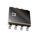
| 产品图片 |
|
| rohs | 符合RoHS无铅 / 符合限制有害物质指令(RoHS)规范要求 |
| 产品系列 | 放大器 IC,高速运算放大器,Analog Devices AD8055ARZ- |
| 数据手册 | |
| 产品型号 | AD8055ARZ |
| 产品 | Voltage Feedback Amplifier |
| 产品培训模块 | http://www.digikey.cn/PTM/IndividualPTM.page?site=cn&lang=zhs&ptm=30008http://www.digikey.cn/PTM/IndividualPTM.page?site=cn&lang=zhs&ptm=26202 |
| 产品目录页面 | |
| 产品种类 | 高速运算放大器 |
| 供应商器件封装 | 8-SOIC |
| 共模抑制比—最小值 | 82 dB |
| 关闭 | No Shutdown |
| 包装 | 管件 |
| 压摆率 | 1400 V/µs |
| 商标 | Analog Devices |
| 增益带宽生成 | 120 MHz |
| 增益带宽积 | - |
| 安装类型 | 表面贴装 |
| 安装风格 | SMD/SMT |
| 封装 | Tube |
| 封装/外壳 | 8-SOIC(0.154",3.90mm 宽) |
| 封装/箱体 | SOIC-8 |
| 工作温度 | -40°C ~ 125°C |
| 工作电源电压 | 8 V to 12 V |
| 工厂包装数量 | 98 |
| 带宽 | 300 MHz |
| 拓扑结构 | Voltage Feedback |
| 放大器类型 | 电压反馈 |
| 最大工作温度 | + 85 C |
| 最小工作温度 | - 40 C |
| 标准包装 | 98 |
| 电压-电源,单/双 (±) | 8 V ~ 12 V, ±4 V ~ 6 V |
| 电压-输入失调 | 3mV |
| 电压增益dB | 71 dB |
| 电流-电源 | 5.4mA |
| 电流-输入偏置 | 400nA |
| 电流-输出/通道 | 60mA |
| 电源电压-最大 | 12 V |
| 电源电压-最小 | 8 V |
| 电源电流 | 6.5 mA |
| 电路数 | 1 |
| 稳定时间 | 20 ns |
| 系列 | AD8055 |
| 视频文件 | http://www.digikey.cn/classic/video.aspx?PlayerID=1364138032001&width=640&height=505&videoID=2245193153001http://www.digikey.cn/classic/video.aspx?PlayerID=1364138032001&width=640&height=505&videoID=2245193159001 |
| 转换速度 | 1400 V/us |
| 输入补偿电压 | 3 mV |
| 输出电流 | 60 mA |
| 输出类型 | - |
| 通道数量 | 1 Channel |


PDF Datasheet 数据手册内容提取
Low Cost, 300 MHz Voltage Feedback Amplifiers AD8055/AD8056 FEATURES CONNECTION DIAGRAMS Low cost single (AD8055) and dual (AD8056) NC 1 8 NC Easy-to-use voltage feedback architecture VOUT 1 5 +VS High speed –IN 2 7 +VS –VS 2 300 MHz, −3 dB bandwidth (G = +1) +IN 3 6 VOUT 12400 n0s Vse/μttsl isnlegw to r a0t.e1 % –VS 4 NC=ANDO8C0O5N5NECT 5 NC 01063-001 +IN 3 AD8055 4 –IN 01063-002 Low distortion: −72 dBc @ 10 MHz Figure 1. N-8 and R-8 Figure 2. RJ-5 Low noise: 6 nV/√Hz Low dc errors: 5 mV max VOS, 1.2 μA max IB OUT1 1 8 +VS Small packaging –IN1 2 7 OUT AD8055 available in 5-lead SOT-23 +IN1 3 6 –IN2 ExcAeDll8e0n5t 6v iadveaoil sapbelec iifnic 8a-tlieoands M(RSL O=P 1 50 Ω, G = +2) –VS 4 AD8056 5 +IN2 01063-003 Figure 3. N-8, R-8, and RM-8 Gain flatness 0.1 dB to 40 MHz 0.01% differential gain error Their 0.1 dB flatness out to 40 MHz, wide bandwidth out to 0.02° differential phase error 300 MHz, along with 1400 V/μs slew rate and 20 ns settling Drives 4 video loads (37.5 V) with 0.02% differential time, make them useful for a variety of high speed applications. Gain and 0.1° differential phase Low power, ±5 V supplies 5 mA typ/amplifier power The AD8055 and AD8056 require only 5 mA typ/amplifier of supply current supply current and operate on a dual ±5 V or a single +12 V High output drive current: over 60 mA power supply, while capable of delivering over 60 mA of load current. The AD8055 is available in a small 8-lead PDIP, an 8-lead APPLICATIONS SOIC, and a 5-lead SOT-23, while the AD8056 is available in an 8-lead MSOP. These features make the AD8055/AD8056 ideal Imaging for portable and battery-powered applications where size and Photodiode preamps power are critical. These amplifiers in the R-8, N-8, and RM-8 Video line drivers packages are available in the extended temperature range of Differential line drivers −40°C to +125°C. Professional cameras Video switchers 5 Special effects 4 VIN RC VOUT VROLU=T1=001Ω00mVp-p A-to-D drivers 3 50Ω Active filters G=+1 2 RG RF RL RRFC==01Ω00Ω GENERAL DESCRIPTION dB) 1 GRF==+4202Ω N ( 0 AI The AD8055 (single) and AD8056 (dual) voltage feedback G –1 amplifiers offer bandwidth and slew rate typically found in –2 G=+10 current feedback amplifiers. Additionally, these amplifiers are –3 RF=909Ω easy to use and available at a very low cost. G=+5 –4 RF=1000Ω Dexecsepllieten tt hoevierr laolwl p ceorsfot,r tmhea nAcDe. 8F0o5r5 v aidnedo A aDpp8l0ic5a6t ipornosv,i tdhee ir –05.3M 1M FR1E0QMUENCY(Hz) 100M 1G 01063-004 differential gain and phase error are 0.01% and 0.02° into a Figure 4. Frequency Response 150 Ω load and 0.02% and 0.1° while driving four video loads (37.50 Ω). Rev. J Information furnished by Analog Devices is believed to be accurate and reliable. However, no responsibility is assumed by Analog Devices for its use, nor for any infringements of patents or other One Technology Way, P.O. Box 9106, Norwood, MA 02062-9106, U.S.A. rights of third parties that may result from its use. Specifications subject to change without notice. No license is granted by implication or otherwise under any patent or patent rights of Analog Devices. Tel: 781.329.4700 www.analog.com Trademarks and registered trademarks are the property of their respective owners. Fax: 781.461.3113 ©2006 Analog Devices, Inc. All rights reserved.
AD8055/AD8056 TABLE OF CONTENTS Features..............................................................................................1 Applications.....................................................................................12 Applications.......................................................................................1 Four-Line Video Driver.............................................................12 General Description.........................................................................1 Single-Ended-to-Differential Line Driver...............................12 Connection Diagrams......................................................................1 Low Noise, Low Power Preamp................................................12 Revision History...............................................................................2 Power Dissipation Limits..........................................................13 Specifications.....................................................................................3 Resistor Selection.......................................................................13 Absolute Maximum Ratings............................................................5 Driving Capacitive Loads..........................................................13 Maximum Power Dissipation.....................................................5 Outline Dimensions.......................................................................14 ESD Caution..................................................................................5 Ordering Guide..........................................................................16 Typical Performance Characteristics.............................................6 Test Circuits.....................................................................................11 REVISION HISTORY 2/06—Rev. I to Rev. J 10/02—Rev. E to Rev. F Changes to Format.............................................................Universal Text Changes to Reflect Extended Temperature Range for Updated Outline Dimensions.......................................................15 R-8, N-8 Packages..............................................................................1 Changes to Ordering Guide..........................................................16 Changes to Specifications.................................................................2 Changes to Absolute Maximum Ratings........................................3 Figure 2 Replaced..............................................................................3 2/04—Rev. H to Rev. I Changes to Ordering Guide.............................................................3 Changes to Features..........................................................................1 Outline Dimensions Updated.......................................................11 Changes to Ordering Guide............................................................3 7/01—Rev. D to Rev. E 6/03—Rev. G to Rev. H TPC 24 Replaced with New Graph.................................................7 Changes to Absolute Maximum Ratings.......................................3 Updated Ordering Guide.................................................................3 3/01—Rev. C to Rev. D Updated Outline Dimensions.......................................................11 Edit to Curve in TPC 23...................................................................7 2/03—Rev. F to Rev. G 2/01—Rev. B to Rev. C Changes to Product Description....................................................1 Edits to Text at Top of Specifications Page (65 to 5)....................2 Changes to Specifications................................................................2 Change to Ordering Guide..............................................................3 Outline Dimensions Updated.......................................................11 Rev. J | Page 2 of 16
AD8055/AD8056 SPECIFICATIONS T = 25°C, V = ±5 V, R = 402 Ω, R = 100 Ω, Gain = +2, unless otherwise noted. A S F L Table 1. AD8055A/AD8056A Parameter Conditions Min Typ Max Unit DYNAMIC PERFORMANCE −3 dB Bandwidth G = +1, V = 0.1 V p-p 220 300 MHz O G=+1, V = 2 V p-p 125 150 MHz O G=+2, V = 0.1 V p-p 120 160 MHz O G=+2, V = 2 V p-p 125 150 MHz O Bandwidth for 0.1 dB Flatness V = 100 mV p-p 25 40 MHz O Slew Rate G = +1, V = 4 V step 1000 1400 V/μs O G = +2, V = 4 V step 750 840 V/μs O Settling Time to 0.1% G = +2, V = 2 V step 20 ns O Rise and Fall Time, 10% to 90% G = +1, V = 0.5 V step 2 ns O G = +1, V = 4 V step 2.7 ns O G = +2, V = 0.5 V step 2.8 ns O G = +2, V = 4 V step 4 ns O NOISE/HARMONIC PERFORMANCE Total Harmonic Distortion f = 10 MHz, V = 2 V p-p, R = 1 kΩ −72 dBc C O L f = 20 MHz, V = 2 V p-p, R = 1 kΩ −57 dBc C O L Crosstalk, Output-to-Output (AD8056) f = 5 MHz, G = +2 −60 dB Input Voltage Noise f = 100 kHz 6 nV/√Hz Input Current Noise f = 100 kHz 1 pA/√Hz Differential Gain Error NTSC, G = +2, R = 150 Ω 0.01 % L NTSC, G = +2, R = 37.5 Ω 0.02 % L Differential Phase Error NTSC, G = +2, R = 150 Ω 0.02 Degree L NTSC, G = +2, R = 37.5 Ω 0.1 Degree L DC PERFORMANCE Input Offset Voltage 3 5 mV T to T 10 mV MIN MAX Offset Drift 6 μV/°C Input Bias Current 0.4 1.2 μA T to T 1 μA MIN MAX Open-Loop Gain V = ±2.5 V 66 71 dB O T to T 64 dB MIN MAX INPUT CHARACTERISTICS Input Resistance 10 MΩ Input Capacitance 2 pF Input Common-Mode Voltage Range 3.2 ±V Common-Mode Rejection Ratio V = ±2.5 V 82 dB CM OUTPUT CHARACTERISTICS Output Voltage Swing R = 150 Ω 2.9 3.1 ±V L Output Current1 V = ±2.0 V 55 60 mA O Short-Circuit Current1 110 mA Rev. J | Page 3 of 16
AD8055/AD8056 AD8055A/AD8056A Parameter Conditions Min Typ Max Unit POWER SUPPLY Operating Range ±4.0 ±5.0 ±6.0 V Quiescent Current AD8055 5.4 6.5 mA T to 125°C 7.6 mA MIN T to 85°C 7.3 mA MIN AD8056 10 12 mA T to 125°C 13.9 mA MIN T to 85°C 13.3 mA MIN Power Supply Rejection Ratio +V = +5 V to +6 V, −V = −5 V 66 72 dB S S −V = –5 V to −6 V, +V = +5 V 69 86 dB S S OPERATING TEMPERATURE RANGE AD8055ART −40 +85 °C AD8055AR, AD8055AN, AD8056AR, AD8056AN, AD8056ARM −40 +125 °C 1 Output current is limited by the maximum power dissipation in the package. See Figure 5. Rev. J | Page 4 of 16
AD8055/AD8056 ABSOLUTE MAXIMUM RATINGS Table 2. MAXIMUM POWER DISSIPATION Parameter Ratings The maximum power that can be safely dissipated by the Supply Voltage 13.2 V AD8055/AD8056 is limited by the associated rise in junction Input Voltage (Common Mode) ±V S temperature. The maximum safe junction temperature for Differential Input Voltage ±2.5 V plastic encapsulated devices is determined by the glass Output Short-Circuit Duration Observe Power transition temperature of the plastic, approximately 150°C. Derating Curves Exceeding this limit temporarily can cause a shift in parametric Storage Temperature Range N, R −65°C to +150°C performance due to a change in the stresses exerted on the die Operating Temperature Range (A Grade) −40°C to +125°C by the package. Exceeding a junction temperature of 175°C for Lead Temperature (Soldering 10 sec) 300°C an extended period can result in device failure. Stresses above those listed under Absolute Maximum Ratings may cause permanent damage to the device. This is a stress While the AD8055/AD8056 are internally short-circuit rating only; functional operation of the device at these or any protected, this may not be sufficient to guarantee that the other conditions above those indicated in the operational maximum junction temperature (150°C) is not exceeded under section of this specification is not implied. Exposure to absolute all conditions. To ensure proper operation, it is necessary to maximum rating conditions for extended periods may affect observe the maximum power derating curves. device reliability. 2.5 W) N ( 2.0 O PDIP-8 TI SOIC-8 A P SI 1.5 S DI R E W O 1.0 P M U MSOP-8 M MAXI 0.5 SOT-23-5 0–55–45–35–25–15A–5MB5IEN1T5T2E5M3P5ER45AT5U5RE65(°C75) 85 95 105115125 01063-005 Figure 5. Plot of Maximum Power Dissipation vs. Temperature for AD8055/AD8056 ESD CAUTION ESD (electrostatic discharge) sensitive device. Electrostatic charges as high as 4000 V readily accumulate on the human body and test equipment and can discharge without detection. Although this product features proprietary ESD protection circuitry, permanent damage may occur on devices subjected to high energy electrostatic discharges. Therefore, proper ESD precautions are recommended to avoid performance degradation or loss of functionality. Rev. J | Page 5 of 16
AD8055/AD8056 TYPICAL PERFORMANCE CHARACTERISTICS 0V 0V 20mV 5ns 01063-007 1V 5ns 01063-011 Figure 6. Small Step Response, G = +1 (See Figure 34) Figure 9. Large Step Response, G = −1 (See Figure 35) 5 4 VIN RC VOUT VROLU=T1=001Ω00mVp-p 3 50Ω G=+1 2 RG RF RL RRFC==01Ω00Ω dB) 1 GRF==+4202Ω 0V N ( 0 AI G –1 –2 G=+10 –3 RF=909Ω 1V 5ns 01063-008 ––054.3M 1M GRF=F=R+115E00Q0M0UΩENCY(Hz) 100M 1G 01063-012 Figure 7. Large Step Response, G = +1 (See Figure 34) Figure 10. Small Signal Frequency Response, G = +1, G = +2, G = +5, G = +10 5 VOUT=2Vp-p 4 RL=100Ω 3 2 dB) 1 GRF==+01Ω 0V N ( 0 AI G=+2 G –1 RF=402Ω –2 G=+10 –3 RF=909Ω 20mV 5ns 01063-010 ––054.3M 1M GRF=F=R+115E00Q0M0UΩENCY(Hz) 100M 1G 01063-013 Figure 8. Small Step Response, G = −1 (See Figure 35) Figure 11. Large Signal Frequency Response, G = +1, G = +2, G = +5, G = +10 Rev. J | Page 6 of 16
AD8055/AD8056 0.5 –40 0.4 VOUT=100mV G=+2 0.3 RRLF==140002ΩΩ –50 GRL==+12kΩ 0.2 c) OUTPUT (dB)–00..110 STORTION (dB––6700 SECOND –0.2 DI THIRD –0.3 –80 –0.4 –0.05.3M 1M FR1E0QMUENCY(Hz) 100M 1G 01063-014 –900 0.4 0.8 1.2 1.V6OUT2(.0Vp-p2).4 2.8 3.2 3.6 4.0 01063-017 Figure 12. 0.1 dB Flatness Figure 15. Distortion vs. VOUT @ 20 MHz –50 10 G=+1 Bc)–60 VGROL=U=T+12=002ΩVp-p ns) 98 RRLF==010Ω0Ω N (d ME ( 7 O TI RTI–70 SECOND LL 6 O A DIST ND F 5 FALLTIME MONIC –80 THIRD TIME A 43 R E HA–90 RIS 2 1 RISETIME –10010k 100k FREQU1EMNCY(Hz) 10M 100M 01063-015 00 0.5 1.0 1.5 2.0VIN(2V.5p-p3).0 3.5 4.0 4.5 5.0 01063-018 Figure 13. Harmonic Distortion vs. Frequency Figure 16. Rise Time and Fall Time vs. VIN 10 –50 9 G=+1 VGO=UT+2=2Vp-p s) 8 RRLF==10kΩΩ dBc)–60 RL=1kΩ ME (n 7 TION (–70 ALL TI 6 OR D F 5 C DIST–80 ME AN 4 FALLTIME NI SECOND TI 3 MO SE HAR–90 RI 2 RISETIME THIRD 1 –10010k 100k FREQUE1MNCY(Hz) 10M 100M 01063-016 00 0.5Figu1.r0e 171.. R5ise2 T.0iVmINe2 (aV.5npd-p F3)a.0ll Tim3.5e vs4. .V0IN 4.5 5.0 01063-019 Figure 14. Harmonic Distortion vs. Frequency Rev. J | Page 7 of 16
AD8055/AD8056 0.7 10 0.6 VVOOUUTT==00VVTTOO+–22VV OR 0 GRF==+4202Ω G=+2 0.5 RL=100Ω –10 0.4 –20 0.3 OR (%) 00..12 R (dB)––3400 –PSRR R R ER 0 PS–50 +PSRR –0.1 –60 –0.2 –70 –0.3 –80 –0.4 –0.50 10 20 TIM3E0(ns) 40 50 60 01063-020 –900.1 1 FREQUENC1Y0(MHz) 100 500 01063-023 Figure 18. Settling Time Figure 21. PSRR vs. Frequency 10 9 GRL==+1200Ω G=+1 VIN RF=402Ω RL=100Ω ns) 8 VS=±5V VOUT E ( M 7 TI LL 6 A D F 5 N E A 4 RISETIME M TI 3 E S RI 2 010 0.2 0.4 0.F6AVLILNT0(VI.M8pE-p)1.0 1.2 1.4 1.6 01063-021 1V 50ns 01063-024 Figure 19. Rise Time and Fall Time vs. VIN Figure 22. Overload Recovery 5.0 G=+2 –20 ns) 44..50 RRLF==14k0Ω2Ω –30 GRVILN===+1200d0BΩm ME ( 3.5 –40 RF=402Ω TI RISETIME –50 D FALL 23..50 LK (dB)–60 SIDE2DRIVEN ME AN 2.0 FALLTIME OSSTA––7800 TI 1.5 R SE C–90 SIDE1DRIVEN RI 1.0 –100 0.5 –110 00 0.2 0.4 0.6VIN0(V.8p-p)1.0 1.2 1.4 1.6 01063-022 –1200.1 1 FREQUENCY(M10Hz) 100 200 01063-025 Figure 20. Rise Time and Fall Time vs. VIN Figure 23. Crosstalk (Output-to-Output) vs. Frequency Rev. J | Page 8 of 16
AD8055/AD8056 0 402Ω 402Ω –10 180 –20 402Ω 50Ω 135 –30 58Ω 402Ω s) e MRR (dB)––4500 SE (Degre 4950 C–60 A H P –70 0 –80 –45 –90 –1000.1 1 FREQUENC1Y0(MHz) 100 500 01063-026 –9010k 100k FRE1QMUENCY(H1z0)M 100M 500M 01063-029 Figure 24. CMRR vs. Frequency Figure 27. Phase vs. Frequency %) 0.04 GRRVSLF====+±142500V02ΩΩ VIN(1V/DIV) VOUT(2V/DIV) AL GAIN ( 0.020 1BACKTERMINATEDLOAD(150Ω) TI EN –0.02 G=+2 ER RF=402Ω DIFF –0.04 1ST 2ND 3RD 4TH 5TH 6TH 7TH 8TH 9TH10TH11TH IRE 0.04 SE 1BACKTERMINATEDLOAD(150Ω) HA 0.02 P 50ns 01063-027 DIFFERENTIAL (Degrees)––00..00420 1SGRTF==2+N42D02Ω3RD 4TH 5TH 6IRTEH 7TH 8TH 9TH10TH11TH 01063-030 Figure 25. Overload Recovery Figure 28. Differential Gain and Differential Phase 90 %) 0.04 80 RL=100Ω GAIN ( 0.02 4VIDEOLOADS(37.5Ω) 70 AL 0 OP GAIN (dB) 465000 DIFFERENTI ––00..0042 1SGRTF==2+N42D02Ω3RD 4TH 5TH 6IRTEH 7TH 8TH 9TH10TH11TH O 0.15 OPEN-L–1321000000.01 0.1 FREQ1UENCY(MH1z0) 100 500 01063-028 DIFFERENTIAL PHASE(Degrees)–––00000.....11010505050 1SGR4TFV==I2D+N42ED0O2Ω3LRODAD4ST(H37.55TΩH) 6IRTEH 7TH 8TH 9TH10TH11TH 01063-031 Figure 26. Open-Loop Gain vs. Frequency Figure 29. Differential Gain and Differential Phase Rev. J | Page 9 of 16
AD8055/AD8056 5.0 100 VS=±5V 4.5 4.0 RL=1kΩ Hz) 3.5 A/ 10 p V) 3.0 E ( ±V (OUT22..50 RL=150Ω RL=50Ω NT NOIS E R 1 1.5 R U C 1.0 0.5 0–55 –35 –15 5TEMP2E5RATU4R5E(°C6)5 85 105 125 01063-032 0.110 100 1k FRE1Q0UkENCY10(H0kz) 1M 10M 50M 01063-034 Figure 30. Output Swing vs. Temperature Figure 32. Current Noise vs. Frequency 1000 45 G=+2 40 RF=402Ω 35 Hz) V/ 100 30 n NOISE ( | (Ω)UT 2205 GE |ZO 15 A LT 10 6nV/ Hz 10 O V 5 0 110 100 1k FRE1Q0UkENCY10(H0kz) 1M 10M 50M 01063-033 –50.01 0.1 FREQ1UENCY(MH1z0) 100 500 01063-035 Figure 31. Voltage Noise vs. Frequency Figure 33. Output Impedance vs. Frequency Rev. J | Page 10 of 16
AD8055/AD8056 TEST CIRCUITS +VS 4.7µF 402Ω 0.01µF +VS 4.7µF 0.001µF 0.01µF GTEHRNP/PTEU8FRL1=3SA0E1TAnOsR VIN50Ω100Ω 3AD80755 6 VOUT 100Ω GEHNPPEU8RL13SA0ETAOR VIN 402Ω 2 7 0.001µF 2 4 4.7µF TR/TF=0.67ns 57Ω AD8055 6 VOUT 100Ω 0.01µF 3 4 4.7µF 0.001µF –VS 01063-006 –VS 00.0.0011µµFF 01063-009 Figure 34. G = +1, RL = 100 Ω Figure 35. G = −1, RL = 100 Ω Rev. J | Page 11 of 16
AD8055/AD8056 APPLICATIONS FOUR-LINE VIDEO DRIVER Between these points, a feedback resistor can be used to close the loop. As in the case of a conventional op amp inverting gain The AD8055 is a useful low cost circuit for driving up to four stage, an input resistor is added to vary the gain. video lines. For such an application, the amplifier is configured for a noninverting gain of 2, as shown in Figure 36. The input The gain of this circuit from the input to AMP1 output is R/R, F I video source is terminated in 75 Ω and is applied to the high while the gain to the output of AMP2 is −R /R. The circuit F I impedance noninverting input. therefore creates a balanced differential output signal from a single-ended input. The advantage of this circuit is that the gain Each output cable is connected to the op amp output via a 75 Ω can be changed by changing a single resistor, while still series back termination resistor for proper cable termination. maintaining the balanced differential outputs. The terminating resistors at the other ends of the lines divide the output signal by 2, which is compensated for by the gain of 2 RF of the op amp stage. 402Ω +5V For a single load, the differential gain error of this circuit was measured as 0.01%, with a differential phase error of 0.02°. The RI 0.1µF 10µF two load measurements were 0.02% and 0.03°, respectively. For VIN 402Ω 3 8 49.9Ω four loads, the differential gain error is 0.02%, while the AMP1 1 +VOUT differential phase increases to 0.1°. 2 402Ω 75Ω +5V VOUT1 402Ω 75Ω 402Ω AD8056 402Ω 75Ω 402Ω 0.1µF 10µF VOUT2 402Ω 2 7 75Ω AD8055 6 VIN 3 4 6 49.9Ω 75Ω 75Ω VOUT3 AMP2 7 –VOUT 0.1µF 10µF 75Ω 5 4 75Ω –5V 75Ω 75Ω VOUT4 01063-036 Figure 37. Single–-5EVnded-0to.1-µDFiffere1n0µtiFal Line Driver 01063-037 Figure 36. Four-Line Video Driver LOW NOISE, LOW POWER PREAMP SINGLE-ENDED-TO-DIFFERENTIAL LINE DRIVER The AD8055 makes a good, low cost, low noise, low power preamp. A gain-of-10 preamp can be made with a feedback Creating differential signals from single-ended signals is resistor of 909 Ω and a gain resistor of 100 Ω, as shown in required for driving balanced, twisted pair cables, differential Figure 38. The circuit has a −3 dB bandwidth of 20 MHz. input ADCs, and other applications that require differential signals. This can be accomplished by using an inverting and a 909Ω noninverting amplifier stage to create the complementary +5V signals. + 0.1µF 10µF 100Ω The circuit shown in Figure 37 shows how an AD8056 can be 2 7 used to make a single-ended-to-differential converter that offers AD8055 6 VOUT some advantages over the architecture previously mentioned. 3 4 Each op amp is configured for unity gain by the feedback RS 0.1µF 10µF reeascihst oourst pfruot mdr tihvees o tuhtep ouptsp toos itthee o ipn vaemrtpin wgi tinhp au gtsa.i nIn o af d−d1i tbioyn , –5V 01063-038 means of the crossed resistors. The result of this is that the Figure 38. Low Noise, Low Power Preamp with G = +10 and BW = 20 MHz outputs are complementary and there is high gain in the overall With a low source resistance (< approximately 100 Ω), the configuration. major contributors to the input-referred noise of this circuit are Feedback techniques similar to a conventional op amp are used the input voltage noise of the amplifier and the noise of the to control the gain of the circuit. From the noninverting input 100 Ω resistor. These are 6 nV/√Hz and 1.2 nV/√Hz, respectively. of AMP1 to the output of AMP2 is an inverting gain. These values yield a total input referred noise of 6.1 nV/√Hz. Rev. J | Page 12 of 16
AD8055/AD8056 POWER DISSIPATION LIMITS 5 402Ω 4 With a 10 V supply (total V − V ), the quiescent power 402Ω CC EE dissipation of the AD8055 in the SOT-23-5 package is 65 mW, 3 while the quiescent power dissipation of the AD8056 in the N (dB) 2 VIN=0dBm 50ΩCL 100Ω CL=30pF MSOP-8 is 120 mW. This translates into a 15.6°C rise above the AI 1 G ambient for the SOT-23-5 package and a 24°C rise for the ED 0 Z MSOP-8 package. ALI–1 CL=20pF M The power dissipated under heavy load conditions is OR–2 CL=10pF N approximately equal to the supply voltage minus the output –3 CL=0pF voltage, times the load current, plus the quiescent power –4 pmruevltiiopuliseldy cboym thpeu ttheder. mThale rteostiaslt apnocwe eorf dthises ippaactikoang eis t oth feinn d the –50.3 1 FREQU1E0NCY(MHz) 100 500 01063-039 temperature rise, above ambient, of the part. The junction Figure 39. Capacitive Load Drive temperature should be kept below 150°C. In general, to minimize peaking or to ensure the stability for The AD8055 in the SOT-23-5 package can dissipate 270 mW, larger values of capacitive loads, a small series resistor, R, can S while the AD8056 in the MSOP-8 package can dissipate be added between the op amp output and the capacitor, C. For L 325 mW (at 85°C ambient) without exceeding the maximum the setup depicted in Figure 40, the relationship between R and S die temperature. In the case of the AD8056, this is greater than C was empirically derived and is shown in Figure 41. R was L S 1.5 V rms into 50 Ω, enough to accommodate a 4 V p-p sine chosen to produce less than 1 dB of peaking in the frequency wave signal on both outputs simultaneously. However, because response. Note also that after a sharp rise, R quickly settles to S each output of the AD8055 or AD8056 is capable of supplying approximately 25 Ω. as much as 110 mA into a short circuit, a continuous short- 402Ω circuit condition will exceed the maximum safe junction temperature. +5V RESISTOR SELECTION 0.1µF 10µF 402Ω Table 3 is a guide for resistor selection for maintaining gain 2 7 RS FETPROBE flatness vs. frequency for various values of gain. AD8055 6 VOUT VIN=0dBm 3 4 CL Table 3. 50Ω G+1a i n R0 F (Ω) R G (Ω) −3030 d B Bandwidth (MHz) –5V 0.1µF 10µF 01063-040 +2 402 402 160 Figure 40. Setup for RS vs. CL +5 1 k 249 45 40 +10 909 100 20 35 DRIVING CAPACITIVE LOADS 30 When driving a capacitive load, most op amps exhibit peaking 25 in the frequency response just before the frequency rolls off. Ω) Figure 39 shows the responses for an AD8056 running at a gain (S20 R of +2, with an 100 Ω load that is shunted by various values of 15 capacitance. It can be seen that under these conditions the part 10 is still stable with capacitive loads of up to 30 pF. 5 0 0 10 20 30CL(pF)40 50 60 270 01063-041 Figure 41. RS vs. CL Rev. J | Page 13 of 16
AD8055/AD8056 OUTLINE DIMENSIONS 0.400 (10.16) 0.365 (9.27) 0.355 (9.02) 8 5 0.280 (7.11) 0.250 (6.35) 1 4 0.240 (6.10) 0.325 (8.26) PIN 1 0.310 (7.87) 0.100 (2.54) 0.300 (7.62) BSC 0.060 (1.52) 0.195 (4.95) (05..23130) MAX 0.130 (3.30) MAX 0.115 (2.92) 0.015 0.150 (3.81) (0.38) 0.015 (0.38) 0.130 (3.30) MIN GAUGE 0.115 (2.92) SEATING PLANE 0.014 (0.36) PLANE 0.010 (0.25) 0.022 (0.56) 0.008 (0.20) 0.005 (0.13) 0.430 (10.92) 0.018 (0.46) MIN MAX 0.014 (0.36) 0.070 (1.78) 0.060 (1.52) 0.045 (1.14) COMPLIANT TO JEDEC STANDARDS MS-001-BA CONTROLLING DIMENSIONS ARE IN INCHES; MILLIMETER DIMENSIONS (IN PARENTHESES) ARE ROUNDED-OFF INCH EQUIVALENTS FOR REFERENCE ONLY AND ARE NOT APPROPRIATE FOR USE IN DESIGN. CORNER LEADS MAY BE CONFIGURED AS WHOLE OR HALF LEADS. Figure 42. 8-Lead Plastic Dual In-Line Package [PDIP] Narrow Body (N-8) Dimensions shown in inches and (millimeters) 5.00 (0.1968) 4.80 (0.1890) 8 5 4.00 (0.1574) 6.20 (0.2440) 3.80 (0.1497) 1 4 5.80 (0.2284) 1.27 (0.0500) 0.50 (0.0196) BSC 1.75 (0.0688) 0.25 (0.0099)× 45° 0.25 (0.0098) 1.35 (0.0532) 0.10 (0.0040) 0.51 (0.0201) 8° COPL0A.1N0ARITY SEPALTAINNGE 0.31 (0.0122) 00..2157 ((00..00009687)) 0° 10..2470 ((00..00510507)) COMPLIANT TO JEDEC STANDARDS MS-012-AA CONTROLLING DIMENSIONS ARE IN MILLIMETERS; INCH DIMENSIONS (IN PARENTHESES) ARE ROUNDED-OFF MILLIMETER EQUIVALENTS FOR REFERENCE ONLY AND ARE NOT APPROPRIATE FOR USE IN DESIGN. Figure 43. 8-Lead Standard Small Outline Package [SOIC_N] Narrow Body (R-8) Dimensions shown in millimeters and (inches) Rev. J | Page 14 of 16
AD8055/AD8056 3.20 3.00 2.80 8 5 5.15 3.20 4.90 3.00 4.65 2.80 1 4 PIN 1 0.65 BSC 0.95 0.85 1.10 MAX 0.75 0.80 0.15 0.38 0.23 8° 0.60 0.00 0.22 0.08 0° 0.40 COPLANARITY SEATING 0.10 PLANE COMPLIANT TO JEDEC STANDARDS MO-187-AA Figure 44. 8-Lead Mini Small Outline Package [MSOP] (RM-8) Dimensions shown in millimeters 2.90 BSC 5 4 1.60 BSC 2.80 BSC 1 2 3 PIN 1 0.95 BSC 1.90 1.30 BSC 1.15 0.90 1.45 MAX 0.22 0.08 10° 0.15 MAX 0.50 SEATING 5° 0.60 0.30 PLANE 0° 0.45 0.30 COMPLIANT TO JEDEC STANDARDS MO-178-AA Figure 45. 5-Lead Small Outline Transistor Package [SOT-23] (RJ-5) Dimensions shown in millimeters Rev. J | Page 15 of 16
AD8055/AD8056 ORDERING GUIDE Model Temperature Range Package Description Package Option Branding AD8055AN −40°C to +125°C 8-Lead PDIP N-8 AD8055ANZ1 −40°C to +125°C 8-Lead PDIP N-8 AD8055AR −40°C to +125°C 8-Lead SOIC_N R-8 AD8055AR-REEL −40°C to +125°C 8-Lead SOIC_N, 13" Tape and Reel R-8 AD8055AR-REEL7 −40°C to +125°C 8-Lead SOIC_N, 7" Tape and Reel R-8 AD8055ARZ1 −40°C to +125°C 8-Lead SOIC_N R-8 AD8055ARZ-REEL1 −40°C to +125°C 8-Lead SOIC_N, 13" Tape and Reel R-8 AD8055ARZ-REEL71 −40°C to +125°C 8-Lead SOIC_N, 7" Tape and Reel R-8 AD8055ART-R2 −40°C to +85°C 5-Lead SOT-23, Reel RJ-5 H3A AD8055ART-REEL −40°C to +85°C 5-Lead SOT-23, 13" Tape and Reel RJ-5 H3A AD8055ART-REEL7 −40°C to +85°C 5-Lead SOT-23, 7" Tape and Reel RJ-5 H3A AD8055ARTZ-R21 −40°C to +85°C 5-Lead SOT-23, Reel RJ-5 H3A AD8055ARTZ-REEL71 −40°C to +85°C 5-Lead SOT-23, 7" Tape and Reel RJ-5 H072 AD8056AN −40°C to +125°C 8-Lead PDIP N-8 AD8056ANZ1 −40°C to +125°C 8-Lead PDIP N-8 AD8056AR −40°C to +125°C 8-Lead SOIC_N R-8 AD8056AR-REEL −40°C to +125°C 8-Lead SOIC_N, 13" Tape and Reel R-8 AD8056AR-REEL7 −40°C to +125°C 8-Lead SOIC_N, 7" Tape and Reel R-8 AD8056ARZ1 −40°C to +125°C 8-Lead SOIC_N R-8 AD8056ARZ-REEL1 −40°C to +125°C 8-Lead SOIC_N, 13" Tape and Reel R-8 AD8056ARZ-REEL71 −40°C to +125°C 8-Lead SOIC_N, 7" Tape and Reel R-8 AD8056ARM −40°C to +125°C 8-Lead MSOP RM-8 H5A AD8056ARM-REEL −40°C to +125°C 8-Lead MSOP, 13" Tape and Reel RM-8 H5A AD8056ARM-REEL7 −40°C to +125°C 8-Lead MSOP, 7" Tape and Reel RM-8 H5A AD8056ARMZ1 −40°C to +125°C 8-Lead MSOP RM-8 H5A# AD8056ARMZ-REEL1 −40°C to +125°C 8-Lead MSOP, 13" Tape and Reel RM-8 H5A# AD8056ARMZ-REEL71 −40°C to +125°C 8-Lead MSOP, 7" Tape and Reel RM-8 H5A# 1 Z = Pb-free part, # denotes lead-free product may be top or bottom marked. 2 Prior to 0542, parts were branded H3A. ©2006 Analog Devices, Inc. All rights reserved. Trademarks and registered trademarks are the property of their respective owners. C01063-0-2/06(J) Rev. J | Page 16 of 16
Mouser Electronics Authorized Distributor Click to View Pricing, Inventory, Delivery & Lifecycle Information: A nalog Devices Inc.: AD8056ANZ AD8055ARZ AD8056ARMZ AD8055ANZ AD8055ART-REEL7 AD8056ARZ AD8056ARZ-REEL7 AD8056AR AD8056AR-REEL AD8056AR-REEL7 AD8056ARMZ-REEL AD8055ARZ-REEL AD8056ARMZ-REEL7 AD8056ARZ-REEL AD8055ARTZ-REEL7 AD8056ARM-REEL7 AD8055ARZ-REEL7 AD8055ARTZ-R2