ICGOO在线商城 > 集成电路(IC) > 线性 - 放大器 - 仪表,运算放大器,缓冲器放大器 > AD8052ARMZ-REEL7
 Datasheet下载
- 型号: AD8052ARMZ-REEL7
- 制造商: Analog
- 库位|库存: xxxx|xxxx
- 要求:
| 数量阶梯 | 香港交货 | 国内含税 |
| +xxxx | $xxxx | ¥xxxx |
查看当月历史价格
查看今年历史价格
AD8052ARMZ-REEL7产品简介:
ICGOO电子元器件商城为您提供AD8052ARMZ-REEL7由Analog设计生产,在icgoo商城现货销售,并且可以通过原厂、代理商等渠道进行代购。 AD8052ARMZ-REEL7价格参考¥14.52-¥15.08。AnalogAD8052ARMZ-REEL7封装/规格:线性 - 放大器 - 仪表,运算放大器,缓冲器放大器, Voltage Feedback Amplifier 2 Circuit Rail-to-Rail 8-MSOP。您可以下载AD8052ARMZ-REEL7参考资料、Datasheet数据手册功能说明书,资料中有AD8052ARMZ-REEL7 详细功能的应用电路图电压和使用方法及教程。
AD8052ARMZ-REEL7是Analog Devices Inc.生产的一款高速、低功耗、双通道电压反馈型运算放大器,属于线性放大器类别。该器件具有宽电源电压范围(±5V至±6V单/双电源)、高带宽(175MHz)和快速压摆率(600V/μs),适用于对信号完整性要求较高的应用场景。

典型应用包括:便携式和电池供电设备(如医疗监测仪、手持测试仪器),因其低功耗特性可延长续航时间;有源滤波器、ADC驱动器和DAC缓冲器,用于数据采集系统中实现高精度信号调理;视频处理电路(如摄像头模块、视频传输设备),支持高清模拟信号放大与缓冲;工业传感器信号放大,提升微弱信号的信噪比;通信系统中的线路接收器或中频放大等高频模拟信号处理场合。

此外,其MSOP封装形式(AD8052ARMZ)体积小巧,适合空间受限的高密度PCB设计。REEL7后缀表示产品以卷带包装供应,适用于自动化贴片生产线,广泛应用于工业控制、医疗电子、消费类电子及通信基础设施等领域。
| 参数 | 数值 |
| -3db带宽 | 110MHz |
| 产品目录 | 集成电路 (IC)半导体 |
| 描述 | IC OPAMP VFB 110MHZ RRO 8MSOP高速运算放大器 Dual RR |
| 产品分类 | Linear - Amplifiers - Instrumentation, OP Amps, Buffer Amps集成电路 - IC |
| 品牌 | Analog Devices |
| 产品手册 | |
| 产品图片 |
|
| rohs | 符合RoHS无铅 / 符合限制有害物质指令(RoHS)规范要求 |
| 产品系列 | 放大器 IC,高速运算放大器,Analog Devices AD8052ARMZ-REEL7- |
| 数据手册 | |
| 产品型号 | AD8052ARMZ-REEL7 |
| 产品 | Voltage Feedback Amplifier |
| 产品培训模块 | http://www.digikey.cn/PTM/IndividualPTM.page?site=cn&lang=zhs&ptm=30008http://www.digikey.cn/PTM/IndividualPTM.page?site=cn&lang=zhs&ptm=26202 |
| 产品种类 | |
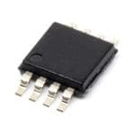
| 供应商器件封装 | 8-MSOP |
| 共模抑制比—最小值 | 88 dB |
| 关闭 | No Shutdown |
| 其它名称 | AD8052ARMZ-REEL7DKR |
| 包装 | Digi-Reel® |
| 压摆率 | 170 V/µs |
| 商标 | Analog Devices |
| 增益带宽生成 | 80 MHz |
| 增益带宽积 | - |
| 安装类型 | 表面贴装 |
| 安装风格 | SMD/SMT |
| 封装 | Reel |
| 封装/外壳 | 8-TSSOP,8-MSOP(0.118",3.00mm 宽) |
| 封装/箱体 | MSOP-8 |
| 工作温度 | -40°C ~ 125°C |
| 工作电源电压 | 3 V to 12 V |
| 工厂包装数量 | 1000 |
| 拓扑结构 | Voltage Feedback |
| 放大器类型 | 电压反馈 |
| 最大工作温度 | + 125 C |
| 最小工作温度 | - 40 C |
| 标准包装 | 1 |
| 电压-电源,单/双 (±) | 3 V ~ 12 V, ±1.5 V ~ 6 V |
| 电压-输入失调 | 1.8mV |
| 电压增益dB | 98 dB |
| 电流-电源 | 4.8mA |
| 电流-输入偏置 | 1.4µA |
| 电流-输出/通道 | 45mA |
| 电源电压-最大 | 12 V |
| 电源电压-最小 | 3 V |
| 电源电流 | 11 mA |
| 电路数 | 2 |
| 稳定时间 | 50 ns |
| 系列 | AD8052 |
| 视频文件 | http://www.digikey.cn/classic/video.aspx?PlayerID=1364138032001&width=640&height=505&videoID=2245193153001 |
| 转换速度 | 145 V/us at 5 V |
| 输入补偿电压 | 1.7 mV |
| 输出电流 | 45 mA |
| 输出类型 | 满摆幅 |
| 通道数量 | 2 Channel |


- 商务部:美国ITC正式对集成电路等产品启动337调查
- 曝三星4nm工艺存在良率问题 高通将骁龙8 Gen1或转产台积电
- 太阳诱电将投资9.5亿元在常州建新厂生产MLCC 预计2023年完工
- 英特尔发布欧洲新工厂建设计划 深化IDM 2.0 战略
- 台积电先进制程称霸业界 有大客户加持明年业绩稳了
- 达到5530亿美元!SIA预计今年全球半导体销售额将创下新高
- 英特尔拟将自动驾驶子公司Mobileye上市 估值或超500亿美元
- 三星加码芯片和SET,合并消费电子和移动部门,撤换高东真等 CEO
- 三星电子宣布重大人事变动 还合并消费电子和移动部门
- 海关总署:前11个月进口集成电路产品价值2.52万亿元 增长14.8%


PDF Datasheet 数据手册内容提取
Low Cost, High Speed, Rail-to-Rail Amplifiers AD8051/AD8052/AD8054 FEATURES PIN CONNECTIONS (TOP VIEWS) High speed and fast settling on 5 V AD8051 111500 MMHHzz,, −−33 ddBB bbaannddwwiiddtthh ((GG == ++11)) ((AADD88005514/) AD8052) –NICN 12 87 N+VCS VOUT 1 AD8051 5 +VS Sin15g40l5 en -Vss /usμepstp tsllliyen wogp treiamrtaeet itoon 0 .1% –+VINS N34C = NO CONNEC65T NVOCUT 01062-001 –+VINS 23 +– 4 –IN 01062-002 Figure 1. SOIC-8 (R) Figure 2. SOT-23-5 (RJ) Output swings to within 25 mV of either rail Input voltage range: −0.2 V to +4 V; V = 5 V S Video specifications (G = +2) OUT A 1 14 OUT D 0.1 dB gain flatness: 20 MHz; R = 150 Ω L AD8052 –IN A 2 13 –IN D Differential gain/phase: 0.03%/0.03° OUT1 1 8 +VS +IN A 3 12 +IN D Low distortion –IN1 2 –+ 7 OUT V+ 4 AD8054 11 V– Ou−Dt8srti0va ednsBd 4cin 5tgo m tloaAla, h d0a .d5rrm Vivo fenr ocicam p@ sa u1bp iMlpitHlyyz r, aRiLl s= ( 1A0D08 Ω05 1/AD8052) +–INV1S 34 –+ 65 –+IINN22 01062-003 O+–UIINNT BBB 567 1980 +O–IIUNNT CC C 01062-004 Drives 50 pF capacitive load (G = +1) (AD8051/AD8052) Figure 3. SOIC (R-8) and MSOP (RM-8) Figure 4. SOIC (R-14) and TSSOP (RU-14) Low power: 2.75 mA/amplifier (AD8054) Low power: 4.4 mA/amplifier (AD8051/AD8052) 5.0 APPLICATIONS G AAcntaivloeg f-itltoe-rdsi gital drivers GE SWIN 44..50 VGRSF = == – 521VkΩ TA 3.5 RL = 2kΩ CColoncsku bmuefrfe vri deo T VOL%) (V) 3.0 U5 PCCroDf eimssaiogninagl c saymsteermass K OUTPTHD ≤ 0. 22..05 A( CD/DVD ROMs PE 1.5 O- T 1.0 K- EA 0.5 P 00.1 FR1EQUENCY (MHz) 10 50 01062-005 Figure 5. Low Distortion Rail-to-Rail Output Swing GENERAL DESCRIPTION The AD8051 (single), AD8052 (dual), and AD8054 (quad) are The AD8051/AD8052/AD8054 are well suited for video low cost, high speed, voltage feedback amplifiers. The amplifiers electronics, cameras, video switchers, or any high speed portable operate on +3 V, +5 V, or ±5 V supplies at low supply current. equipment. Low distortion and fast settling make them ideal for They have true single-supply capability with an input voltage active filter applications. range extending 200 mV below the negative rail and within 1 V The AD8051/AD8052 in the 8-lead SOIC, the AD8052 in the of the positive rail. MSOP, the AD8054 in the 14-lead SOIC, and the 14-lead TSSOP Despite their low cost, the AD8051/AD8052/AD8054 provide packages are available in the extended temperature range of excellent overall performance and versatility. The output voltage −40°C to +125°C. swings to within 25 mV of each rail, providing maximum output dynamic range with excellent overdrive recovery. Rev. J Information furnished by Analog Devices is believed to be accurate and reliable. However, no responsibility is assumed by Analog Devices for its use, nor for any infringements of patents or other One Technology Way, P.O. Box 9106, Norwood, MA 02062-9106, U.S.A. rights of third parties that may result from its use. Specifications subject to change without notice. No license is granted by implication or otherwise under any patent or patent rights of Analog Devices. Tel: 781.329.4700 www.analog.com Trademarks and registered trademarks are the property of their respective owners. Fax: 781.461.3113 ©2009 Analog Devices, Inc. All rights reserved.
AD8051/AD8052/AD8054 TABLE OF CONTENTS Features .............................................................................................. 1 Circuit Description .................................................................... 16 Applications ....................................................................................... 1 Application Information ................................................................ 17 Pin Connections (Top Views) ......................................................... 1 Overdrive Recovery ................................................................... 17 General Description ......................................................................... 1 Driving Capacitive Loads .......................................................... 17 Revision History ............................................................................... 2 Layout Considerations ............................................................... 18 Specifications ..................................................................................... 3 Active Filters ............................................................................... 18 Absolute Maximum Ratings ............................................................ 9 Analog-to-Digital and Digital-to-Analog Applications ........ 19 Thermal Resistance ...................................................................... 9 Sync Stripper ............................................................................... 20 Maximum Power Dissipation ..................................................... 9 Single-Supply Composite Video Line Driver ......................... 20 ESD Caution .................................................................................. 9 Outline Dimensions ....................................................................... 21 Typical Performance Characteristics ........................................... 10 Ordering Guide .......................................................................... 23 Theory of Operation ...................................................................... 16 REVISION HISTORY 7/09—Rev. I to Rev. J 2/03—Rev. C to Rev. D Changes to Figure 22 ...................................................................... 12 Changes to General Description ..................................................... 1 Changes to Specifications ................................................................. 3 12/08—Rev. H to Rev. I Changes to Absolute Maximum Ratings ........................................ 6 Change to Settling Time to 0.1% Parameter, Table 1 ................... 3 1/03—Rev. B to Rev. C Updated Outline Dimensions ....................................................... 20 Changes to General Description ..................................................... 1 Changes to Pin Connections ............................................................ 1 12/07—Rev. G to Rev. H Changes to Specifications ................................................................. 2 Changes to Applications .................................................................. 1 Changes to Absolute Maximum Ratings ........................................ 9 Updated Outline Dimensions ....................................................... 21 Changes to Figure 2 ........................................................................... 9 Changes to Ordering Guide .......................................................... 23 Changes to Ordering Guide ............................................................. 9 5/06—Rev. F to Rev. G Updated Outline Dimensions ........................................................ 20 Updated Format .................................................................. Universal Changes to Features, Applications, and General Description ..... 1 Changes to Figure 15 ...................................................................... 12 Changes to the Ordering Guide .................................................... 22 9/04—Rev. E to Rev. F Changes to Ordering Guide ............................................................. 7 Changes to Figure 15 ...................................................................... 15 3/04—Rev. D to Rev. E Changes to General Description ..................................................... 2 Changes to Specifications ................................................................. 3 Changes to Ordering Guide ............................................................. 6 Rev. J | Page 2 of 24
AD8051/AD8052/AD8054 SPECIFICATIONS @ T = 25°C, V = 5 V, R = 2 kΩ to 2.5 V, unless otherwise noted. A S L Table 1. AD8051A/AD8052A AD8054A Parameter Conditions Min Typ Max Min Typ Max Unit DYNAMIC PERFORMANCE −3 dB Small Signal Bandwidth G = +1, V = 0.2 V p-p 70 110 80 150 MHz OUT G = −1, +2, V = 0.2 V p-p 50 60 MHz OUT Bandwidth for 0.1 dB Flatness G = +2, V = 0.2 V p-p, OUT R = 150 Ω to 2.5 V L R = 806 Ω (AD8051A/ 20 MHz F AD8052A) R = 200 Ω (AD8054A) 12 MHz F Slew Rate G = −1, V = 2 V step 100 145 140 170 V/μs OUT Full Power Response G = +1, V = 2 V p-p 35 45 MHz OUT Settling Time to 0.1% G = −1, V = 2 V step 50 40 ns OUT NOISE/DISTORTION PERFORMANCE Total Harmonic Distortion1 f = 5 MHz, V = 2 V p-p, −67 −68 dB C OUT G = +2 Input Voltage Noise f = 10 kHz 16 16 nV/√Hz Input Current Noise f = 10 kHz 850 850 fA/√Hz Differential Gain Error (NTSC) G = +2, R = 150 Ω to 2.5 V 0.09 0.07 % L R = 1 kΩ to 2.5 V 0.03 0.02 % L Differential Phase Error (NTSC) G = +2, R = 150 Ω to 2.5 V 0.19 0.26 Degrees L R = 1 kΩ to 2.5 V 0.03 0.05 Degrees L Crosstalk f = 5 MHz, G = +2 −60 −60 dB DC PERFORMANCE Input Offset Voltage 1.7 10 1.7 12 mV T − T 25 30 mV MIN MAX Offset Drift 10 15 μV/°C Input Bias Current 1.4 2.5 2 4.5 μA T − T 3.25 4.5 μA MIN MAX Input Offset Current 0.1 0.75 0.2 1.2 μA Open-Loop Gain R = 2 kΩ to 2.5 V 86 98 82 98 dB L T − T 96 96 dB MIN MAX R = 150 Ω to 2.5 V 76 82 74 82 dB L T − T 78 78 dB MIN MAX INPUT CHARACTERISTICS Input Resistance 290 300 kΩ Input Capacitance 1.4 1.5 pF Input Common-Mode Voltage Range −0.2 to −0.2 to V +4 +4 Common-Mode Rejection Ratio V = 0 V to 3.5 V 72 88 70 86 dB CM Rev. J | Page 3 of 24
AD8051/AD8052/AD8054 AD8051A/AD8052A AD8054A Parameter Conditions Min Typ Max Min Typ Max Unit OUTPUT CHARACTERISTICS Output Voltage Swing R = 10 kΩ to 2.5 V 0.015 to 0.03 to V L 4.985 4.975 R = 2 kΩ to 2.5 V 0.1 to 0.025 to 0.125 to 0.05 to V L 4.9 4.975 4.875 4.95 R = 150 Ω to 2.5 V 0.3 to 0.2 to 0.55 to 0.25 to V L 4.625 4.8 4.4 4.65 Output Current V = 0.5 V to 4.5 V 45 30 mA OUT T − T 45 30 mA MIN MAX Short-Circuit Current Sourcing 80 45 mA Sinking 130 85 mA Capacitive Load Drive G = +1 (AD8051/AD8052) 50 pF G = +2 (AD8054) 40 pF POWER SUPPLY Operating Range 3 12 3 12 V Quiescent Current/Amplifier 4.4 5 2.75 3.275 mA Power Supply Rejection Ratio ΔV = ±1 V 70 80 68 80 dB S OPERATING TEMPERATURE RANGE RJ-5 −40 +85 °C RM-8, R-8, RU-14, R-14 −40 +125 −40 +125 °C 1 Refer to Figure 19. Rev. J | Page 4 of 24
AD8051/AD8052/AD8054 @ T = 25°C, V = 3 V, R = 2 kΩ to 1.5 V, unless otherwise noted. A S L Table 2. AD8051A/AD8052A AD8054A Parameter Conditions Min Typ Max Min Typ Max Unit DYNAMIC PERFORMANCE −3 dB Small Signal Bandwidth G = +1, V = 0.2 V p-p 70 110 80 135 MHz OUT G = −1, +2, V = 50 65 MHz OUT 0.2 V p-p Bandwidth for 0.1 dB Flatness G = +2, V = 0.2 V p-p, OUT R = 150 Ω to 2.5 V L R = 402 Ω (AD8051A/ 17 MHz F AD8052A) R = 200 Ω (AD8054A) 10 MHz F Slew Rate G = −1, V = 2 V step 90 135 110 150 V/μs OUT Full Power Response G = +1, V = 1 V p-p 65 85 MHz OUT Settling Time to 0.1% G = −1, V = 2 V step 55 55 ns OUT NOISE/DISTORTION PERFORMANCE Total Harmonic Distortion1 f = 5 MHz, V = 2 V p-p, −47 −48 dB C OUT G = −1, R = 100 Ω to 1.5 V L Input Voltage Noise f = 10 kHz 16 16 nV/√Hz Input Current Noise f = 10 kHz 600 600 fA/√Hz Differential Gain Error (NTSC) G = +2, V = 1 V CM R = 150 Ω to 1.5 V 0.11 0.13 % L R = 1 kΩ to 1.5 V 0.09 0.09 % L Differential Phase Error (NTSC) G = +2, V = 1 V CM R = 150 Ω to 1.5 V 0.24 0.3 Degrees L R = 1 kΩ to 1.5 V 0.10 0.1 Degrees L Crosstalk f = 5 MHz, G = +2 −60 −60 dB DC PERFORMANCE Input Offset Voltage 1.6 10 1.6 12 mV T − T 25 30 mV MIN MAX Offset Drift 10 15 μV/°C Input Bias Current 1.3 2.6 2 4.5 μA T − T 3.25 4.5 μA MIN MAX Input Offset Current 0.15 0.8 0.2 1.2 μA Open-Loop Gain R = 2 kΩ 80 96 80 96 dB L T − T 94 94 dB MIN MAX R = 150 Ω 74 82 72 80 dB L T − T 76 76 dB MIN MAX INPUT CHARACTERISTICS Input Resistance 290 300 kΩ Input Capacitance 1.4 1.5 pF Input Common-Mode Voltage Range −0.2 to −0.2 to V +2 +2 Common-Mode Rejection Ratio V = 0 V to 1.5 V 72 88 70 86 dB CM Rev. J | Page 5 of 24
AD8051/AD8052/AD8054 AD8051A/AD8052A AD8054A Parameter Conditions Min Typ Max Min Typ Max Unit OUTPUT CHARACTERISTICS Output Voltage Swing R = 10 kΩ to 1.5 V 0.01 to 0.025 to V L 2.99 2.98 R = 2 kΩ to 1.5 V 0.0.75 to 0.02 to 0.1 to 0.35 to V L 2.9 2.98 2.9 2.965 R = 150 Ω to 1.5 V 0.2 to 0.125 to 0.35 to 0.15 to V L 2.75 2.875 2.55 2.75 Output Current V = 0.5 V to 2.5 V 45 25 mA OUT T − T 45 25 mA MIN MAX Short-Circuit Current Sourcing 60 30 mA Sinking 90 50 mA Capacitive Load Drive G = +1 (AD8051/AD8052) 45 pF G = +2 (AD8054) 35 pF POWER SUPPLY Operating Range 3 12 3 12 V Quiescent Current/Amplifier 4.2 4.8 2.625 3.125 mA Power Supply Rejection Ratio ΔV = 0.5 V 68 80 68 80 dB S OPERATING TEMPERATURE RANGE RJ-5 −40 +85 °C RM-8, R-8, RU-14, R-14 −40 +125 −40 +125 °C 1 Refer to Figure 19. Rev. J | Page 6 of 24
AD8051/AD8052/AD8054 @ T = 25°C, V = ±5 V, R = 2 kΩ to ground, unless otherwise noted. A S L Table 3. AD8051A/AD8052A AD8054A Parameter Conditions Min Typ Max Min Typ Max Unit DYNAMIC PERFORMANCE −3 dB Small Signal Bandwidth G = +1, V = 0.2 V p-p 70 110 85 160 MHz OUT G = −1, +2, V = 0.2 V p-p 50 65 MHz OUT Bandwidth for 0.1 dB Flatness G = +2, V = 0.2 V p-p, OUT R = 150 Ω, L R = 1.1 kΩ (AD8051A/ 20 MHz F AD8052A) R = 200 Ω (AD8054A) 15 MHz F Slew Rate G = −1, V = 2 V step 105 170 150 190 V/μs OUT Full Power Response G = +1, V = 2 V p-p 40 50 MHz OUT Settling Time to 0.1% G = −1, V = 2 V step 50 40 MHz OUT NOISE/DISTORTION PERFORMANCE Total Harmonic Distortion f = 5 MHz, V = 2 V p-p, −71 −72 dB C OUT G = +2 Input Voltage Noise f = 10 kHz 16 16 nV/√Hz Input Current Noise f = 10 kHz 900 900 fA/√Hz Differential Gain Error (NTSC) G = +2, R = 150 Ω 0.02 0.06 % L R = 1 kΩ 0.02 0.02 % L Differential Phase Error (NTSC) G = +2, R = 150 Ω 0.11 0.15 Degrees L R = 1 kΩ 0.02 0.03 Degrees L Crosstalk f = 5 MHz, G = +2 −60 −60 dB DC PERFORMANCE Input Offset Voltage 1.8 11 1.8 13 mV T − T 27 32 mV MIN MAX Offset Drift 10 15 μV/°C Input Bias Current 1.4 2.6 2 4.5 μA T − T 3.5 4.5 μA MIN MAX Input Offset Current 0.1 0.75 0.2 1.2 μA Open-Loop Gain R = 2 kΩ 88 96 84 96 dB L T − T 96 96 dB MIN MAX R = 150 Ω 78 82 76 82 dB L T − T 80 80 dB MIN MAX INPUT CHARACTERISTICS Input Resistance 290 300 kΩ Input Capacitance 1.4 1.5 pF Input Common-Mode Voltage Range −5.2 to −5.2 to V +4 +4 Common-Mode Rejection Ratio V = −5 V to +3.5 V 72 88 70 86 dB CM OUTPUT CHARACTERISTICS Output Voltage Swing R = 10 kΩ −4.98 to −4.97 to V L +4.98 +4.97 R = 2 kΩ −4.85 to −4.97 to −4.8 to −4.9 to V L +4.85 +4.97 +4.8 +4.9 R = 150 Ω −4.45 to −4.6 to −4.0 to −4.5 to V L +4.3 +4.6 +3.8 +4.5 Output Current V = −4.5 V to +4.5 V 45 30 mA OUT T − T 45 30 mA MIN MAX Short-Circuit Current Sourcing 100 60 mA Sinking 160 100 mA Capacitive Load Drive G = +1 (AD8051/AD8052) 50 pF G = +2 (AD8054) 40 pF Rev. J | Page 7 of 24
AD8051/AD8052/AD8054 AD8051A/AD8052A AD8054A Parameter Conditions Min Typ Max Min Typ Max Unit POWER SUPPLY Operating Range 3 12 3 12 V Quiescent Current/Amplifier 4.8 5.5 2.875 3.4 mA Power Supply Rejection Ratio ΔV = ±1 68 80 68 80 dB S OPERATING TEMPERATURE RANGE RJ-5 −40 +85 °C RM-8, R-8, RU-14, R-14 −40 +125 −40 +125 °C Rev. J | Page 8 of 24
AD8051/AD8052/AD8054 ABSOLUTE MAXIMUM RATINGS Table 4. MAXIMUM POWER DISSIPATION Parameter Ratings The maximum power that can be safely dissipated by the Supply Voltage 12.6 V AD8051/AD8052/AD8054 is limited by the associated rise in Internal Power Dissipation1 junction temperature. The maximum safe junction temperature SOIC Packages Observe power for plastic encapsulated devices is determined by the glass derating curves transition temperature of the plastic, approximately 150°C. SOT-23 Package Observe power Temporarily exceeding this limit can cause a shift in parametric derating curves performance due to a change in the stresses exerted on the die MSOP Package Observe power by the package. Exceeding a junction temperature of 175°C for derating curves an extended period can result in device failure. TSSOP Package Observe power derating curves While the AD8051/AD8052/AD8054 are internally short- Input Voltage (Common Mode) ±VS circuit protected, this cannot be sufficient to guarantee that the Differential Input Voltage ±2.5 V maximum junction temperature (150°C) is not exceeded under Output Short-Circuit Duration Observe power all conditions. To ensure proper operation, it is necessary to derating curves observe the maximum power derating curves. Storage Temperature Range (R) −65°C to +150°C 2.5 Operating Temperature Range (A Grade) −40°C to +125°C Lead Temperature (Soldering 10 sec) 300°C W) N ( 2.0 SOIC-14 O 1 See Table 5. TI TSSOP-14 A Stresses above those listed under Absolute Maximum Ratings SIP 1.5 SOIC-8 S may cause permanent damage to the device. This is a stress DI R rating only; functional operation of the device at these or any WE O 1.0 other conditions above those indicated in the operational P M MSOP-8 section of this specification is not implied. Exposure to absolute U M maximum rating conditions for extended periods may affect AXI 0.5 SOT-23-5 M device reliability. TSpHecEiRficMatAioLn RisE foSrI SdeTvAicNe CinE f ree air. 0–55 –35 –15AMB5IENT1 T5EMP3E5RATU55RE (°C75) 95 115 01062-006 Figure 6. Maximum Power Dissipation vs. Temperature for AD8051/AD8052/AD8054 Table 5. Thermal Resistance Package Type θ Unit ESD CAUTION JA 8-Lead SOIC 125 °C/W 5-Lead SOT-23 180 °C/W 8-Lead MSOP 150 °C/W 14-Lead SOIC 90 °C/W 14-Lead TSSOP 120 °C/W Rev. J | Page 9 of 24
AD8051/AD8052/AD8054 TYPICAL PERFORMANCE CHARACTERISTICS 3 5 21 GRF = = + 22kΩ 43 GRVSFA I=AN S5 A VSSH SOHWONWN GRF = = + 22kΩ GRF = = + 01 N (dB) 0 G = +5 N (dB) 21 RVOL U=T 5 =k Ω0.2V p-p GAI –1 RF = 2kΩ G = +1 GAI 0 ALIZED ––32 GRF = = + 21k0Ω RF = 0 ALIZED ––21 G = +10 ORM –4 VS = 5V ORM –3 RF = 2kΩ N GAIN AS SHOWN N –4 –5 RF AS SHOWN –6 RVOL U=T 2 =k Ω0.2V p-p ––56 GRF = = + 25kΩ –70.1 1 FREQUENC1Y0 (MHz) 100 500 01062-007 –1700k 1M FREQUEN1C0YM (Hz) 100M 500M 01062-010 Figure 7. AD8051/AD8052 Normalized Gain vs. Frequency; VS = 5 V Figure 10. AD8054 Normalized Gain vs. Frequency; VS = 5 V 3 6 21 VVGRSOL=UA=+TS21=kSΩ0H.2OVWpN-p VS = +3V VS = +5V 54 CGRVOLL= U==+T 251=kpΩ0F.2Vp-p ++35VV 0 3 ±5V B) –1 VS = ±5V B) 2 d d N ( –2 N ( 1 AI AI G –3 G 0 –4 –1 ±5V –5 –2 +3V –6 –3 +5V –70.1 1 FREQUENC1Y0 (MHz) 100 500 01062-008 –1400k 1M FREQUEN1C0YM (Hz) 100M 500M 01062-011 Figure 8. AD8051/AD8052 Gain vs. Frequency vs. Supply Figure 11. AD8054 Gain vs. Frequency vs. Supply 3 4 VS = 5V +85°C 2 3 RL = 2kΩTO 2.5V +25°C 1 –40°C 2 CGL = = + 51pF –40°C 0 VOUT = 0.2V p-p 1 +85°C dB) –1 +25°C dB) 0 N ( –2 N ( AI AI–1 G –3 G –2 –4 VS= 5V G=+1 –5 RL=2kΩ –3 VOUT=0.2Vp-p –6 TEMPERATURE AS SHOWN –4 –70.1 1 FREQUEN1C0Y (MHz) 100 500 01062-009 –51 F1R0EQUENCY (MHz) 100 500 01062-012 Figure 9. AD8051/AD8052 Gain vs. Frequency vs. Temperature Figure 12. AD8054 Gain vs. Frequency vs. Temperature Rev. J | Page 10 of 24
AD8051/AD8052/AD8054 6.3 6.3 6.2 6.2 6.1 6.1 B) 6.0 B) 6.0 SS (d 5.9 SS (d 5.9 E E N N AT 5.8 AT 5.8 L L N F 5.7 N F 5.7 GAI 5.6 GVS = = + 52V GAI 5.6 VRSF == 52V00Ω 5.5 RL = 150Ω 5.5 RL = 150Ω RF = 806Ω G = +2 5.4 VOUT = 0.2V p-p 5.4 VOUT = 0.2V p-p 5.30.1 1FREQUENCY (MHz)10 100 01062-013 5.31 FREQUE1N0CY (MHz) 100 01062-016 Figure 13. AD8051/AD8052 0.1 dB Gain Flatness vs. Frequency; G = +2 Figure 16. AD8054 0.1 dB Gain Flatness vs. Frequency; G = +2 9 9 8 VVSO U=T + =5 V2V p-p 8 VVSO U=T + =5 V2V p-p 7 7 6 6 B) 5 B) 5 GAIN (d 34 VS = ±5V GAIN (d 34 VVSO U=T ± =5 V4V p-p 2 VGS = A +S2 SHOWN VOUT = 4V p-p 2 VGS = A +S2 SHOWN 1 RF = 2kΩ 1 RF = 2kΩ RL = 2kΩ RL = 2kΩ 0 VOUT AS SHOWN 0 VOUT AS SHOWN –10.1 1 FREQUENC1Y0 (MHz) 100 500 01062-014 –10.1 1 FREQUENC1Y0 (MHz) 100 500 01062-017 Figure 14. AD8051/AD8052 Large Signal Frequency Response; G = +2 Figure 17. AD8054 Large Signal Frequency Response; G = +2 80 80 70 VS = 5V 70 VS = 5V RL = 2kΩ RL = 2kΩ 60 60 CL = 5pF GAIN (dB)4500 GAIN N (Degrees) GAIN (dB)4500 GAIN N (Degrees) OPEN-LOOP 123000 PHASE 5M0A° RPGHIANSE 0––4950 HASE MARGI OPEN-LOOP 123000 PHASE 4M5A° RPGHIANSE 91108305HASE MARGI 0 –135P 0 45 P –10 –180 –10 0 –200.01 0.1 FREQ1UENCY (MH1z0) 100 500 01062-015 –2030k 100k 1FMREQUENCY1 (0HMz) 100M 500M 01062-018 Figure 15. AD8051/AD8052 Open-Loop Gain and Phase vs. Frequency Figure 18. AD8054 Open-Loop Gain and Phase Margin vs. Frequency Rev. J | Page 11 of 24
AD8051/AD8052/AD8054 –20 1000 VOUT = 2V p-p VS = 3V, G = –1 VS = 5V c) –30 RF = 2kΩ, RL = 100Ω dB VS = 5V, G = +2 ORTION ( ––5400 VRSL == 51V00, ΩG = +1RF = 2kΩ, RL = 100Ω nV/√Hz)100 ONIC DIST ––7600 GE NOISE ( RM –80 VS = 5V, G = +1 TA 10 HA RL = 2kΩ OL AL –90 VS = 5V, G = +2 V OT RF = 2kΩ, RL = 2kΩ T–100 –1101 FUNDA2MENTAL 3FREQU4ENCY5 (MHz6) 7 8 910 01062-019 110 100 1kFREQU1E0NkCY (Hz1)00k 1M 10M 01062-022 Figure 19. Total Harmonic Distortion Figure 22. Input Voltage Noise vs. Frequency –30 100 VS = 5V –40 –50 10MHz Bc) –60 √Hz) NIC (d –70 E (pA/10 RMO –80 5MHz NOIS HA –90 NT RST –100 1MHz RRE 1 WO–110 VS = 5V CU RL = 2kΩ –120 G = +2 –130 –1400 0.5 1.0 1O.5UTP2U.0T VO2L.5TAG3E.0 (V p3-.p5) 4.0 4.5 5.0 01062-020 0.110 100 1kFREQU1E0NkCY (Hz1)00k 1M 10M 01062-023 Figure 20. Worst Harmonic vs. Output Voltage Figure 23. Input Current Noise vs. Frequency 0.10 0.10 DIFFERENTIALGAIN ERROR (%) –––00000000........0000000062486420 0NVRTSFS 1==C0 25 SVkΩ,U G,B2 R0 S=LC +AR2SI3B 0SEHRO (43W0.5N8MH50z) 60 R7RL0 L= =1 5180k0ΩΩ 90 100 DIFFERENTIALGAIN ERROR (%)––0000....10000550 1NVRSTSFTS ==C 252 SNVkΩDU, G,B R S3=LRC D+AR2SIB 4SETHRHO (3W5.T5NH8MH6TzH) 7TRHLR L=8 =T1H 510kΩΩ9TH 10TH11TH DIFFERENTIALPHASE ERROR (Degrees) –––––00000000........0112200150505500 0 VRSF 1==0 25VkΩ, G,2 R0 =LM +AO2SD3 0USLHAOT4WI0NNG R5A0MP R6L0EL V=E 1Lk7R Ω0(ILR =E )18500Ω 90 100 01062-021 DIFFERENTIALPHASE ERROR (Degrees) –––0000000.......1232103 1VRSSFT == 252NVkΩD, G, R 3=LMR D+AO2SD 4USTLHHAOTW5ITNRNHGL R=6 AT1HMkΩP 7LTEHVE8LT H(IRE9T)RHL =1 01T5H0Ω11TH 01062-024 Figure 21. AD8051/AD8052 Differential Gain and Phase Errors Figure 24. AD8054 Differential Gain and Phase Errors Rev. J | Page 12 of 24
AD8051/AD8052/AD8054 –10 –10 VS = 5V VS = ±5V –20 RF = 2kΩ –20 RF = 1kΩ –30 RVOL U=T 2 =k Ω2V p-p –30 RVOL U=TA =S 2 SVH pO-pWN –40 B)–40 B) STALK (d––5600 STALK (d ––5600 RL = 100Ω OS OS –70 CR–70 CR RL = 1kΩ –80 –80 –90 –90 –100 –1000.1 1 FREQUENC1Y0 (MHz) 100 500 01062-025 –1100.1 1 FREQUENC1Y0 (MHz) 100 500 01062-028 Figure 25. AD8052 Crosstalk (Output-to-Output) vs. Frequency Figure 28. AD8054 Crosstalk (Output-to-Output) vs. Frequency 0 20 –10 VS = 5V 10 VS = 5V –20 0 –30 –10 B) –40 B) –20 –PSRR d d R ( –50 R ( –30 R R M S C –60 P –40 +PSRR –70 –50 –80 –60 –90 –70 –1000.03 0.1 F1REQUENCY (1M0Hz) 100 500 01062-026 –800.01 0.1 FREQ1UENCY (MH1z0) 100 500 01062-029 Figure 26. CMRR vs. Frequency Figure 29. PSRR vs. Frequency 100.000 70 VS=5V VS = 5V 31.000 G = +1 G = –1 60 RL = 2kΩ Ω)10.000 ns) E ( % ( 50 ESISTANC 31..100000 ME TO 0.1 40 AD80A5D18/A05D48052 TPUT R 0.310 LING TI 30 U T 20 O 0.100 T E S 0.031 10 0.0100.1 1 FREQUENC1Y0 (MHz) 100 500 01062-027 00.5 1.0INPUT STEP (V p-p1).5 2.0 01062-030 Figure 27. Closed-Loop Output Resistance vs. Frequency Figure 30. Settling Time vs. Input Step Rev. J | Page 13 of 24
AD8051/AD8052/AD8054 1.0 1.000 VS = 5V VOH = +85°C VS = 5V N VOLTAGE (V)0000....9786 VOHV =O –H4 =0 °+C25°C VOL = +85°C N VOLTAGE (V)000...876752505 +5V –+ V5VO H– (V+O25H° C(+)125°C) UTPUT SATURATIO0000....3425 VOL = –40°VCOL = +25°C UTPUT SATURATIO000...523057005 +5V – VOH (–40°C) VOL (+125°C) O0.1 O0.125 VOL (+25°C) VOL (–40°C) 00 5 10 15 20 25L3O0AD35 C4U0RR4E5N5T0 (m55A)60 65 7075 80 85 01062-031 00 3 6 9LOA1D2 CUR1R5ENT1 8(mA)21 24 27 30 01062-033 Figure 31. AD8051/AD8052 Output Saturation Voltage vs. Load Current Figure 33. AD8054 Output Saturation Voltage vs. Load Current 100 RL = 2kΩ 90 B) d N ( AI RL = 150Ω G P 80 O O L N- E P O 70 VS = 5V 600 0.5 1.0 1.5OUT2P.0UT V2O.5LTA3G.0E (V3).5 4.0 4.5 5.0 01062-032 Figure 32. Open-Loop Gain vs. Output Voltage Rev. J | Page 14 of 24
AD8051/AD8052/AD8054 VIN = 0.1V p-p VS = 5V G = +1 G = –1 RL = 2kΩ RF = 2kΩ VS = 3V 5.0 RL = 2kΩ S S LT1.5 LT 2.5 O O V V 20mV 20ns 01062-034 1V 2µs 01062-037 Figure 34. 100 mV Step Response, G = +1 Figure 37. Output Swing; G = −1, RL = 2 kΩ VS = 5V VS = 5V G = +1 G = +1 RL = 2kΩ RL = 2kΩ 2.6 2.55 S S OLT2.5 OLT2.50 V V 2.4 2.45 50mV 20ns 01062-035 50mV 40ns 01062-038 Figure 35. AD8051/AD8052 200 mV Step Response; VS = 5 V, G = +1 Figure 38. AD8054 100 mV Step Response; VS = 5 V, G = +1 4.5 VIN = 1V p-p 4 VS = ±5V G = +2 G = +1 RL = 2kΩ 3 RL = 2kΩ VS = 5V 3.5 2 1 OLTS 2.5 OLTS V V –1 1.5 –2 –3 0.5 500mV 20ns 01062-036 –4 1V 20ns 01062-039 Figure 36. Large Signal Step Response; VS = 5 V, G = +2 Figure 39. Large Signal Step Response; VS = ±5 V, G = +1 Rev. J | Page 15 of 24
AD8051/AD8052/AD8054 THEORY OF OPERATION CIRCUIT DESCRIPTION The inputs of the device can handle voltages from −0.2 V below the negative rail to within 1 V of the positive rail. Exceeding The AD8051/AD8052/AD8054 are fabricated on the Analog these values do not cause phase reversal; however, the input Devices, Inc. proprietary eXtra-Fast Complementary Bipolar ESD devices begin to conduct if the input voltages exceed the (XFCB) process, which enables the construction of PNP and rails by greater than 0.5 V. During this overdrive condition, the NPN transistors with similar fTs in the 2 GHz to 4 GHz region. output stays at the rail. The process is dielectrically isolated to eliminate the parasitic and latch-up problems caused by junction isolation. These The rail-to-rail output range of the AD8051/AD8052/AD8054 features allow the construction of high frequency, low distortion is provided by a complementary common emitter output stage. amplifiers with low supply currents. This design uses a differential High output drive capability is provided by injecting all output output input stage to maximize bandwidth and headroom (see stage predriver currents directly into the bases of the output Figure 40). The smaller signal swings required on the first stage devices Q8 and Q36. Biasing of Q8 and Q36 is accomplished by outputs (nodes SIP, SIN) reduce the effect of nonlinear currents I8 and I5, along with a common-mode feedback loop (not due to junction capacitances and improve the distortion per- shown). This circuit topology allows the AD8051/AD8052 to formance. This design achieves harmonic distortion of −80 dBc drive 45 mA of output current and allows the AD8054 to drive @ 1 MHz into 100 Ω with V = 2 V p-p (gain = +1) on a 30 mA of output current with the outputs within 0.5 V of the OUT single 5 V supply. supply rails. VCC R26 I10 R39 I2 I3 Q25 Q50 I9 Q36 Q4 Q5 Q51 Q39 I5 Q40 Q23 VEE R15 R2 VINP Q13 Q1 VEE Q22Q7 R23 R27 Q31 C3 VOUT Q21 Q27 VINN SIP SIN C9 Q2 Q11 Q8 Q3 Q24 Q47 I11 I8 VEE C7 R5 R21 R3 I7 VCC 01062-045 Figure 40. AD8051/AD8052 Simplified Schematic Rev. J | Page 16 of 24
AD8051/AD8052/AD8054 APPLICATION INFORMATION OVERDRIVE RECOVERY VS = 5V Overdrive of an amplifier occurs when the output and/or input G = +1 range is exceeded. The amplifier must recover from this over- RL = 2kΩ CL = 50pF drive condition. As shown in Figure 41, the AD8051/AD8052/ 2.60 AD8054 recover within 60 ns from negative overdrive and 2.55 S within 45 ns from positive overdrive. LT2.50 O V 2.45 VS = ±5V 2.40 G = +5 INPUT 1V/DIV RF = 2kΩ RL = 2kΩ S OUTPUT 2V/DIV 50mV 100ns 01062-042 LT Figure 43. AD8051/AD8052 200 mV Step Response; CL = 50 pF O V 10000 VS = 5V ≤ 30% OVERSHOOT V/DIVAS SHOWN 100ns 01062-040 pF)1000 RS = 3Ω Figure 41. Overdrive Recovery D ( RS = 0Ω A O DRIVING CAPACITIVE LOADS L E 100 V Consider the AD8051/AD8052 in a closed-loop gain of +1 with ACITI RG RF +V = 5 V and a load of 2 kΩ in parallel with 50 pF. Figure 42 P andS Figure 43 show their frequency and time domain responses, CA 10 100mVIVN RS VOUT respectively, to a small-signal excitation. The capacitive load STEP 50Ω CL drive of the AD8051/AD8052/AD8054 can be increased by aandddi Fnigg ua rleo w45 v sahluoew r tehsies teofrfe icnt soefr aie sse wriietsh r tehseis tlooar do.n F tighue rcea 4p4a c i- 11 2 3 ACL (V/V)4 5 6 01062-043 tive drive for varying voltage gains. As the closed-loop gain is Figure 44. AD8051/AD8052 Capacitive Load Drive vs. Closed-Loop Gain increased, the larger phase margin allows for larger capacitive loads with less peaking. Adding a series resistor with lower 1000 closed-loop gains accomplishes the same effect. For large VS = 5V capacitive loads, the frequency response of the amplifier is ≤ 30% OVERSHOOT dominated by the roll-off of the series resistor and the load capacitance. F) RS = 10Ω p D ( 8 OA RS = 0Ω L 6 E 100 V 4 CITI 2 APA RG RF N (dB) –20 C 10S0TmVEIVPN 50Ω RS CLVOUT AI G –––468 CVGRSLL = === + 5521V0kΩpF Fi1g0u1re 45. AD80254 Capacit3iveA CLLo (aVd/V D)r4ive vs. Close5d-Loop Ga6in 01062-044 –10 VOUT = 200mV p-p –120.1 1 FREQUENC1Y0 (MHz) 100 500 01062-041 Figure 42. AD8051/AD8052 Closed-Loop Frequency Response; CL = 50 pF Rev. J | Page 17 of 24
AD8051/AD8052/AD8054 LAYOUT CONSIDERATIONS noise bandwidth of the analog signal before analog-to-digital conversion. The specified high speed performance of the AD8051/AD8052/ AD8054 requires careful attention to board layout and component Note that the unused amplifier’s inputs should be tied to ground. selection. Proper RF design techniques and low parasitic R6 1kΩ component selection are necessary. C1 The PCB should have a ground plane covering all unused 50pF portions of the component side of the board to provide a low R2 13 impedance path. The ground plane should be removed from the R1 2kΩ 2Rk4Ω 5C0p2F 12 14 area near the input pins to reduce parasitic capacitance. VIN 3kΩ 2 1 2Rk3Ω 6 R5 3 7 2kΩ 9 Chip capacitors should be used for supply bypassing. One end 5 8 AD8054 10 should be connected to the ground plane and the other within AD8054 AD8054 3ta mntmalu omf e ealcehct proolwyteirc pcianp.a Acinto ard sdhiotiuolnda bl ela crogne n(4e.c7t eμdF i nto p 1a0r aμlFle)l , BFIALNTDE-RP AOSUSTPUT 01062-046 but not necessarily so close, to supply current for fast, large Figure 46. 2 MHz Biquad Band-Pass Filter Using AD8054 signal changes at the output. The frequency response of the circuit is shown in Figure 47. The feedback resistor should be located close to the inverting 0 input pin to keep the parasitic capacitance at this node to a minimum. Parasitic capacitance of less than 1 pF at the inverting –10 input can significantly affect high speed performance. Stripline design techniques should be used for long signal traces (greater than about 25 mm). These should be designed with a N (dB)–20 characteristic impedance of 50 Ω or 75 Ω and be properly AI G terminated at each end. –30 ACTIVE FILTERS Active filters at higher frequencies require wider bandwidth op –40 amps to work effectively. Excessive phase shift produced by lpoewrfeorr fmreaqnuceen. cy op amps can significantly affect active filter 10k 100k FREQUE1MNCY (Hz) 10M 100M 01062-047 Figure 47. Frequency Response of 2 MHz Band-Pass Biquad Filter Figure 46 shows an example of a 2 MHz biquad bandwidth filter that uses three op amps of an AD8054. Such circuits are sometimes used in medical ultrasound systems to lower the Rev. J | Page 18 of 24
AD8051/AD8052/AD8054 ANALOG-TO-DIGITAL AND DIGITAL-TO-ANALOG reduced to −60.18 dB and the ADC operated with 8.46 ENOBs APPLICATIONS as shown in Figure 49. The inclusion of the AD8051 in the circuit did not worsen the distortion performance of the AD9201. Figure 50 is a schematic showing the AD8051 used as a driver for an AD9201, a 10-bit, 20 MSPS, dual analog-to-digital 10 FUND PART# 0 converter. This converter is designed to convert I and Q signals in 0 FFTSIZE8192 –10 FCLK 20.0MHz communications systems. In this application, only the I channel FUND 998.5kHz –20 VIN –0.51dB is being driven. The I channel is enabled by applying a logic –30 THD –68.13 high to SELECT (Pin 13). dB)–40 SNR 54.97 The AD8051 is running from a dual supply and is configured UDE (–50 ESNINOABD584.8.706 foourt pau gta iisn 2 o Vf + p2-.p T, hweh iinchpu ist stihgen mal aixs itmerummin iantpeudt irna n50g eΩ o fa nthde t he AMPLIT––6700 2ND 3RD 4TH 5TH 6TH 7TH 8TH 9TH 23SNRFDDDR 7––177.466..50636 –80 4TH –76.35 AD9201. The 22 Ω series resistor limits the maximum current –90 5TH –79.05 6TH –80.36 that flows and helps to lower the distortion of the ADC. –100 7TH –75.08 –110 8TH –88.12 The AD9201 has differential inputs for each channel. These are dcoensingencatteedd ttoh eV AR EaFn d(P Bin in 2p2u)t, sw. Thihceh Bsu inpppulitess oaf p eoascihti vceh arnefneerle narcee –1200 1 2 3 FR4EQUEN5CY (M6Hz) 7 8 9 109TH –77.87 01062-049 Figure 48. FFT Plot for AD8051 Driving the AD9201 at 1 MHz of 2.5 V. Each of the B inputs has a small low-pass filter that also helps to reduce distortion. 10 The output of the op amp is ac-coupled into INA-I (Pin 16) via FUND PART# 0 0 FFTSIZE8192 two parallel capacitors to provide good high frequency and low –10 FCLK 20.0MHz FUND 9.5MHz frequency coupling. The 1 kΩ resistor references the signal to –20 VIN –0.44dB VREF that is applied to INB-I. Thus, INA-I swings both positive –30 THD –57.08 B) SNR 54.65 and negative with respect to the bias voltage applied to INB-I. DE (d––4500 SEINNOABD 582.4.669 Wdigitihta tl hoeu stpamutp wliansg a cnloalcykz erdu nwniitnhg a a dt i2g0it Mal SaPnaSl,y tzheer .a Tnwaloo gin-tpou-t AMPLITU––6700 2ND 4TH 6TH 8TH 7TH 5TH 3RD S23NRFDDDR 6––066.001..12883 frequencies were used, 1 MHz and 9.5 MHz, which is just short –80 4TH –82.01 5TH –78.83 of the Nyquist frequency. These signals were well filtered to –90 6TH –81.28 minimize any harmonics. –100 7TH –77.28 –110 8TH –84.54 F1 iMguHrez 4a8n ashloogw isn tphuet .F TFhTe rSeFspDoRn sise 7o1f .t6h6e dABD, aCn dfo trh teh ea ncaalsoeg o-tfo a- –1200 1 2 3 FRE4QUEN5CY (M6Hz) 7 8 9 109TH –92.78 01062-050 digital is producing 8.8 ENOB (effective number of bits). When Figure 49. FFT Plot for AD8051 Driving the AD9201 at 9.5 MHz the analog frequency was raised to 9.5 MHz, the SFDR was 15 SLEEP CLOCK 14 0.33µF 22Ω 16 INA-I SELECT 13 +VDD +5V 10pF 1kΩ 22Ω 17 INB-I 0.1µF 10µF 0.01µF 10pF AD9201 DATA OUT 3 7 22Ω 0.1µF 10µF 0.1µF 18 REFT-I D9 12 50Ω AD8051 6 0.1µF 19 REFB-I D8 11 20 AVSS D7 10 2 1kΩ 4 21 REFSENSE D6 9 22 VREF D5 8 0.1µF 10µF 10µF 0.1µF D4 7 –5V +5V 23 AVDD 10µF 0.1µF D3 6 1kΩ 24 REFB-Q D2 5 0.1µF 10µF 0.1µF 25 REFT-Q D1 4 0.1µF D0 3 22Ω 26 INB-Q DVDD 2 +5V 10pF DVSS 1 0.1µF 10µF 22Ω 27 INA-Q 10pF 28 CHIP–SELECT 01062-048 Figure 50. The AD8051 Driving an AD9201, a 10-Bit, 20 MSPS Analog-to-Digital Converter Rev. J | Page 19 of 24
AD8051/AD8052/AD8054 SYNC STRIPPER dynamic swing requirements are a signal that is mostly low but goes high with a duty cycle that is a small fraction of a percent, Synchronizing pulses are sometimes carried on video signals so and the other extreme defined by the opposite condition. as not to require a separate channel to carry the synchronizing information. However, for some functions, such as analog-to- The worst case of composite video is not quite this demanding. digital conversion, it is not desirable to have the sync pulses on One bounding condition is a signal that is mostly black for an the video signal. These pulses reduce the dynamic range of the entire frame but has a white (full amplitude) minimum width video signal and do not provide any useful information for such spike at least once in a frame. a function. The other extreme is for a full white video signal. The blanking A sync stripper removes the synchronizing pulses from a video intervals and sync tips of such a signal have negative-going signal while passing all the useful video information. Figure 51 excursions in compliance with the composite video specifications. shows a practical single-supply circuit that uses only a single The combination of horizontal and vertical blanking intervals AD8051. It is capable of directly driving a reverse terminated limit such a signal to being at the highest (white) level for a video line. maximum of about 75% of the time. VIDEOWITHSYNC VIDEO WITHOUT SYNC As a result of the duty cycles between the two extremes previously presented, a 1 V p-p composite video signal that is multiplied by a gain of 2 requires about 3.2 V p-p of dynamic voltage swing at the output for an op amp to pass a composite VBLANK 0.4V GROUND video signal of arbitrarily varying duty cycle without distortion. GROUND 3V OR 5V Some circuits use a sync tip clamp to hold the sync tips at a + relatively constant level to lower the amount of dynamic signal 0.1µF 10µF swing required. However, these circuits can have artifacts, such VIN 3 7 TOA/D as sync tip compression, unless they are driven by a source with AD8051 6 2 4 100Ω a very low output impedance. The AD8051/AD8052/AD8054 R2 have adequate signal swing when running on a single 5 V 1kΩ supply to handle an ac-coupled composite video signal. R1 1kΩ The input to the circuit in Figure 52 is a standard composite (OR 2 0×. 8VVBLANK) 01062-051 (in1p Vut p n-ept)w voirdke loe vseigl nshailf ttsh taht eh vaisd tehoe s biglnanalk biny gm leeavnels aotf garco cuonudp.l iTnhg.e Figure 51. Sync Stripper The noninverting input of the op amp is biased to half of the The video signal plus sync is applied to the noninverting input supply voltage. with the proper termination. The amplifier gain is set to 2 via The feedback circuit provides unity gain for the dc-biasing of the two 1 kΩ resistors in the feedback circuit. A bias voltage the input and provides a gain of 2 for any signals that are in the must be applied to R1 so that the input signal has the sync video bandwidth. The output is ac-coupled and terminated to pulses stripped at the proper level. drive the line. The blanking level of the input video pulse is the desired place to The capacitor values were selected for providing minimum tilt remove the sync information. This level is multiplied by 2 by the or field time distortion of the video signal. These values would amplifier. This level must be at ground at the output for the sync be required for video that is considered to be studio or broadcast stripping action to take place. Since the gain of the amplifier from quality. However, if a lower consumer grade of video, sometimes the input of R1 to the output is −1, a voltage equal to 2 × V BLANK referred to as consumer video, is all that is desired, the values must be applied to make the blanking level come out at ground. and the cost of the capacitors can be reduced by as much as a SINGLE-SUPPLY COMPOSITE VIDEO LINE DRIVER factor of five with minimum visible degradation in the picture. Many composite video signals have their blanking level at 5V 4.99kΩ ground and have video information that is both positive and + negative. Such signals require dual-supply amplifiers to pass 4.99kΩ 10µF + 0.1µF 10µF COMPOSITE them. However, by ac level shifting, a single-supply amplifier VIDEO 47µF can be used to pass these signals. The following complications IN 75RΩT + 10kΩ 3AD80751 6 10+00µF R75BΩT VOUT can arise from such techniques. RL 2 4 75Ω Signals of bounded peak-to-peak amplitude that vary in duty RF 0.1µF 1kΩ cycle require larger dynamic swing capacity than their (bounded) RG peak-to-peak amplitude after they are ac-coupled. As a worst 1kΩ case, the dynamic signal swing will approach twice the peak-to- 220µF 01062-052 peak value. The two conditions that define the maximum Figure 52. Single-Supply Composite Video Line Driver Rev. J | Page 20 of 24
AD8051/AD8052/AD8054 OUTLINE DIMENSIONS 8.75 (0.3445) 8.55 (0.3366) 4.00 (0.1575) 14 8 6.20 (0.2441) 3.80 (0.1496) 1 7 5.80 (0.2283) 1.27 (0.0500) 0.50 (0.0197) BSC 1.75 (0.0689) 0.25 (0.0098) 45° 0.25 (0.0098) 1.35 (0.0531) 8° 0.10 (0.0039) 0° COPLANARITY SEATING 0.10 0.51 (0.0201) PLANE 0.25 (0.0098) 1.27 (0.0500) 0.31 (0.0122) 0.17 (0.0067) 0.40 (0.0157) COMPLIANTTO JEDEC STANDARDS MS-012-AB C(RINOEFNPETARRREOENNLCLTEIHN EOGSN EDLSIYM)AEANNRDSEI AORRNOESU NANORDEET DAIN-PO MPFRIFLO LMPIIMRLELIATIMTEEER TFSEO; RIRN ECUQHSU EDI VIINMA LEDENENSSTIIOGSN NFS.OR 060606-A Figure 53. 14-Lead Standard Small Outline Package [SOIC_N] Narrow Body (R-14) Dimensions shown in millimeters and (inches) 2.90 BSC 5 4 1.60 BSC 2.80 BSC 1 2 3 PIN 1 0.95 BSC 1.30 B1.S9C0 1.15 0.90 1.45 MAX 0.22 0.08 10° 0.15 MAX 0.50 SEATING 5° 0.60 0.30 PLANE 0° 0.45 0.30 COMPLIANTTO JEDEC STANDARDS MO-178-AA Figure 54. 5-Lead Small Outline Transistor Package [SOT-23] (RJ-5) Dimensions shown in millimeters Rev. J | Page 21 of 24
AD8051/AD8052/AD8054 3.20 3.00 2.80 8 5 5.15 3.20 4.90 3.00 4.65 2.80 1 4 PIN 1 0.65 BSC 0.95 0.85 1.10 MAX 0.75 0.80 0.15 0.38 0.23 8° 0.60 0.00 0.22 0.08 0° 0.40 COPLANARITY SEATING 0.10 PLANE COMPLIANT TO JEDEC STANDARDS MO-187-AA Figure 55. 8-Lead Mini Small Outline Package [MSOP] (RM-8) Dimensions shown in millimeters 5.00(0.1968) 4.80(0.1890) 8 5 4.00 (0.1574) 6.20 (0.2441) 3.80 (0.1497) 1 4 5.80 (0.2284) 1.27 (0.0500) 0.50 (0.0196) BSC 1.75 (0.0688) 0.25 (0.0099) 45° 0.25 (0.0098) 1.35 (0.0532) 8° 0.10 (0.0040) 0° COPLANARITY 0.51 (0.0201) 0.10 SEATING 0.31 (0.0122) 0.25 (0.0098) 10..2470 ((00..00510507)) PLANE 0.17 (0.0067) COMPLIANTTO JEDEC STANDARDS MS-012-AA C(RINOEFNPEATRRREOENNLCLTEIHN EOGSN EDLSIYM)AEANNRDSEI AORRNOESU NANORDEET DAIN-PO MPFRIFLO LMPIIMRLELIATIMTEEER TFSEO; RIRN ECUQHSU EDI VIINMA LEDENENSSTIIOGSN NFS.OR 012407-A Figure 56. 8-Lead Standard Small Outline Package [SOIC_N] Narrow Body (R-8) Dimensions shown in millimeters and (inches) 5.10 5.00 4.90 14 8 4.50 4.40 6.40 BSC 4.30 1 7 PIN 1 0.65 BSC 1.05 1.00 1M.2A0X 0.20 0.80 0.09 0.75 0.15 8° 0.60 0.05 0.30 SPLEAATNIENG 0° 0.45 COPLANARITY 0.19 0.10 COMPLIANT TO JEDEC STANDARDS MO-153-AB-1 061908-A Figure 57. 14-Lead Thin Shrink Small Outline Package [TSSOP] (RU-14) Dimensions shown in millimeters Rev. J | Page 22 of 24
AD8051/AD8052/AD8054 ORDERING GUIDE Model Temperature Range Package Description Package Option Branding AD8051AR −40°C to +125°C 8-Lead SOIC_N R-8 AD8051AR-REEL −40°C to +125°C 8-Lead SOIC_N, 13" Tape and Reel R-8 AD8051AR-REEL7 −40°C to +125°C 8-Lead SOIC_N, 7" Tape and Reel R-8 AD8051ARZ1 −40°C to +85°C 8-Lead SOIC_N R-8 AD8051ARZ-REEL1 −40°C to +85°C 8-Lead SOIC_N, 13" Tape and Reel R-8 AD8051ARZ-REEL71 −40°C to +85°C 8-Lead SOIC_N, 7" Tape and Reel R-8 AD8051ART-R2 −40°C to +85°C 5-Lead SOT-23, 7" Tape and Reel RJ-5 H2A AD8051ART-REEL −40°C to +85°C 5-Lead SOT-23, 13" Tape and Reel RJ-5 H2A AD8051ART-REEL7 −40°C to +85°C 5-Lead SOT-23, 7" Tape and Reel RJ-5 H2A AD8051ARTZ-R21 −40°C to +85°C 5-Lead SOT-23, 7" Tape and Reel RJ-5 H06 AD8051ARTZ-REEL1 −40°C to +85°C 5-Lead SOT-23, 13" Tape and Reel RJ-5 H06 AD8051ARTZ-REEL71 −40°C to +85°C 5-Lead SOT-23, 7" Tape and Reel RJ-5 H06 AD8052AR −40°C to +125°C 8-Lead SOIC_N R-8 AD8052AR-REEL −40°C to +125°C 8-Lead SOIC_N, 13" Tape and Reel R-8 AD8052AR-REEL7 −40°C to +125°C 8-Lead SOIC_N, 7" Tape and Reel R-8 AD8052ARZ1 −40°C to +125°C 8-Lead SOIC_N R-8 AD8052ARZ-REEL1 −40°C to +125°C 8-Lead SOIC_N, 13" Tape and Reel R-8 AD8052ARZ-REEL71 −40°C to +125°C 8-Lead SOIC_N, 7" Tape and Reel R-8 AD8052ARM −40°C to +125°C 8-Lead MSOP RM-8 H4A AD8052ARM-REEL −40°C to +125°C 8-Lead MSOP, 13" Tape and Reel RM-8 H4A AD8052ARM-REEL7 −40°C to +125°C 8-Lead MSOP, 7" Tape and Reel RM-8 H4A AD8052ARMZ1 −40°C to +125°C 8-Lead MSOP RM-8 H4A# AD8052ARMZ-REEL71 −40°C to +125°C 8-Lead MSOP, 7" Tape and Reel RM-8 H4A# AD8054AR −40°C to +125°C 14-Lead SOIC_N R-14 AD8054AR-REEL −40°C to +125°C 14-Lead SOIC_N, 13" Tape and Reel R-14 AD8054AR-REEL7 −40°C to +125°C 14-Lead SOIC_N, 7" Tape and Reel R-14 AD8054ARZ1 −40°C to +125°C 14-Lead SOIC_N R-14 AD8054ARZ-REEL1 −40°C to +125°C 14-Lead SOIC_N, 13" Tape and Reel R-14 AD8054ARZ-REEL71 −40°C to +125°C 14-Lead SOIC_N, 7" Tape and Reel R-14 AD8054ARU −40°C to +125°C 14-Lead TSSOP RU-14 AD8054ARU-REEL −40°C to +125°C 14-Lead TSSOP, 13" Tape and Reel RU-14 AD8054ARU-REEL7 −40°C to +125°C 14-Lead TSSOP, 7" Tape and Reel RU-14 AD8054ARUZ1 −40°C to +125°C 14-Lead TSSOP RU-14 AD8054ARUZ-REEL1 −40°C to +125°C 14-Lead TSSOP, 13" Tape and Reel RU-14 AD8054ARUZ-REEL71 −40°C to +125°C 14-Lead TSSOP, 7" Tape and Reel RU-14 1 Z = RoHS Compliant Part. # denotes lead-free product may be top or bottom marked. Rev. J | Page 23 of 24
AD8051/AD8052/AD8054 NOTES ©2009 Analog Devices, Inc. All rights reserved. Trademarks and registered trademarks are the property of their respective owners. D01062-0-7/09(J) Rev. J | Page 24 of 24
Mouser Electronics Authorized Distributor Click to View Pricing, Inventory, Delivery & Lifecycle Information: A nalog Devices Inc.: AD8054ARU-EBZ AD8052ARMZ AD8052ARM AD8051ARZ AD8054ARUZ AD8051ARTZ-REEL AD8054AR- REEL AD8054AR-REEL7 AD8051ARTZ-REEL7 AD8054ARZ-REEL AD8054ARZ AD8052ARZ-REEL7 AD8051ARZ-REEL7 AD8052ARZ-REEL AD8054ARZ-REEL7 AD8054AR-EBZ AD8054ARUZ-REEL7 AD8051ARZ- REEL AD8052ARZ AD8051ART-REEL7 AD8054ARUZ-REEL AD8052ARMZ-REEL7 AD8051ARTZ-R2 AD8051ART-R2 AD8052ARMZ-REEL