ICGOO在线商城 > 集成电路(IC) > 线性 - 放大器 - 仪表,运算放大器,缓冲器放大器 > AD8039SRZ-EPR7
 Datasheet下载
- 型号: AD8039SRZ-EPR7
- 制造商: Analog
- 库位|库存: xxxx|xxxx
- 要求:
| 数量阶梯 | 香港交货 | 国内含税 |
| +xxxx | $xxxx | ¥xxxx |
查看当月历史价格
查看今年历史价格
AD8039SRZ-EPR7产品简介:
ICGOO电子元器件商城为您提供AD8039SRZ-EPR7由Analog设计生产,在icgoo商城现货销售,并且可以通过原厂、代理商等渠道进行代购。 AD8039SRZ-EPR7价格参考。AnalogAD8039SRZ-EPR7封装/规格:线性 - 放大器 - 仪表,运算放大器,缓冲器放大器, 电压反馈 放大器 2 电路 8-SOIC。您可以下载AD8039SRZ-EPR7参考资料、Datasheet数据手册功能说明书,资料中有AD8039SRZ-EPR7 详细功能的应用电路图电压和使用方法及教程。
AD8039SRZ-EPR7 是由 Analog Devices Inc. 生产的一款高性能运算放大器,属于线性放大器系列中的仪表、运算和缓冲放大器类别。该型号具有低功耗、高带宽以及快速建立时间等特性,非常适合用于需要高速信号处理和精密放大的应用场景。以下是其主要应用场景:

1. 通信系统:AD8039 可用于无线通信设备中的中频(IF)信号处理,例如滤波、放大和调制解调电路。其高带宽和低失真性能使其适合处理高频信号。

2. 医疗设备:在医疗电子领域,如超声波成像、心电图(ECG)和脉搏血氧仪中,AD8039 可用于信号放大和调理,确保高精度和低噪声的信号传输。

3. 数据采集系统:该放大器适用于高速数据采集系统中的前端信号放大,能够有效提升信号质量并减少噪声干扰,从而提高系统的整体性能。

4. 工业自动化与控制:在工业控制系统中,AD8039 可用于传感器信号放大、反馈控制回路以及信号调节模块,以实现精确的测量和控制。

5. 音频处理:由于其低失真和快速响应特性,AD8039 还可用于专业音频设备中,如混音器、效果处理器和音频接口,提供高质量的音频信号处理。

6. 测试与测量仪器:在示波器、频谱分析仪和其他测试设备中,AD8039 的高带宽和快速建立时间能够支持实时信号捕捉和分析。

总之,AD8039SRZ-EPR7 凭借其卓越的性能参数,在需要高速、高精度信号处理的各种应用中表现出色,广泛应用于通信、医疗、工业、音频和测试测量等领域。
| 参数 | 数值 |
| -3db带宽 | 350MHz |
| 产品目录 | 集成电路 (IC) |
| 描述 | IC OPAMP VFB 350MHZ 8SOIC |
| 产品分类 | Linear - Amplifiers - Instrumentation, OP Amps, Buffer Amps |
| 品牌 | Analog Devices Inc |
| 数据手册 | |
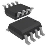
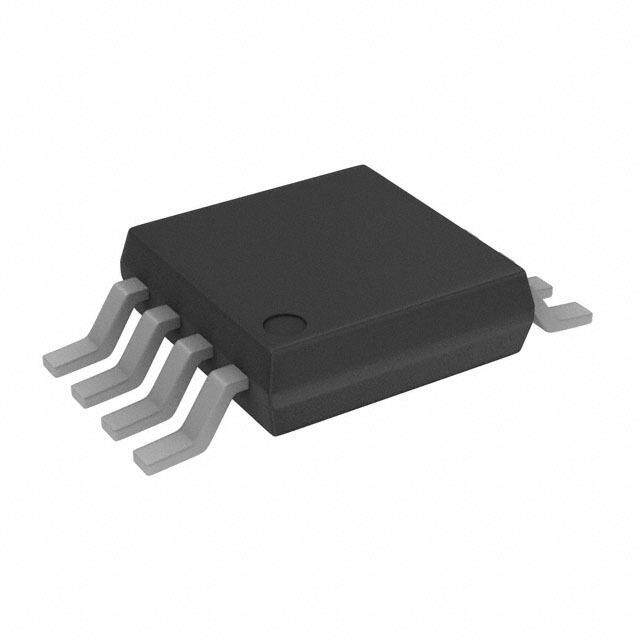
| 产品图片 |
|
| 产品型号 | AD8039SRZ-EPR7 |
| rohs | 无铅 / 符合限制有害物质指令(RoHS)规范要求 |
| 产品系列 | - |
| 供应商器件封装 | 8-SOIC |
| 其它名称 | AD8039SRZ-EPR7DKR |
| 包装 | Digi-Reel® |
| 压摆率 | 425 V/µs |
| 增益带宽积 | - |
| 安装类型 | 表面贴装 |
| 封装/外壳 | 8-SOIC(0.154",3.90mm 宽) |
| 工作温度 | -40°C ~ 85°C |
| 放大器类型 | 电压反馈 |
| 标准包装 | 1 |
| 电压-电源,单/双 (±) | 3 V ~ 12 V, ±1.5 V ~ 6 V |
| 电压-输入失调 | 500µV |
| 电流-电源 | 1mA |
| 电流-输入偏置 | 400pA |
| 电流-输出/通道 | - |
| 电路数 | 2 |
| 输出类型 | - |


- 商务部:美国ITC正式对集成电路等产品启动337调查
- 曝三星4nm工艺存在良率问题 高通将骁龙8 Gen1或转产台积电
- 太阳诱电将投资9.5亿元在常州建新厂生产MLCC 预计2023年完工
- 英特尔发布欧洲新工厂建设计划 深化IDM 2.0 战略
- 台积电先进制程称霸业界 有大客户加持明年业绩稳了
- 达到5530亿美元!SIA预计今年全球半导体销售额将创下新高
- 英特尔拟将自动驾驶子公司Mobileye上市 估值或超500亿美元
- 三星加码芯片和SET,合并消费电子和移动部门,撤换高东真等 CEO
- 三星电子宣布重大人事变动 还合并消费电子和移动部门
- 海关总署:前11个月进口集成电路产品价值2.52万亿元 增长14.8%


PDF Datasheet 数据手册内容提取
Low Power, 350 MHz Voltage Feedback Amplifier AD8039-EP FEATURES FUNCTIONAL BLOCK DIAGRAM Low power: 1 mA quiescent current per amplifier AD8039-EP High speed VOUT1 1 8 +VS −3 dB bandwidth (G = +1): 350 MHz –IN1 2 7 VOUT2 Slew rate: 425 V/μs +IN1 3 6 –IN2 LLooww ncoosist e –VS 4 5 +IN2 09557-001 8 nV/√Hz at 100 kHz Figure 1. 8-Lead SOIC_N 600 fA/√Hz at 100 kHz Low input bias current: 750 nA maximum 24 Low distortion 21 G = +10 −90 dB SFDR at 1 MHz 18 −65 dB SFDR at 5 MHz Wide supply range: 3 V to 12 V 15 G = +5 Small packaging: 8-lead SOIC 12 B) Supports defense and aerospace applications (AQEC standard) d N ( 9 Extended temperature range: −55°C to +105°C AI G = +2 G 6 Controlled manufacturing baseline 3 One assembly/test site G = +1 One fabrication site 0 Enhanced product change notification –3 Qualification data available on request APPLICATIONS –60.1 1 FREQUEN10CY (MHz) 100 100009557-002 Figure 2. Small Signal Frequency Response for Various Gains, Battery-powered instrumentation VOUT = 500 mV p-p, VS = ±5 V Filters ADC drivers Level shifting Buffering Photo multipliers GENERAL DESCRIPTION The AD8039-EP dual amplifier is a high speed (350 MHz) voltage The AD8039-EP amplifier has a wide input common-mode range feedback amplifier with an exceptionally low quiescent current of 1 V from either rail and swings to within 1 V of each rail on the of 1.0 mA per amplifier typical (1.5 mA maximum). Despite its output. This amplifier is optimized for driving capacitive loads up low power and low cost, the amplifier provides excellent overall to 20 pF. If driving larger capacitive loads, a small series resistor performance. Additionally, it offers a high slew rate of 425 V/μs is needed to avoid excessive peaking or overshoot. and a low input offset voltage of 3 mV maximum. The AD8039-EP amplifier is available in an 8-lead SOIC package The Analog Devices, Inc., proprietary XFCB process allows low and is rated to work over the extended temperature range of noise operation (8 nV/√Hz and 600 fA/√Hz) at extremely low −55°C to +105°C. quiescent currents. Given its wide supply voltage range (3 V to Additional application and technical information can be found in 12 V), wide bandwidth, and small packaging, the AD8039-EP the AD8038/AD8039 data sheet. amplifier is designed to work in a variety of applications where power and space are at a premium. Rev. 0 Information furnished by Analog Devices is believed to be accurate and reliable. However, no responsibility is assumed by Analog Devices for its use, nor for any infringements of patents or other One Technology Way, P.O. Box 9106, Norwood, MA 02062-9106, U.S.A. rights of third parties that may result from its use. Specifications subject to change without notice. No license is granted by implication or otherwise under any patent or patent rights of Analog Devices. Tel: 781.329.4700 www.analog.com Trademarks and registered trademarks are the property of their respective owners. Fax: 781.461.3113 ©2011 Analog Devices, Inc. All rights reserved.
AD8039-EP TABLE OF CONTENTS Features .............................................................................................. 1 Absolute Maximum Ratings ............................................................5 Applications ....................................................................................... 1 Maximum Power Dissipation ......................................................5 Functional Block Diagram .............................................................. 1 Output Short Circuit .....................................................................5 General Description ......................................................................... 1 ESD Caution...................................................................................5 Revision History ............................................................................... 2 Typical Performance Characteristics ..............................................6 Specifications ..................................................................................... 3 Outline Dimensions ..........................................................................7 Ordering Guide .............................................................................7 REVISION HISTORY 2/11—Revision 0: Initial Version Rev. 0 | Page 2 of 8
AD8039-EP SPECIFICATIONS T = 25°C, V = ±5 V, R = 2 kΩ, gain = +1, unless otherwise noted. A S L Table 1. Parameter Test Conditions/Comments Min Typ Max Unit DYNAMIC PERFORMANCE −3 dB Bandwidth G = +1, V = 0.5 V p-p, T to T 300 350 MHz OUT MIN MAX G = +2, V = 0.5 V p-p 175 MHz OUT G = +1, V = 2 V p-p 100 MHz OUT Bandwidth for 0.1 dB Flatness G = +2, V = 0.2 V p-p 45 MHz OUT Slew Rate G = +1, V = 2 V step, R = 2 kΩ 400 425 V/μs OUT L T to T 300 325 V/μs MIN MAX Overdrive Recovery Time G = +2, 1 V overdrive 50 ns Settling Time to 0.1% G = +2, V = 2 V step 18 ns OUT NOISE/HARMONIC PERFORMANCE SFDR Second Harmonic f = 1 MHz, V = 2 V p-p, R = 2 kΩ −90 dBc C OUT L Third Harmonic f = 1 MHz, V = 2 V p-p, R = 2 kΩ −92 dBc C OUT L Second Harmonic f = 5 MHz, V = 2 V p-p, R = 2 kΩ −65 dBc C OUT L Third Harmonic f = 5 MHz, V = 2 V p-p, R = 2 kΩ −70 dBc C OUT L Crosstalk, Output-to-Output f = 5 MHz, G = +2 −70 dB Input Voltage Noise f = 100 kHz 8 nV/√Hz Input Current Noise f = 100 kHz 600 fA/√Hz DC PERFORMANCE Input Offset Voltage T = 25°C 0.5 3 mV A T to T 4.5 mV MIN MAX Input Offset Voltage Drift 4.5 μV/°C Input Bias Current T = 25°C 400 750 nA A T to T 2.0 μA MIN MAX Input Bias Current Drift 3 nA/°C Input Offset Current ±25 nA Open-Loop Gain V = ±2.5 V 70 dB OUT INPUT CHARACTERISTICS Input Resistance 10 MΩ Input Capacitance 2 pF Input Common-Mode Voltage Range R = 1 kΩ ±4 V L Common-Mode Rejection Ratio V = ±2.5 V, T = 25°C 61 67 dB CM A V = ±2.5 V, T to T 59 dB CM MIN MAX OUTPUT CHARACTERISTICS DC Output Voltage Swing R = 2 kΩ, saturated output ±4 V L Capacitive Load Drive 30% overshoot, G = +2 20 pF POWER SUPPLY Operating Range 3 12 V Quiescent Current per Amplifier T = 25°C 1.0 1.5 mA A T to T 2.6 mA MIN MAX Power Supply Rejection Ratio −Supply T = 25°C 71 77 dB A T to T 63 dB MIN MAX +Supply T = 25°C 64 70 dB A T to T 63 dB MIN MAX Rev. 0 | Page 3 of 8
AD8039-EP T = 25°C, V = 5 V, R = 2 kΩ to V/2, gain = +1, unless otherwise noted. A S L S Table 2. Parameter Test Conditions/Comments Min Typ Max Unit DYNAMIC PERFORMANCE −3 dB Bandwidth G = +1, V = 0.2 V p-p, T to T 275 300 MHz OUT MIN MAX G = +2, V = 0.2 V p-p 150 MHz OUT G = +1, V = 2 V p-p 30 MHz OUT Bandwidth for 0.1 dB Flatness G = +2, V = 0.2 V p-p 45 MHz OUT Slew Rate G = +1, V = 2 V step, R = 2 kΩ 340 365 V/μs OUT L T to T 275 305 V/μs MIN MAX Overdrive Recovery Time G = +2, 1 V overdrive 50 ns Settling Time to 0.1% G = +2, V = 2 V step 18 ns OUT NOISE/HARMONIC PERFORMANCE SFDR Second Harmonic f = 1 MHz, V = 2 V p-p, R = 2 kΩ −82 dBc C OUT L Third Harmonic f = 1 MHz, V = 2 V p-p, R = 2 kΩ −79 dBc C OUT L Second Harmonic f = 5 MHz, V = 2 V p-p, R = 2 kΩ −60 dBc C OUT L Third Harmonic f = 5 MHz, V = 2 V p-p, R = 2 kΩ −67 dBc C OUT L Crosstalk, Output-to-Output f = 5 MHz, G = +2 −70 dB Input Voltage Noise f = 100 kHz 8 nV/√Hz Input Current Noise f = 100 kHz 600 fA/√Hz DC PERFORMANCE Input Offset Voltage T = 25°C 0.8 3 mV A T to T 4.5 mV MIN MAX Input Offset Voltage Drift 3 μV/°C Input Bias Current T = 25°C 400 750 nA A T to T 2.0 μA MIN MAX Input Bias Current Drift 3 nA/°C Input Offset Current ±30 nA Open-Loop Gain V = ±2.5 V 70 dB OUT INPUT CHARACTERISTICS Input Resistance 10 MΩ Input Capacitance 2 pF Input Common-Mode Voltage Range R = 1 kΩ 1.0 to 4.0 V L Common-Mode Rejection Ratio V = ±1 V, T = 25°C 59 65 dB CM A V = ±1 V, T to T 59 dB CM MIN MAX OUTPUT CHARACTERISTICS DC Output Voltage Swing R = 2 kΩ, saturated output 0.9 to 4.1 V L Capacitive Load Drive 30% overshoot, G = +2 20 pF POWER SUPPLY Operating Range 3 12 V Quiescent Current per Amplifier T = 25°C 0.9 1.5 mA A Power Supply Rejection Ratio T to T 65 71 dB MIN MAX Rev. 0 | Page 4 of 8
AD8039-EP ABSOLUTE MAXIMUM RATINGS 2.0 Table 3. Parameter Rating W) Supply Voltage 12.6 V ON ( 1.5 Power Dissipation See Figure 3 ATI 8-LEAD P SOIC_N Common-Mode Input Voltage ±V SI S S DI Differential Input Voltage ±4 V R 1.0 E Storage Temperature Range −65°C to +125°C W O Operating Temperature Range −55°C to +105°C M P U Lead Temperature (Soldering, 10 sec) 300°C M 0.5 XI A M Stresses above those listed under Absolute Maximum Ratings mrataiyn gca ounsley p; feurmncatnioennat ld oapmeraagteio tno othf et hdee vdiecvei.c Te haits t ihse as es torre sasn y 0–55 –25 AM5BIENT TE3M5PERATU6R5E(°C) 95 125 09557-003 other conditions above those indicated in the operational Figure 3. Maximum Power Dissipation vs. Temperature for a 4-Layer Board section of this specification is not implied. Exposure to absolute RMS output voltages should be considered. If R is referenced to L maximum rating conditions for extended periods may affect −V, as in single-supply operation, then the total drive power is S device reliability. V × I . If the rms signal levels are indeterminate, consider the S OUT MAXIMUM POWER DISSIPATION worst case, when VOUT = VS/4 for RL to midsupply. The maximum safe power dissipation in the AD8039-EP PD = (VS × IS) + (VS/4)2/RL package is limited by the associated rise in junction temperature In single-supply operation with R referenced to −V, worst case L S (TJ) on the die. The plastic encapsulating the die locally reaches is VOUT = VS/2. the junction temperature. At approximately 150°C, which is the Airflow increases heat dissipation, effectively reducing θ . glass transition temperature, the plastic changes its properties. JA In addition, more metal directly in contact with the package Even temporarily exceeding this temperature limit may change leads from metal traces, throughholes, ground, and power the stresses that the package exerts on the die, permanently planes reduces θ . shifting the parametric performance of the AD8039-EP. JA Exceeding a junction temperature of 175°C for an extended Figure 3 shows the maximum safe power dissipation in the time can result in changes in the silicon devices, potentially package vs. the ambient temperature for the 8-lead SOIC_N causing failure. (125°C/W) on a JEDEC standard 4-layer board. θJA values are approximations. The still-air thermal properties of the package and PCB (θ ), JA ambient temperature (T ), and total power dissipated in the OUTPUT SHORT CIRCUIT A package (PD) determine the junction temperature of the die. Shorting the output to ground or drawing excessive current The junction temperature can be calculated as from the AD8039-EP will likely cause a catastrophic failure. TJ = TA + (PD × θJA) The power dissipated in the package (PD) is the sum of the quies- ESD CAUTION cent power dissipation and the power dissipated in the package due to the load drive for all outputs. The quiescent power is the voltage between the supply pins (V) multiplied by the quiescent S current (I). Assuming the load (R) is referenced to midsupply, S L the total drive power is VS/2 × IOUT, some of which is dissipated in the package and some in the load (V × I ). The difference OUT OUT between the total drive power and the load power is the drive power dissipated in the package. P = quiescent power + (total drive power − load power) D P = [V × I] + [(V/2) × (V /R)] − [V 2/R] D S S S OUT L OUT L Rev. 0 | Page 5 of 8
AD8039-EP TYPICAL PERFORMANCE CHARACTERISTICS V = ±5 V, C = 5 pF, R = R = 1 kΩ, R = 2 kΩ, frequency = 1 MHz, T = −55°C to +105°C, unless otherwise noted. S L G F L A 2.0 12 1.5 9 1.0 –40°C 0.5 –55°C 6 B) 0 B) –55°C d d +25°C N (–0.5 +25°C N ( 3 AI AI G–1.0 +105°C +85°C G +105°C 0 –1.5 –2.0 –3 –2.5 –3.0 –6 0.1 1 FREQUE1N0CY (MHz) 100 1000 09557-004 0.1 1 FREQUE1N0CY (MHz) 100 1000 09557-005 Figure 4. Small Signal Frequency Response vs. Temperature, Figure 5. Large Signal Frequency Response vs. Temperature, Gain = +1, VS = ±5 V, VOUT = 500 mV p-p Gain = +2, VS = ±5 V, VOUT = 2 V p-p Rev. 0 | Page 6 of 8
AD8039-EP OUTLINE DIMENSIONS 5.00(0.1968) 4.80(0.1890) 8 5 4.00(0.1574) 6.20(0.2441) 3.80(0.1497) 1 4 5.80(0.2284) 1.27(0.0500) 0.50(0.0196) BSC 1.75(0.0688) 0.25(0.0099) 45° 0.25(0.0098) 1.35(0.0532) 8° 0.10(0.0040) 0° COPLANARITY 0.51(0.0201) 0.10 SEATING 0.31(0.0122) 0.25(0.0098) 10..2470((00..00510507)) PLANE 0.17(0.0067) COMPLIANTTOJEDECSTANDARDSMS-012-AA C(RINOEFNPEATRRREOENNLCLTEIHNEOGSNDELISYM)AEANNRDSEIOARRNOESUNANORDETEDAIN-POMPFRIFLOLMPIMIRLELIATIMTEEERTFSEO;RIRNECUQHSUEDIVIINMAELDENENSSTIIOGSNNFS.OR 012407-A Figure 6. 8-Lead Standard Small Outline Package [SOIC_N] Narrow Body (R-8) Dimensions shown in millimeters and (inches) ORDERING GUIDE Model1 Temperature Range Package Description Package Option AD8039SRZ-EPR7 −55°C to +105°C 8-Lead Standard Small Outline Package [SOIC_N] R-8 1 Z = RoHS Compliant Part. Rev. 0 | Page 7 of 8
AD8039-EP NOTES ©2011 Analog Devices, Inc. All rights reserved. Trademarks and registered trademarks are the property of their respective owners. D09557-0-2/11(0) Rev. 0 | Page 8 of 8