ICGOO在线商城 > 集成电路(IC) > 数据采集 - 模数转换器 > AD7988-1BRMZ
 Datasheet下载
- 型号: AD7988-1BRMZ
- 制造商: Analog
- 库位|库存: xxxx|xxxx
- 要求:
| 数量阶梯 | 香港交货 | 国内含税 |
| +xxxx | $xxxx | ¥xxxx |
查看当月历史价格
查看今年历史价格
AD7988-1BRMZ产品简介:
ICGOO电子元器件商城为您提供AD7988-1BRMZ由Analog设计生产,在icgoo商城现货销售,并且可以通过原厂、代理商等渠道进行代购。 AD7988-1BRMZ价格参考。AnalogAD7988-1BRMZ封装/规格:数据采集 - 模数转换器, 16 Bit Analog to Digital Converter 1 Input 1 SAR 10-MSOP。您可以下载AD7988-1BRMZ参考资料、Datasheet数据手册功能说明书,资料中有AD7988-1BRMZ 详细功能的应用电路图电压和使用方法及教程。
AD7988-1BRMZ是Analog Devices Inc.(亚德诺半导体)生产的一款16位、低功耗、逐次逼近寄存器(SAR)模数转换器(ADC)。它具有高分辨率和快速采样率,适用于多种数据采集应用场景。以下是该型号的主要应用场景:

 1. 工业自动化与控制
AD7988-1BRMZ在工业自动化系统中广泛应用,尤其是在需要高精度测量的场合。例如,它可以用于温度、压力、流量等传感器信号的数字化处理,帮助实现精确的过程监控和控制。其低功耗特性使其适合长时间运行的工业设备,减少了能源消耗。

 2. 医疗设备
在医疗领域,AD7988-1BRMZ可用于各种诊断和监测设备,如心电图(ECG)、血压计、血糖仪等。这些设备需要高精度的模拟信号转换为数字信号,以确保测量结果的准确性。AD7988-1BRMZ的高分辨率和快速响应时间能够满足这些要求,同时其小尺寸设计便于集成到便携式医疗设备中。

 3. 测试与测量仪器
该ADC广泛应用于测试与测量仪器,如示波器、频谱分析仪等。这些仪器需要对输入信号进行精确的数字化处理,以便后续的数据分析和显示。AD7988-1BRMZ的高精度和稳定性使得它成为这些应用的理想选择,特别是在需要高频信号采集的情况下。

 4. 环境监测
环境监测系统通常需要对空气、水质、土壤等多种参数进行实时监测。AD7988-1BRMZ可以用于将传感器采集到的模拟信号转换为数字信号,以便进一步处理和存储。其低功耗和高精度特性非常适合长期部署在户外或偏远地区的监测站。

 5. 汽车电子
在汽车电子系统中,AD7988-1BRMZ可用于车载传感器的数据采集,如发动机温度、油压、胎压等。它能够提供高精度的测量结果,帮助提高车辆的安全性和性能。此外,其紧凑的设计也便于集成到复杂的汽车电子系统中。

总之,AD7988-1BRMZ凭借其高精度、低功耗和快速响应等特点,在多个领域有着广泛的应用前景,特别适合那些对数据采集精度和可靠性要求较高的场景。
| 参数 | 数值 |
| 产品目录 | 集成电路 (IC)半导体 |
| 描述 | ADC 16BIT 100KSPS 1.25LSB 10MSOP模数转换器 - ADC 16-Bit 100ksps Ultra Lo Pwr SAR |
| DevelopmentKit | EVAL-CN0255-SDPZ |
| 产品分类 | |
| 品牌 | Analog Devices |
| 产品手册 | |
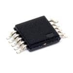
| 产品图片 |
|
| rohs | 符合RoHS无铅 / 符合限制有害物质指令(RoHS)规范要求 |
| 产品系列 | 数据转换器IC,模数转换器 - ADC,Analog Devices AD7988-1BRMZPulSAR® |
| 数据手册 | |
| 产品型号 | AD7988-1BRMZ |
| 产品种类 | 模数转换器 - ADC |
| 位数 | 16 |
| 供应商器件封装 | 10-MSOP |
| 信噪比 | 91 dB |
| 其它名称 | AD79881BRMZ |
| 分辨率 | 16 bit |
| 包装 | 管件 |
| 商标 | Analog Devices |
| 安装类型 | 表面贴装 |
| 安装风格 | SMD/SMT |
| 封装 | Tube |
| 封装/外壳 | 10-TFSOP,10-MSOP(0.118",3.00mm 宽) |
| 封装/箱体 | MSOP-10 |
| 工作温度 | -40°C ~ 125°C |
| 工作电源电压 | 2.5 V |
| 工厂包装数量 | 50 |
| 接口类型 | Serial (3-Wire, 4-Wire, SPI, QSPI, Microwire) |
| 数据接口 | DSP,MICROWIRE™,QSPI™,串行,SPI™ |
| 最大功率耗散 | 0.7 mW |
| 最大工作温度 | + 125 C |
| 最小工作温度 | - 40 C |
| 标准包装 | 50 |
| 特性 | - |
| 电压参考 | External |
| 电压源 | 模拟和数字 |
| 系列 | AD7988-1 |
| 结构 | SAR |
| 转换器数 | 1 |
| 转换器数量 | 1 |
| 转换速率 | 100 kS/s |
| 输入数和类型 | 1 个伪差分,单极 |
| 输入类型 | Differential |
| 通道数量 | 1 Channel |
| 采样率(每秒) | 100k |


PDF Datasheet 数据手册内容提取
16-Bit Lower Power PulSAR ADCs in MSOP/LFCSP Data Sheet AD7988-1/AD7988-5 FEATURES GENERAL DESCRIPTION Low power dissipation The AD7988-1/AD7988-51 are 16-bit, successive approximation, AD7988-1 analog-to-digital converters (ADC) that operate from a single 400 µW at 100 kSPS (VDD only) power supply, VDD. The AD7988-1 offers a 100 kSPS throughput, 700 µW at 100 kSPS (total) and the AD7988-5 offers a 500 kSPS throughput. They are low AD7988-5 power, 16-bit sampling ADCs with a versatile serial interface 2 mW at 500 kSPS (VDD only) port. On the CNV rising edge, they sample an analog input, 3.5 mW at 500 kSPS (total) IN+, between 0 V to V with respect to a ground sense, IN−. REF 16-bit resolution with no missing codes The reference voltage, REF, is applied externally and can be set Throughput: 100 kSPS/500 kSPS options independent of the supply voltage, VDD. INL: ±0.6 LSB typical, ±1.25 LSB maximum The SPI-compatible serial interface also features the ability to SINAD: 91.5 dB at 10 kHz daisy-chain several ADCs on a single 3-wire bus using the SDI THD: −114 dB at 10 kHz input. It is compatible with 1.8 V, 2.5 V, 3 V, or 5 V logic using Pseudo differential analog input range the separate supply, VIO. 0 V to V with V from 2.5 V to 5.0 V REF REF No pipeline delay The AD7988-1/AD7988-5 generics are housed in a 10-lead Single-supply 2.5 V operation with 1.8 V/2.5 V/3 V/5 V logic MSOP or a 10-lead LFCSP with operation specified from −40°C interface to +125°C. Proprietary SPI-/QSPI™-/MICROWIRE™-/DSP-compatible Table 1. MSOP, LFCSP, LGA 14-/16-/18-/20-Bit Precision serial interface SAR ADCs and Integrated SAR ADC μModules® Daisy-chain multiple ADCs μModule 10-lead MSOP and 10-lead, 3 mm × 3 mm LFCSP, same space 400 kSPS Data as SOT-23 to Acquisition Wide operating temperature range: −40°C to +125°C Bits 100 kSPS 250 kSPS 500 kSPS ≥1000 kSPS System 201 AD40202 APPLICATIONS 181 AD7989-12 AD76912 AD40112 AD40032 Battery-powered equipment AD76902 AD40072 Low power data acquisition systems AD7989-52 AD79822 Portable medical instruments AD79842 ATE equipment 161 AD7684 AD76872 AD76882 AD40012 Data acquisitions AD76932 AD40052 AD79162 AD79152 Communications 163 AD7680 AD76852 AD76862 AD40002 ADAQ7980 AD7683 AD7694 AD7988-52 AD40042 ADAQ7988 AD7988-12 AD40082 AD79802 AD79832 143 AD7940 AD79422 AD79462 1 True differential. 2 Pin-for-pin compatible. 3 Pseudo differential. 1 Protected by U.S. Patent 6,703,961. Rev. G Document Feedback Information furnished by Analog Devices is believed to be accurate and reliable. However, no responsibility is assumed by Analog Devices for its use, nor for any infringements of patents or other One Technology Way, P.O. Box 9106, Norwood, MA 02062-9106, U.S.A. rights of third parties that may result from its use. Specifications subject to change without notice. No license is granted by implication or otherwise under any patent or patent rights of Analog Devices. Tel: 781.329.4700 ©2012–2017 Analog Devices, Inc. All rights reserved. Trademarks and registered trademarks are the property of their respective owners. Technical Support www.analog.com
AD7988-1/AD7988-5 Data Sheet TABLE OF CONTENTS Features .............................................................................................. 1 Typical Connection Diagram ................................................... 16 Applications ....................................................................................... 1 Analog Inputs ............................................................................. 17 General Description ......................................................................... 1 Driver Amplifier Choice ........................................................... 17 Revision History ............................................................................... 2 Voltage Reference Input ............................................................ 18 Typical Application Circuit ............................................................. 3 Power Supply ............................................................................... 18 Specifications ..................................................................................... 4 Digital Interface .......................................................................... 18 Timing Specifications .................................................................. 6 CS Mode, 3-Wire ........................................................................ 19 Absolute Maximum Ratings ............................................................ 8 CS Mode 4-Wire ......................................................................... 20 ESD Caution .................................................................................. 8 Chain Mode ................................................................................ 21 Pin Configurations and Function Descriptions ........................... 9 Applications Information .............................................................. 22 Terminology .................................................................................... 10 Interfacing to Blackfin® DSP ..................................................... 22 Typical Performance Characteristics ........................................... 11 Layout .......................................................................................... 22 Theory of Operation ...................................................................... 15 Evaluating the Performance of the AD7988-1/AD7988-5 ..... 22 Circuit Information .................................................................... 15 Outline Dimensions ....................................................................... 23 Converter Operation .................................................................. 15 Ordering Guide .......................................................................... 24 REVISION HISTORY 10/2017—Rev. F to Rev. G Changes to Table 1 ............................................................................. 1 Changes to Features Section and Table 1 ...................................... 1 Changes to AC Accuracy Parameter, Table 2 ................................ 3 Moved Typical Application Circuit Section and Figure 1 ........... 3 Changed nA to μA, Standby Current Parameter, Unit Column, Changes to Figure 5 .......................................................................... 9 Table 3 ................................................................................................. 4 Updated Outline Dimensions ....................................................... 23 Changes to Table 8 .......................................................................... 16 Changes to Ordering Guide .......................................................... 24 Changes to Power Supply Section ................................................ 17 Updated Outline Dimensions ....................................................... 22 4/2016—Rev. E to Rev. F Changed AD7988-x to AD7988-1/AD7988-5 ........... Throughout 8/2013—Rev. C to Rev. D Changes to Table 1 ............................................................................ 1 Changes to Features Section ............................................................ 1 Changes to Table 2 ............................................................................ 3 Changes to Table 3 ............................................................................. 4 Changes to Table 3 ............................................................................ 4 Updated Outline Dimensions ....................................................... 22 Changes to Table 4 ............................................................................ 5 Changes to Ordering Guide .......................................................... 23 Added Table 5: Renumbered Sequentially .................................... 6 Changes to Figure 29 ...................................................................... 14 8/2012—Rev. B to Rev. C Changes to Table 9 .......................................................................... 16 Changes to Ordering Guide .......................................................... 23 Changes to Voltage Reference Input Section .............................. 17 Changes to Figure 35 ...................................................................... 18 5/2012—Rev. A to Rev. B Changes to Figure 37 ...................................................................... 20 Changes to Table 3 ............................................................................. 4 Changes to Ordering Guide .......................................................... 23 Updated Outline Dimensions ....................................................... 22 8/2014—Rev. D to Rev. E 2/2012—Rev. 0 to Rev. A Deleted QFN .................................................................. Throughout Added LFCSP Thermal Impedance Values .................................... 7 Changed Typical Application Diagram Section to Typical Updated Outline Dimensions ....................................................... 23 Application Circuit Section ............................................................. 1 Changes to Ordering Guide .......................................................... 23 Changes to Features Section............................................................ 1 Added Patent Note, Note 1 .............................................................. 1 2/2012—Revision 0: Initial Version Rev. G | Page 2 of 24
Data Sheet AD7988-1/AD7988-5 TYPICAL APPLICATION CIRCUIT 2.5VTO 5V 2.5V REF VDD VIO 1.8VTO 5.5V 0VTO VREF SDI IN+AD7988-1/ AD7988-5 SCK 3- OR 4-WIRE INTERFACE IN– SDO (SPI, DAISY CHAIN, CS) GND CNV 10231-001 Figure 1. Rev. G | Page 3 of 24
AD7988-1/AD7988-5 Data Sheet SPECIFICATIONS VDD = 2.5 V, VIO = 1.71 V to 5.5 V, V = 5 V, T = –40°C to +125°C, unless otherwise noted. REF A Table 2. Parameter Test Conditions/Comments Min Typ Max Unit RESOLUTION 16 Bits ANALOG INPUT Voltage Range IN+ − IN− 0 V V REF Absolute Input Voltage IN+ −0.1 V + 0.1 V REF IN− −0.1 +0.1 V Analog Input CMRR f = 1 kHz 60 dB IN Leakage Current at 25°C Acquisition phase 1 nA Input Impedance See the Analog Inputs section ACCURACY No Missing Codes 16 Bits Differential Linearity Error V = 5 V −0.9 ±0.4 +0.9 LSB1 REF V = 2.5 V ±0.55 LSB1 REF Integral Linearity Error V = 5 V −1.25 ±0.6 +1.25 LSB1 REF V = 2.5 V ±0.65 LSB1 REF Transition Noise V = 5 V 0.6 LSB1 REF V = 2.5 V 1.0 LSB1 REF Gain Error, T to T 2 ±2 LSB1 MIN MAX Gain Error Temperature Drift ±0.35 ppm/°C Zero Error, T to T 2 −0.5 ±0.08 +0.5 mV MIN MAX Zero Temperature Drift 0.54 ppm/°C Power Supply Sensitivity VDD = 2.5 V ± 5% ±0.1 LSB1 THROUGHPUT AD7988-1 Conversion Rate 0 100 kSPS Transient Response Full-scale step 500 ns AD7988-5 Conversion Rate 0 500 kSPS Transient Response Full-scale step 400 ns AC ACCURACY Dynamic Range V = 5 V 92 dB3 REF V = 2.5 V 87 dB3 REF Oversampled Dynamic Range f = 10 kSPS 111 dB3 O Signal-to-Noise Ratio, SNR f = 10 kHz, V = 5 V 90 91.5 dB3 IN REF f = 10 kHz, V = 2.5 V 87 dB3 IN REF Spurious-Free Dynamic Range, SFDR f = 10 kHz −110 dB3 IN Total Harmonic Distortion, THD f = 10 kHz −114 dB3 IN Signal-to-(Noise + Distortion), SINAD f = 10 kHz, V = 5 V 91 dB3 IN REF f = 10 kHz, V = 2.5 V 86.5 dB3 IN REF 1 LSB means least significant bit. With the 5 V input range, 1 LSB is 76.3 µV. 2 See the Terminology section. These specifications include full temperature range variation, but not the error contribution from the external reference. 3 All specifications in dB are referred to a full-scale input FSR. Tested with an input signal at 0.5 dB below full scale, unless otherwise specified. Rev. G | Page 4 of 24
Data Sheet AD7988-1/AD7988-5 VDD = 2.5 V, VIO = 1.71 V to 5.5 V, V = 5 V, T = –40°C to +125°C, unless otherwise noted. REF A Table 3. Parameter Test Conditions/Comments Min Typ Max Unit REFERENCE Voltage Range 2.4 5.1 V Load Current V = 5 V 250 µA REF SAMPLING DYNAMICS −3 dB Input Bandwidth 10 MHz Aperture Delay VDD = 2.5 V 2.0 ns DIGITAL INPUTS Logic Levels V VIO > 3 V –0.3 0.3 × VIO V IL V VIO > 3 V 0.7 × VIO VIO + 0.3 V IH V VIO ≤ 3 V –0.3 0.1 × VIO V IL V VIO ≤ 3 V 0.9 × VIO VIO + 0.3 V IH I −1 +1 µA IL I −1 +1 µA IH DIGITAL OUTPUTS Data Format Serial 16 bits straight binary Pipeline Delay Conversion results available immediately after completed conversion V I = 500 µA 0.4 V OL SINK V I = −500 µA VIO − 0.3 V OH SOURCE POWER SUPPLIES VDD 2.375 2.5 2.625 V VIO 1.71 5.5 V Standby Current1, 2 VDD and VIO = 2.5 V, 25°C 0.35 µA AD7988-1 Power Dissipation VDD = 2.625 V, V = 5 V, VIO = 3 V REF Total 10 kSPS throughput 70 µW 100 kSPS throughput 700 µW 1 mW VDD Only 400 µW REF Only 170 µW VIO Only 130 µW AD7988-5 Power Dissipation VDD = 2.625 V, V = 5 V, VIO = 3 V REF Total 500 kSPS throughput 3.5 5 mW VDD Only 2 mW REF Only 0.85 mW VIO Only 0.65 mW Energy per Conversion 7.0 nJ/sample TEMPERATURE RANGE Specified Performance T to T −40 +125 °C MIN MAX 1 With all digital inputs forced to VIO or GND as required. 2 During the acquisition phase. Rev. G | Page 5 of 24
AD7988-1/AD7988-5 Data Sheet TIMING SPECIFICATIONS VDD = 2.37 V to 2.63 V, VIO = 3.3 V to 5.5 V, −40°C to +125°C unless otherwise stated. See Figure 2 and Figure 3 for load conditions. Table 4. Parameter Symbol Min Typ Max Unit AD7988-1 Throughput Rate 100 kHz Conversion Time: CNV Rising Edge to Data Available t 9.5 μs CONV Acquisition Time t 500 ns ACQ Time Between Conversions t 10 μs CYC AD7988-5 Throughput Rate 500 kHz Conversion Time: CNV Rising Edge to Data Available t CONV B Grade 1.6 µs C Grade 1.2 µs Acquisition Time t ACQ B Grade 400 ns C Grade 800 ns Time Between Conversions t 2 μs CYC CNV Pulse Width (CS Mode) tCNVH 500 ns SCK Period (CS Mode) tSCK VIO Above 4.5 V 10.5 ns VIO Above 3 V 12 ns VIO Above 2.7 V 13 ns VIO Above 2.3 V 15 ns SCK Period (Chain Mode) t SCK VIO Above 4.5 V 11.5 ns VIO Above 3 V 13 ns VIO Above 2.7 V 14 ns VIO Above 2.3 V 16 ns SCK Low Time t 4.5 ns SCKL SCK High Time t 4.5 ns SCKH SCK Falling Edge to Data Remains Valid t 3 ns HSDO SCK Falling Edge to Data Valid Delay t DSDO VIO Above 4.5 V 9.5 ns VIO Above 3 V 11 ns VIO Above 2.7 V 12 ns VIO Above 2.3 V 14 ns CNV or SDI Low to SDO D15 MSB Valid (CS Mode) tEN VIO Above 3 V 10 ns VIO Above 2.3V 15 ns CNV or SDI High or Last SCK Falling Edge to SDO High Impedance (CS Mode) tDIS 20 ns SDI Valid Setup Time from CNV Rising Edge t 5 ns SSDICNV SDI Valid Hold Time from CNV Rising Edge (CS Mode) tHSDICNV 2 ns SDI Valid Hold Time from CNV Rising Edge (Chain Mode) t 0 ns HSDICNV SCK Valid Setup Time from CNV Rising Edge (Chain Mode) t 5 ns SSCKCNV SCK Valid Hold Time from CNV Rising Edge (Chain Mode) t 5 ns HSCKCNV SDI Valid Setup Time from SCK Falling Edge (Chain Mode) t 2 ns SSDISCK SDI Valid Hold Time from SCK Falling Edge (Chain Mode) t 3 ns HSDISCK Rev. G | Page 6 of 24
Data Sheet AD7988-1/AD7988-5 VDD = 2.37 V to 2.63 V, VIO = 1.71 V to 3.3 V, −40°C to +125°C unless otherwise stated. See Figure 2 and Figure 3 for load conditions. Table 5. Parameter Symbol Min Typ Max Unit AD7988-1 Throughput Rate 100 kHz Conversion Time: CNV Rising Edge to Data Available t 9.5 μs CONV Acquisition Time t 500 ns ACQ Time Between Conversions t 10 μs CYC AD7988-5 Throughput Rate 500 kHz Conversion Time: CNV Rising Edge to Data Available t CONV B Grade 1.6 μs C Grade 1.2 μs Acquisition Time t ACQ B Grade 400 ns C Grade 800 ns Time Between Conversions t 2 μs CYC CNV Pulse Width (CS Mode) tCNVH 500 ns SCK Period (CS Mode) tSCK 22 ns SCK Period (Chain Mode) t 23 ns SCK SCK Low Time t 6 ns SCKL SCK High Time t 6 ns SCKH SCK Falling Edge to Data Remains Valid t 3 ns HSDO SCK Falling Edge to Data Valid Delay t 14 21 ns DSDO CNV or SDI Low to SDO D15 MSB Valid (CS Mode) tEN 18 40 ns CNV or SDI High or Last SCK Falling Edge to SDO High Impedance (CS Mode) tDIS 20 ns SDI Valid Setup Time from CNV Rising Edge t 5 ns SSDICNV SDI Valid Hold Time from CNV Rising Edge (CS Mode) tHSDICNV 10 ns SDI Valid Hold Time from CNV Rising Edge (Chain Mode) t 0 ns HSDICNV SCK Valid Setup Time from CNV Rising Edge (Chain Mode) t 5 ns SSCKCNV SCK Valid Hold Time from CNV Rising Edge (Chain Mode) t 5 ns HSCKCNV SDI Valid Setup Time from SCK Falling Edge (Chain Mode) t 2 ns SSDISCK SDI Valid Hold Time from SCK Falling Edge (Chain Mode) t 3 ns HSDISCK 500µA IOL TO SDO 1.4V CL 20pF 500µA IOH 10231-002 Figure 2. Load Circuit for Digital Interface Timing Y% VIO1 X% VIO1 tDELAY tDELAY VIH2 VIH2 VIL2 VIL2 12 FMSOPINREICM VIUIFOMIC ≤ AV 3ITH.I0 OAVNN, SXD I=MN 9A T0XA AIBMNLUDEM Y3 V .=IL 1 U0;S FEODR. S VEIOE D> I3G.0ITVA XL =IN 7P0U, TASND Y = 30. 10231-003 Figure 3. Voltage Levels for Timing Rev. G | Page 7 of 24
AD7988-1/AD7988-5 Data Sheet ABSOLUTE MAXIMUM RATINGS Table 6. Stresses at or above those listed under Absolute Maximum Parameter Rating Ratings may cause permanent damage to the product. This is a Analog Inputs stress rating only; functional operation of the product at these IN+,1 IN−1 to GND −0.3 V to V + 0.3 V or ±130 mA or any other conditions above those indicated in the operational REF Supply Voltage section of this specification is not implied. Operation beyond REF, VIO to GND −0.3 V to +6 V the maximum operating conditions for extended periods may VDD to GND −0.3 V to +3 V affect product reliability. VDD to VIO +3 V to −6 V Digital Inputs to GND −0.3 V to VIO + 0.3 V ESD CAUTION Digital Outputs to GND −0.3 V to VIO + 0.3 V Storage Temperature Range −65°C to +125°C Junction Temperature 150°C θ Thermal Impedance JA 10-Lead MSOP 200°C/W 10-Lead LFCSP 80°C/W θ Thermal Impedance JC 10-Lead MSOP 44°C/W 10-Lead LFCSP 15°C/W Reflow Soldering JEDEC Standard (J-STD-020) 1 See the Analog Inputs section. Rev. G | Page 8 of 24
Data Sheet AD7988-1/AD7988-5 PIN CONFIGURATIONS AND FUNCTION DESCRIPTIONS REF 1 10 VIO VDD 2 AD7988-1/ 9 SDI REF 1 10 VIO IN+ 3 AD7988-5 8 SCK VDD 2 AADD77998888--15/ 9 SDI IN– 4 (NToOt Pto V SIEcWale) 7 SDO IN+ 3 8 SCK GND 5 6 CNV TOPVIEW GINND– 45 (NottoScale) 76 SCDNOV 10231-004 N1.O TTHEES EXPOSEDPAD CAN BE CONNECTEDTO GND. 10231-005 Figure 4. 10-Lead MSOP Pin Configuration Figure 5. 10-Lead LFCSP Pin Configuration Table 7. Pin Function Descriptions Pin No. Mnemonic Type1 Description 1 REF AI Reference Input Voltage. The V range is from 2.4 V to 5.1 V. It is referred to the GND pin. The GND pin REF should be decoupled closely to the REF pin with a 10 μF capacitor. 2 VDD P Power Supply. 3 IN+ AI Analog Input. It is referred to IN−. The voltage range, for example, the difference between IN+ and IN−, is 0 V to V . REF 4 IN− AI Analog Input Ground Sense. Connect to the analog ground plane or to a remote sense ground. 5 GND P Power Supply Ground. 6 CNV DI Convert Input. This input has multiple functions. On its leading edge, it initiates the conversions and selects the interface mode of the part: chain mode or CS mode. In CS mode, the SDO pin is enabled when CNV is low. In chain mode, the data should be read when CNV is high. 7 SDO DO Serial Data Output. The conversion result is output on this pin. It is synchronized to SCK. 8 SCK DI Serial Data Clock Input. When the part is selected, the conversion result is shifted out by this clock. 9 SDI DI Serial Data Input. This input provides multiple features. It selects the interface mode of the ADC as follows: Chain mode is selected if this pin is low during the CNV rising edge. In this mode, SDI is used as a data input to daisy-chain the conversion results of two or more ADCs onto a single SDO line. The digital data level on SDI is output on SDO with a delay of 16 SCK cycles. CS mode is selected if SDI is high during the CNV rising edge. In this mode, either SDI or CNV can enable the serial output signals when low. 10 VIO P Input/Output Interface Digital Power. Nominally at the same supply as the host interface (1.8 V, 2.5 V, 3 V, or 5 V). EP Exposed Pad. The exposed pad can be connected to GND. 1AI = analog input, DI = digital input, DO = digital output, and P = power. Rev. G | Page 9 of 24
AD7988-1/AD7988-5 Data Sheet TERMINOLOGY Effective Resolution Integral Nonlinearity Error (INL) Effective resolution is calculated as INL refers to the deviation of each individual code from a line Effective Resolution = log(2N/RMS Input Noise) drawn from negative full scale through positive full scale. The 2 point used as negative full scale occurs ½ LSB before the first and is expressed in bits. code transition. Positive full scale is defined as a level 1½ LSB Total Harmonic Distortion (THD) beyond the last code transition. The deviation is measured from THD is the ratio of the rms sum of the first five harmonic the middle of each code to the true straight line (see Figure 30). components to the rms value of a full-scale input signal and is Differential Nonlinearity Error (DNL) expressed in dB. In an ideal ADC, code transitions are 1 LSB apart. DNL is the Dynamic Range maximum deviation from this ideal value. It is often specified in Dynamic range is the ratio of the rms value of the full scale to terms of resolution for which no missing codes are guaranteed. the total rms noise measured with the inputs shorted together. The value for dynamic range is expressed in dB. It is measured Offset Error with a signal at −60 dBFS to include all noise sources and DNL The first transition should occur at a level ½ LSB above analog artifacts. ground (38.1 µV for the 0 V to 5 V range). The offset error is the deviation of the actual transition from that point. Signal-to-Noise Ratio (SNR) SNR is the ratio of the rms value of the actual input signal to the Gain Error rms sum of all other spectral components below the Nyquist The last transition (from 111 … 10 to 111 … 11) should frequency, excluding harmonics and dc. The value for SNR is occur for an analog voltage 1½ LSB below the nominal full expressed in dB. scale (4.999886 V for the 0 V to 5 V range). The gain error is the deviation of the actual level of the last transition from the Signal-to-(Noise + Distortion) Ratio (SINAD) ideal level after the offset is adjusted out. SINAD is the ratio of the rms value of the actual input signal to Spurious-Free Dynamic Range (SFDR) the rms sum of all other spectral components below the Nyquist frequency, including harmonics but excluding dc. The value for SFDR is the difference, in decibels (dB), between the rms SINAD is expressed in dB. amplitude of the input signal and the peak spurious signal. Aperture Delay Effective Number of Bits (ENOB) Aperture delay is the measure of the acquisition performance. It ENOB is a measurement of the resolution with a sine wave is the time between the rising edge of the CNV input and when input. It is related to SINAD by the following formula: the input signal is held for a conversion. ENOB = (SINAD − 1.76)/6.02 dB Transient Response and is expressed in bits. Transient response is the time required for the ADC to Noise-Free Code Resolution accurately acquire its input after a full-scale step function is Noise-free code resolution is the number of bits beyond which applied. it is impossible to distinctly resolve individual codes. It is calculated as Noise-Free Code Resolution = log(2N/Peak-to-Peak Noise) 2 and is expressed in bits. Rev. G | Page 10 of 24
Data Sheet AD7988-1/AD7988-5 TYPICAL PERFORMANCE CHARACTERISTICS VDD = 2.5 V, V = 5.0 V, VIO = 3.3 V, unless otherwise noted. REF 0 0 fS = 500kSPS fS = 100kSPS –20 fIN = 10kHz –20 fIN = 10kHz SNR = 91.17dB SNR = 86.7dB E) THD = –113.63dB E) THD = –110.4dB L –40 L –40 A SFDR = 110.30dB A SFDR = 103.9dB C C S SINAD = 91.15dB S SINAD = 86.6dB L –60 L –60 L L U U of F –80 of F –80 B B E (d –100 E (d –100 D D TU –120 TU –120 LI LI P P M –140 M –140 A A –160 –160 –180 –180 0 50 FR10E0QUENCY(1k5H0z) 200 250 10231-046 0 10 FR2E0QUENCY(k3H0z) 40 50 10231-049 Figure 6. AD7988-5 FFT Plot, VREF = 5 V Figure 9. AD7988-1 FFT Plot, VREF = 2.5 V 0 1.25 fS = 500kSPS POSITIVEINL:+0.40LSB –20 fIN = 10kHz 1.00 NEGATIVEINL:–0.35LSB SNR = 86.8dB LE) –40 THD = –111.4dB 0.75 A SFDR = 105.9dB C S SINAD = 86.8dB 0.50 L –60 L B of FU –80 (LSB) 0.205 E (d –100 INL –0.25 D LITU –120 –0.50 P M –140 A –0.75 –160 –1.00 –180 –1.25 0 50 FR10E0QUENCY(1k5H0z) 200 250 10231-047 0 16384 C32O7D68E 49152 65536 10231-010 Figure 7. AD7988-5 FFT Plot, VREF = 2.5 V Figure 10. Integral Nonlinearity vs. Code, VREF = 5 V 0 1.25 fS = 100kSPS POSITIVEINL:+0.45LSB –20 fIN = 10kHz 1.00 NEGATIVEINL:–0.29LSB SNR = 91.09dB LE) –40 THD = –113.12dB 0.75 A SFDR = 110.30dB C S SINAD = 91.05dB 0.50 L –60 L B of FU –80 (LSB) 0.250 E (d –100 INL –0.25 D LITU –120 –0.50 P AM –140 –0.75 –160 –1.00 –180 –1.25 0 10 FR2E0QUENCY(k3H0z) 40 50 10231-048 0 16384 C32O7D68E 49152 65536 10231-011 Figure 8. AD7988-1 FFT Plot, VREF = 5 V Figure 11. Integral Nonlinearity vs. Code, VREF = 2.5 V Rev. G | Page 11 of 24
AD7988-1/AD7988-5 Data Sheet 1.00 60k POSITIVE INL:+0.18LSB NEGATIVEINL:–0.21LSB 50970 0.75 50k 45198 0.50 40k 0.25 B) S S T (L 0 UN 30k DNL CO –0.25 20k 18848 –0.50 12424 10k –0.75 2290 1217 0 0 1 94 30 0 0 –1.00 0 0 16384 C32O7D68E 49152 65536 10231-012 7FFA7FFB7FFC7FFD7FFE7CFOFFDE80 I0N0 H80E0X180028003800480058006 10231-015 Figure 12. Differential Nonlinearity vs. Code, VREF = 5 V Figure 15. Histogram of a DC Input at the Code Transition, VREF = 2.5 V 1.00 100 16 POSITIVE INL:+0.25LSB SNR NEGATIVEINL:–0.22LSB SINAD 0.75 ENOB 0.50 95 15 B) L(LSB) 0.250 SINAD(d 90 14 OB(Bits) DN –0.25 SNR, EN –0.50 85 13 –0.75 –1.00 80 12 0 16384 C32O7D68E 49152 65536 10231-013 2.25 2.75 R3E.2F5ERENCE3.7V5OLTAG4E.2(5V) 4.75 5.25 10231-016 Figure 13. Differential Nonlinearity vs. Code, VREF = 2.5 V Figure 16. SNR, SINAD, and ENOB vs. Reference Voltage 180k 60k 162595 53412 160k 50k 140k 120k 40k COUNTS10800kk COUNTS 30k 37417 31540 60k 52720 20k 42731 40k 10k 7285 20k 5807 0 8000380004820025182009618007C80O08DE80 I0N9 H880E502XA82009B8020C8000D8000E8000F 10231-050 0 7F0FA7F0FB7F1F9C75F9F0D7FFE7CFOFFDE80 I0N0 H80E0X1800285010238101048000580006 10231-051 Figure 14. Histogram of a DC Input at the Code Center, VREF = 5 V Figure 17. Histogram of a DC Input at the Code Center, VREF = 2.5 V Rev. G | Page 12 of 24
Data Sheet AD7988-1/AD7988-5 95 95 94 93 93 92 B) 91 B) 91 d d R( 90 R ( N N S S 89 89 88 87 87 86 85 85 –10 –9 –8INPU–T7LEV–E6L(dB–5OFF–U4LLS–C3ALE)–2 –1 0 10231-018 –55 –35 –15 5TEMP2E5RATU4R5E (°C6)5 85 105 125 10231-053 Figure 18. SNR vs. Input Level Figure 21. SNR vs. Temperature 0.7 –95 115 IVDD 0.6 –100 SFDR 110 0.5 A) –105 105 m THD(dB) –110 100 SFDR(dB) CURRENT ( 00..43 IREF 0.2 –115 THD 95 IVIO 0.1 –120 90 0 –1252.25 2.75 R3E.2F5ERENCE3.7V5OLTAG4E.2(5V) 4.75 5.2585 10231-019 2.375 2.425 V2.D4D75VOLTAG2E.5(2V5) 2.575 2.625 10231-023 Figure 19. THD, SFDR vs. Reference Voltage Figure 22. Operating Currents vs. Supply (AD7988-5) 100 0.14 IVDD 0.12 95 0.10 A) NAD (dB) 90 RRENT (m 00..0068 SI CU IREF 0.04 85 IVIO 0.02 0 8010 FREQUE1N00CY (kHz) 1k 10231-052 2.375 2.425 V2.D4D75VOLTAG2E.5(2V5) 2.575 2.625 10231-024 Figure 20. SINAD vs. Frequency Figure 23. Operating Currents vs. Supply (AD7988-1) Rev. G | Page 13 of 24
AD7988-1/AD7988-5 Data Sheet –85 0.14 IVDD –90 0.12 –95 0.10 –100 A) dB) T (m 008 D (–105 EN H R T R 0.06 –110 CU IREF 0.04 –115 IVIO –120 0.02 –125 0 10 FREQUE1N00CY (kHz) 1k 10231-054 –55 –35 –15 5TEMP2E5RATU4R5E(°C6)5 85 105 125 10231-028 Figure 24. THD vs. Frequency Figure 27. Operating Currents vs. Temperature (AD7988-1) –110 8 7 –112 6 A) 5 D(dB) –114 ENT (µ 4 H R T R –116 U C 3 IVDD + IVIO 2 –118 1 –120 0 –55 –35 –15 5TEMP2E5RATU4R5E(°C6)5 85 105 125 10231-026 –55 –35 –15 5TEMP2E5RATU4R5E (°C6)5 85 105 125 10231-029 Figure 25. THD vs. Temperature Figure 28. Power-Down Currents vs. Temperature 0.7 IVDD 0.6 0.5 A) m T ( 0.4 N E R R 0.3 CU IREF 0.2 IVIO 0.1 0 –55 –35 –15 5TEMP2E5RATU4R5E(°C6)5 85 105 125 10231-027 Figure 26. Operating Currents vs. Temperature (AD7988-5) Rev. G | Page 14 of 24
Data Sheet AD7988-1/AD7988-5 THEORY OF OPERATION IN+ MSB SWITCHES CONTROL LSB SW+ 32,768C 16,384C 4C 2C C C REF COMP CONTROL GND LOGIC OUTPUT CODE 32,768C 16,384C 4C 2C C C LSB SW– MSB CNV IN– 10231-030 Figure 29. ADC Simplified Schematic CIRCUIT INFORMATION During the acquisition phase, terminals of the array tied to the comparator’s input are connected to GND via SW+ and SW−. The AD7988-1/AD7988-5 devices are fast, low power, single- All independent switches are connected to the analog inputs. supply, precise 16-bit ADCs that use a successive approximation Therefore, the capacitor arrays are used as sampling capacitors architecture. and acquire the analog signal on the IN+ and IN− inputs. When The AD7988-1 is capable of converting 100,000 samples per the acquisition phase is completed and the CNV input goes high, a second (100 kSPS), whereas the AD7988-5 is capable of a conversion phase is initiated. When the conversion phase begins, throughput of 500 kSPS, and they power down between SW+ and SW− are opened first. The two capacitor arrays are then conversions. When operating at 10 kSPS, for example, the disconnected from the inputs and connected to the GND input. ADC consumes 70 µW typically, ideal for battery-powered Therefore, the differential voltage between the IN+ and IN− applications. inputs captured at the end of the acquisition phase are applied to the comparator inputs, causing the comparator to become The AD7988-1/AD7988-5 provide the user with on-chip track- unbalanced. By switching each element of the capacitor array and-hold and does not exhibit any pipeline delay or latency, between GND and REF, the comparator input varies by binary making it ideal for multiple multiplexed channel applications. weighted voltage steps (V /2, V /4 … V /65,536). The REF REF REF The AD7988-1/AD7988-5 can be interfaced to any 1.8 V to 5 V control logic toggles these switches, starting with the MSB, to digital logic family. It is housed in a 10-lead MSOP or a tiny 10- bring the comparator back into a balanced condition. After the lead LFCSP that combines space savings and allows flexible completion of this process, the part returns to the acquisition phase configurations. and the control logic generates the ADC output code. CONVERTER OPERATION Because the AD7988-1/AD7988-5 have an on-board conversion The AD7988-1/AD7988-5 are successive approximation ADCs clock, the serial clock, SCK, is not required for the conversion based on a charge redistribution DAC. Figure 29 shows the process. simplified schematic of the ADC. The capacitive DAC consists of two identical arrays of 16 binary weighted capacitors, which are connected to the two comparator inputs. Rev. G | Page 15 of 24
AD7988-1/AD7988-5 Data Sheet Transfer Functions Table 8. Output Codes and Ideal Input Voltages The ideal transfer characteristic for the AD7988-1/AD7988-5 is Analog Input shown in Figure 30 and Table 8. Description VREF = 5 V Digital Output Code (Hex) FSR – 1 LSB 4.999924 V FFFF1 Midscale + 1 LSB 2.500076 V 8001 111 ...111 Midscale 2.5 V 8000 ARY)111111 ...... 111001 Midscale – 1 LSB 2.499924 V 7FFF BIN –FSR + 1 LSB 76.3 µV 0001 HT –FSR 0 V 00002 G AI E (STR 12 TThhiiss iiss aallssoo t thhee c cooddee fo fro ar na no vuenrrdaenrgraendg aenda laonga inlopgu tin (VpINu+t − (V VININ+− −ab VoINv−e b VeRlEoF −w V VGGNNDD).) . D O TYPICAL CONNECTION DIAGRAM C C AD Figure 31 shows an example of the recommended connection 000 ... 010 diagram for the AD7988-1/AD7988-5 when multiple supplies 000 ... 001 are available. 000 ... 000 –FSR –FSR + 1LSB +FSR – 1 LSB –FSR + 0.5LSB ANALOG INP+UFTSR – 1.5 LSB 10231-031 Figure 30. ADC Ideal Transfer Function V+ REF1 2.5V 10µF2 100nF V+ 1.8V TO 5.5V 100nF 20Ω 0V TO VREF REF VDD VIO 3 IN+ SDI 2.7nF V– AADD77998888--15/ SSDCOK 3- OR 4-WIRE INTERFACE5 4 IN– CNV GND 1SEE THE VOLTAGE REFERENCE INPUT SECTION FOR REFERENCE SELECTION. 2CREF IS USUALLY A 10µF CERAMIC CAPACITOR (X5R). 345SOSEEPEET ITTOHHNEEA DLD IRFGIIVILTETARELR AI.N MSTPEELERI FFTIAHECER E AC SNHEAOCLICTOEIGO S NINE FPCOUTRITO STN HS.EE CMTOIOSNT. CONVENIENT INTERFACE MODE. 10231-032 Figure 31. Typical Application Diagram with Multiple Supplies Rev. G | Page 16 of 24
Data Sheet AD7988-1/AD7988-5 ANALOG INPUTS DRIVER AMPLIFIER CHOICE Figure 32 shows an equivalent circuit of the input structure of Although the AD7988-1/AD7988-5 are easy to drive, the driver the AD7988-1/AD7988-5. amplifier needs to meet the following requirements: The two diodes, D1 and D2, provide ESD protection for the • The noise generated by the driver amplifier must be kept as analog inputs, IN+ and IN−. Care must be taken to ensure that low as possible to preserve the SNR and transition noise the analog input signal never exceeds the supply rails by more performance of the AD7988-1/AD7988-5. The noise than 0.3 V, because this causes these diodes to become forward- coming from the driver is filtered by the AD7988-1/ biased and start conducting current. These diodes can handle a AD7988-5 analog input circuit’s one-pole, low-pass filter forward-biased current of 130 mA maximum. For instance, made by R and C or by the external filter, if one is used. IN IN these conditions may eventually occur when the input buffer’s Because the typical noise of the AD7988-1/AD7988-5 is supplies are different from VDD. In such a case (for example, an 47.3 µV rms, the SNR degradation due to the amplifier is input buffer with a short circuit), the current limitation can be used to protect the part. 47.3 REF SNR =20log LOSS π 47.32+ f (Ne )2 D1 RIN CIN 2 −3dB N IN+ OR IN– • where: GND CPIN D2 10231-033 Af–3DdB7 is9 8th8e-5 i n(p1u0t M baHnzd)w oidr tthh ein c MutHofzf ofrfe tqhuee AnDcy7 9o8f 8th-1e/ input Figure 32. Equivalent Analog Input Circuit filter, if one is used. N is the noise gain of the amplifier (for example, 1 in buffer The analog input structure allows the sampling of the true configuration). differential signal between IN+ and IN−. By using these e is the equivalent input noise voltage of the op amp, in differential inputs, signals common to both inputs are rejected. N nV/√Hz. During the acquisition phase, the impedance of the analog • For ac applications, the driver should have a THD inputs (IN+ and IN−) can be modeled as a parallel combination of performance commensurate with the AD7988-1/AD7988-5. Capacitor C and the network formed by the series connection of PIN • For multichannel multiplexed applications, the driver ampli- R and C . C is primarily the pin capacitance. R is typically IN IN PIN IN fier and the AD7988-1/AD7988-5 analog input circuit must 400 Ω and is a lumped component made up of serial resistors settle for a full-scale step onto the capacitor array at a and the on resistance of the switches. C is typically 30 pF and IN 16-bit level (0.0015%, 15 ppm). In the amplifier data sheet, is mainly the ADC sampling capacitor. During the conversion settling at 0.1% to 0.01% is more commonly specified. This phase, when the switches are opened, the input impedance is may differ significantly from the settling time at a 16-bit limited to C . R and C make a one-pole, low-pass filter that PIN IN IN level and should be verified prior to driver selection. reduces undesirable aliasing effects and limits the noise. Table 9. Recommended Driver Amplifiers1 When the source impedance of the driving circuit is low, the Amplifier Typical Application AD7988-1/AD7988-5 can be driven directly. Large source impedances significantly affect the ac performance, especially ADA4805-1 Low noise, small size, and low power THD. The dc performances are less sensitive to the input ADA4807-1 Very low noise and high frequency impedance. The maximum source impedance depends on the ADA4627-1 Precision, low noise, and low input bias amount of THD that can be tolerated. The THD degrades as a ADA4522-1 Precision, zero-drift, and EMI enhanced function of the source impedance and the maximum input ADA4500-2 Precision, RRIO, and zero input crossover distortion frequency. 1 For the latest recommended drivers, see the product recommendations listed on the product webpage. Rev. G | Page 17 of 24
AD7988-1/AD7988-5 Data Sheet VOLTAGE REFERENCE INPUT The AD7988-1/AD7988-5 powers down automatically at the end of each conversion phase. The AD7988-1/AD7988-5 voltage reference input, REF, has a dynamic input impedance and must therefore be driven by a DIGITAL INTERFACE low impedance source with efficient decoupling between the Although the AD7988-1/AD7988-5 have a reduced number of REF and GND pins, as explained in the Layout section. pins, it offers flexibility in its serial interface modes. When REF is driven by a very low impedance source, for example, The AD7988-1/AD7988-5, when in CS mode, is compatible with a reference buffer using the AD8031 or the ADA4805-1, a SPI, QSPI™, and digital hosts. This interface can use either a 3-wire ceramic chip capacitor is appropriate for optimum or 4-wire interface. A 3-wire interface using the CNV, SCK, and performance. SDO signals minimizes wiring connections and is useful, for If an unbuffered reference voltage is used, the decoupling value instance, in isolated applications. A 4-wire interface using the depends on the reference used. For example, a 22 µF (X5R, SDI, CNV, SCK, and SDO signals allows CNV, which initiates 1206 size) ceramic chip capacitor is appropriate for optimum the conversions, to be independent of the readback timing performance using a low temperature drift ADR435 reference. (SDI). This is useful in low jitter sampling or simultaneous If desired, a reference-decoupling capacitor value as small as sampling applications. 2.2 µF can be used with a minimal impact on performance, The AD7988-1/AD7988-5, when in chain mode, provides a especially DNL. daisy-chain feature using the SDI input for cascading multiple Regardless, there is no need for an additional lower value ceramic ADCs on a single data line, similar to a shift register. decoupling capacitor (for example, 100 nF) between the REF The mode in which the part operates depends on the SDI level and GND pins. when the CNV rising edge occurs. CS mode is selected if SDI is POWER SUPPLY high, and chain mode is selected if SDI is low. The SDI hold time is such that when SDI and CNV are connected together, The AD7988-1/AD7988-5 use two power supply pins: a core the chain mode is selected. supply, VDD, and a digital input/output interface supply, VIO. VIO allows direct interface with any logic between 1.8 V and The user must time out the maximum conversion time prior to 5.0 V. To reduce the number of supplies needed, VIO and VDD readback. can be tied together. The AD7988-1/AD7988-5 are independent of power supply sequencing between VIO and VDD. Additionally, it is very insensitive to power supply variations over a wide frequency range, as shown in Figure 33. 80 75 B) 70 d R ( R S P 65 60 55 1 10FREQUENCY (kHz)100 1k 10231-034 Figure 33. PSRR vs. Frequency Rev. G | Page 18 of 24
Data Sheet AD7988-1/AD7988-5 CS MODE, 3-WIRE When CNV goes low, the MSB is output onto SDO. The remaining data bits are then clocked by subsequent SCK falling edges. The This mode is typically used when a single AD7988-1or AD7988-5 data is valid on both SCK edges. Although the rising edge can is connected to an SPI-compatible digital host. The connection be used to capture the data, a digital host using the SCK falling diagram is shown in Figure 34, and the corresponding timing is edge allows a faster reading rate, provided that it has an acceptable given in Figure 35. hold time. After the 16th SCK falling edge or when CNV goes With SDI tied to VIO, a rising edge on CNV initiates a conver- high, whichever is earlier, SDO returns to high impedance. sion, selects the CS mode, and forces SDO to high impedance. When the conversion is complete, the AD7988-1/AD7988-5 enter the acquisition phase and powers down. CONVERT CNV DIGITAL HOST VIO AD7988-1/ SDI AD7988-5 SDO DATA IN SCK CLK 10231-035 Figure 34. 3-Wire CS Mode Connection Diagram SDI = 1 t CYC t CNVH CNV tCONV tACQ ACQUISITION CONVERSION ACQUISITION t SCK t SCKL SCK 1 2 3 14 15 16 tHSDO tSCKH tEN tDSDO tDIS SDO D15 D14 D13 D1 D0 10231-036 Figure 35. 3-Wire CS Mode Serial Interface Timing (SDI High) Rev. G | Page 19 of 24
AD7988-1/AD7988-5 Data Sheet CS MODE 4-WIRE When the conversion is complete, the AD7988-1/AD7988-5 enter the acquisition phase and powers down. Each ADC result This mode is typically used when multiple AD7988-1/AD7988-5 can be read by bringing its SDI input low, which consequently devices are connected to an SPI-compatible digital host. outputs the MSB onto SDO. The remaining data bits are then A connection diagram example using the AD7988-1/AD7988-5 clocked by subsequent SCK falling edges. The data is valid on devices are shown in Figure 36, and the corresponding timing is both SCK edges. Although the rising edge can be used to capture given in Figure 37. the data, a digital host using the SCK falling edge allows a faster With SDI high, a rising edge on CNV initiates a conversion, reading rate, provided that it has an acceptable hold time. After selects the CS mode, and forces SDO to high impedance. In this the 16th SCK falling edge or when SDI goes high, whichever is mode, CNV must be held high during the conversion phase and earlier, SDO returns to high impedance and another AD7988-1 the subsequent data readback (if SDI and CNV are low, SDO is or AD7988-5 can be read. driven low). Prior to the minimum conversion time, SDI can be used to select other SPI devices, such as analog multiplexers, but SDI must be returned high before the minimum conversion time elapses and then held high for the maximum conversion time. CS2 CS1 CONVERT CNV CNV DIGITAL HOST AD7988-1/ AD7988-1/ SDI AD7988-5 SDO SDI AD7988-5 SDO SCK SCK CDLAKTA IN 10231-037 Figure 36. 4-Wire CS Mode Connection Diagram t CYC CNV tCONV tACQ ACQUISITION CONVERSION ACQUISITION t SSDICNV SDI (CS1) t HSDICNV SDI (CS2) t SCK t SCKL SCK 1 2 3 14 15 16 17 18 30 31 32 tHSDO tSCKH tEN tDSDO tDIS SDO D15 D14 D13 D1 D0 D15 D14 D1 D0 10231-038 Figure 37. 4-Wire CS Mode Serial Interface Timing Rev. G | Page 20 of 24
Data Sheet AD7988-1/AD7988-5 CHAIN MODE phase and the subsequent data readback. When the conversion is complete, the MSB is output onto SDO and the AD7988-1/ This mode can be used to daisy-chain multiple AD7988-1/ AD7988-5 enter the acquisition phase and power down. The AD7988-5 devices on a 3-wire serial interface. This feature is remaining data bits stored in the internal shift register are useful for reducing component count and wiring connections, for clocked by subsequent SCK falling edges. For each ADC, SDI example, in isolated multiconverter applications or for systems feeds the input of the internal shift register and is clocked by the with a limited interfacing capacity. Data readback is analogous SCK falling edge. Each ADC in the chain outputs its data MSB to clocking a shift register. first, and 16 × N clocks are required to read back the N ADCs. A connection diagram example using the AD7988-1/AD7988-5 The data is valid on both SCK edges. Although the rising edge devices is shown in Figure 38, and the corresponding timing is can be used to capture the data, a digital host using the SCK given in Figure 39. falling edge allows a faster reading rate and, consequently, more When SDI and CNV are low, SDO is driven low. With SCK low, AD7988-1/ AD7988-5 devices in the chain, provided that the a rising edge on CNV initiates a conversion and selects the chain digital host has an acceptable hold time. The maximum mode. In this mode, CNV is held high during the conversion conversion rate may be reduced due to the total readback time. CONVERT CNV CNV DIGITAL HOST AD7988-1/ AD7988-1/ SDI AD7988-5 SDO SDI AD7988-5 SDO DATA IN A B SCK SCK CLK 10231-039 Figure 38. Chain Mode Connection Diagram SDIA = 0 tCYC CNV tCONV tACQ ACQUISITION CONVERSION ACQUISITION tSCK tSSCKCNV tSCKL SCK 1 2 3 14 15 16 17 18 30 31 32 tHSCKCNV tSSDISCK tSCKH tEN tHSDISCK SDOA = SDIB DA15 DA14 DA13 DA1 DA0 tHSDO tDSDO SDOB DB15 DB14 DB13 DB1 DB0 DA15 DA14 DA1 DA0 10231-040 Figure 39. Chain Mode Serial Interface Timing Rev. G | Page 21 of 24
AD7988-1/AD7988-5 Data Sheet APPLICATIONS INFORMATION INTERFACING TO BLACKFIN® DSP Using at least one ground plane is recommended. It can be common or split between the digital and analog section. In the The AD7988-1/AD7988-5 can easily connect to a DSP SPI or latter case, join the planes underneath the AD7988-1/AD7988-5 SPORT. The SPI configuration is straightforward, using the devices. standard SPI interface as shown in Figure 40. The AD7988-1/AD7988-5 voltage reference input, REF, has a dynamic input impedance. Decouple REF with minimal parasitic SPI_CLK SCK inductances by placing the reference decoupling ceramic capacitor BLACKFIN SPI_MISO SDO AD7988-1/ close to, but ideally right up against, the REF and GND pins and DSP AD7988-5 SPI_MOSI CNV 10231-041 cFoinnanlleyc, tdinegc otuhpemle twhiet hp owwideer ,s luopwp ilmiesp oefd tahnec eA tDra7c9e8s8. -1/AD7988-5, Figure 40. Typical Connection to Blackfin SPI Interface VDD and VIO, with ceramic capacitors, typically 100 nF, placed close to the AD7988-1/AD7988-5 and connected using short and Similarly, the SPORT interface can be used to interface to this wide traces to provide low impedance paths and to reduce the ADC. The SPORT interface has some benefits in that it can use effect of glitches on the power supply lines. direct memory access (DMA) and provides a lower jitter CNV An example of a layout following these rules is shown in Figure 42 signal generated from a hardware counter. and Figure 43. Some glue logic may be required between SPORT and the EVALUATING THE PERFORMANCE OF THE AD7988-1/AD7988-5 interface. The evaluation board for the AD7988-1/AD7988-5 AD7988-1/AD7988-5 interfaces directly to the SPORT of the The evaluation board package for the AD7988-1/AD7988-5 Blackfin-based (ADSP-BF527) SDP board. The configuration (EVAL-AD7988-5SDZ) includes a fully assembled and tested used for the SPORT interface requires the addition of some glue evaluation board, documentation, and software for controlling the logic as shown in Figure 41. The SCK input to the ADC was board from a PC via the EVAL-SDP-CB1Z. gated off when CNV was high to keep the SCK line static while converting the data, thereby ensuring the best integrity of the AD7988-1/ result. This approach uses an AND gate and a NOT gate for the AD7988-5 SCK path. The other logic gates used on the RSCLK and RFS paths are for delay matching purposes and may not be necessary where path lengths are short. This is one approach to using the SPORT interface for this ADC; there may be other solutions equal to this approach. VDRIVE DR SDO RSCLK TSCLK BLADCSKPFIN RFS SCKAADD77998888--15/ 10231-043 Figure 42. Example Layout of the AD7988-1/AD7988-5 (Top Layer) TFS CNV 10231-045 Figure 41. Evaluation Board Connection to Blackfin Sport Interface LAYOUT Design the printed circuit board (PCB) that houses the AD7988-1/ AD7988-5 so that the analog and digital sections are separated and confined to certain areas of the board. The pinout of the AD7988-1/AD7988-5, with all the analog signals on the left side and all the digital signals on the right side, eases this task. Avoid running digital lines under the device because these couple noise onto the die, unless a ground plane under the AD7988-1/ AD7988-5 is used as a shield. Fast switching signals, such as CAvNoVid o crr oclsoscokvse,r s ohfo duilgdi tnael vaenrd r aunna nloega rs iagnnaallosg. signal paths. 10231-044 Figure 43. Example Layout of the AD7988-1/AD7988-5 (Bottom Layer) Rev. G | Page 22 of 24
Data Sheet AD7988-1/AD7988-5 OUTLINE DIMENSIONS 3.10 3.00 2.90 10 6 5.15 3.10 4.90 3.00 4.65 2.90 1 5 PIN1 IDENTIFIER 0.50BSC 0.95 15°MAX 0.85 1.10MAX 0.75 0.70 0.15 0.30 6° 0.23 0.55 CO0P.0L5ANARITY 0.15 0° 0.13 0.40 0.10 COMPLIANTTOJEDECSTANDARDSMO-187-BA 091709-A Figure 44.10-Lead Mini Small Outline Package [MSOP] (RM-10) Dimensions shown in millimeters DETAIL A (JEDEC 95) 2.48 2.38 3.10 2.23 3.00 SQ 2.90 0.50 BSC 6 10 PIN 1 INDEX EXPOSED 1.74 AREA PAD 1.64 0.50 1.49 0.40 0.30 5 1 0.20 MIN TOP VIEW BOTTOM VIEW PININD I1CATOR AREA OPTIONS (SEE DETAIL A) 0.80 FOR PROPER CONNECTION OF 0.75 SIDE VIEW 0.05 MAX THE EXPOSED PAD, REFER TO THE PIN CONFIGURATION AND 0.70 0.02 NOM FUNCTION DESCRIPTIONS COPLANARITY SECTION OF THIS DATA SHEET. PKG-004362 SEPALTAINNGE 000...322050 0.20 REF 0.08 02-07-2017-C Figure 45. 10-Lead Lead Frame Chip Scale Package [LFCSP] 3 mm × 3 mm Body and 0.75 mm Package Height (CP-10-9) Dimensions shown in millimeters Rev. G | Page 23 of 24
AD7988-1/AD7988-5 Data Sheet ORDERING GUIDE Integral Temperature Ordering Package Model1, 2, 3 Nonlinearity Range Quantity Package Description Option Branding AD7988-1BRMZ ±1.25 LSB max −40°C to +125°C Tube, 50 10-Lead MSOP RM-10 C7E AD7988-1BRMZ-RL7 ±1.25 LSB max −40°C to +125°C Reel, 1,000 10-Lead MSOP RM-10 C7E AD7988-1BCPZ-RL ±1.25 LSB max −40°C to +125°C Reel, 5,000 10-Lead LFCSP CP-10-9 C7X AD7988-1BCPZ-RL7 ±1.25 LSB max −40°C to +125°C Reel, 1,500 10-Lead LFCSP CP-10-9 C7X AD7988-5BRMZ ±1.25 LSB max −40°C to +125°C Tube, 50 10-Lead MSOP RM-10 C7Q AD7988-5BRMZ-RL7 ±1.25 LSB max −40°C to +125°C Reel, 1,000 10-Lead MSOP RM-10 C7Q AD7988-5BCPZ-RL ±1.25 LSB max −40°C to +125°C Reel, 5,000 10-Lead LFCSP CP-10-9 C7Z AD7988-5BCPZ-RL7 ±1.25 LSB max −40°C to +125°C Reel, 1,500 10-Lead LFCSP CP-10-9 C7Z AD7988-5CCPZ-RL ±1.25 LSB max −40°C to +125°C Reel, 5,000 10-Lead LFCSP CP-10-9 C8P AD7988-5CCPZ-RL7 ±1.25 LSB max −40°C to +125°C Reel, 1,500 10-Lead LFCSP CP-10-9 C8P EVAL-AD7988-5SDZ Evaluation Board with the AD7988-5 Populated; Use for the Evaluation of both the AD7988-1 and the AD7988-5 EVAL-SDP-CB1Z System Demonstration Board; Used as a Controller Board for Data Transfer via USB Interface to PC 1 Z = RoHS Compliant Part. 2 The EVAL-AD7988-5SDZ can be used as a standalone evaluation board or in conjunction with the EVAL-SDZ-CB1Z for evaluation and/or demonstration purposes. 3 The EVAL-SDP-CB1Z allows a PC to control and communicate with all Analog Devices, Inc., evaluation boards ending in the SD designator. ©2012–2017 Analog Devices, Inc. All rights reserved. Trademarks and registered trademarks are the property of their respective owners. D10231-0-10/17(G) Rev. G | Page 24 of 24
Mouser Electronics Authorized Distributor Click to View Pricing, Inventory, Delivery & Lifecycle Information: A nalog Devices Inc.: AD7988-1BCPZ-RL7 AD7988-1BRMZ AD7988-5BRMZ AD7988-1BRMZ-RL7 AD7988-5BCPZ-RL EVAL-AD7988- 5SDZ AD7988-5BCPZ-RL7 AD7988-5BRMZ-RL7 AD7988-1BCPZ-RL AD7988-5CCPZ-RL7 AD7988-5CCPZ-RL