ICGOO在线商城 > 集成电路(IC) > 数据采集 - 数模转换器 > AD7564BRS
 Datasheet下载
- 型号: AD7564BRS
- 制造商: Analog
- 库位|库存: xxxx|xxxx
- 要求:
| 数量阶梯 | 香港交货 | 国内含税 |
| +xxxx | $xxxx | ¥xxxx |
查看当月历史价格
查看今年历史价格
AD7564BRS产品简介:
ICGOO电子元器件商城为您提供AD7564BRS由Analog设计生产,在icgoo商城现货销售,并且可以通过原厂、代理商等渠道进行代购。 AD7564BRS价格参考。AnalogAD7564BRS封装/规格:数据采集 - 数模转换器, 12 位 数模转换器 4 28-SSOP。您可以下载AD7564BRS参考资料、Datasheet数据手册功能说明书,资料中有AD7564BRS 详细功能的应用电路图电压和使用方法及教程。
AD7564BRS 是由 Analog Devices Inc.(ADI)生产的一款数据采集系统的数模转换器(DAC)。它属于 12 位双极性电压输出 DAC,广泛应用于需要高精度、低功耗和快速建立时间的场景。以下是其主要应用场景:

 1. 工业自动化与控制
   - 在工业控制系统中,AD7564BRS 可用于生成精确的控制信号,驱动执行器或调节阀门。
   - 它适用于可编程逻辑控制器(PLC)、分布式控制系统(DCS)以及运动控制系统中的信号生成。

 2. 测试与测量设备
   - AD7564BRS 的高精度和稳定性使其成为测试仪器(如示波器、信号发生器)的理想选择。
   - 可用于校准系统、精密电源或任意波形发生器中,提供准确的电压输出。

 3. 通信系统
   - 在通信领域,AD7564BRS 可用于基带信号生成,支持数字信号到模拟信号的转换。
   - 其快速建立时间和低噪声特性适合高速数据传输应用。

 4. 医疗设备
   - 在医疗电子领域,AD7564BRS 可用于超声波设备、心电图(ECG)监测仪等需要精确信号生成的场合。
   - 提供稳定的电压输出以驱动传感器或执行器,确保诊断结果的准确性。

 5. 汽车电子
   - 用于汽车控制系统中,例如发动机管理、悬挂控制和制动系统。
   - 提供精确的模拟输出信号,以实现对各种传感器和执行器的控制。

 6. 消费电子产品
   - 在音频处理和视频设备中,AD7564BRS 可用于数字信号到模拟信号的转换,确保高质量的音视频输出。
   - 适用于家用音响设备、游戏机和其他多媒体设备。

 7. 航空航天与国防
   - 在高精度要求的航空航天和国防应用中,AD7564BRS 可用于雷达系统、导航设备和导弹控制系统。
   - 提供稳定可靠的信号生成能力,满足严苛的工作环境需求。

 总结
AD7564BRS 凭借其 12 位分辨率、双极性输出范围(±10V 或 ±5V)以及出色的线性度和低功耗特性,适用于多种需要高精度和可靠性的场景。无论是工业控制还是消费电子,该器件都能为用户提供卓越的性能表现。
| 参数 | 数值 |
| 产品目录 | 集成电路 (IC) |
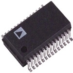
| 描述 | IC DAC 12BIT LC2MOS QUAD 28-SSOP |
| 产品分类 | |
| 品牌 | Analog Devices Inc |
| 数据手册 | |
| 产品图片 |
|
| 产品型号 | AD7564BRS |
| rohs | 不符合限制有害物质指令(RoHS)规范要求 |
| 产品系列 | - |
| 产品培训模块 | http://www.digikey.cn/PTM/IndividualPTM.page?site=cn&lang=zhs&ptm=19145http://www.digikey.cn/PTM/IndividualPTM.page?site=cn&lang=zhs&ptm=18614http://www.digikey.cn/PTM/IndividualPTM.page?site=cn&lang=zhs&ptm=26125http://www.digikey.cn/PTM/IndividualPTM.page?site=cn&lang=zhs&ptm=26140http://www.digikey.cn/PTM/IndividualPTM.page?site=cn&lang=zhs&ptm=26150http://www.digikey.cn/PTM/IndividualPTM.page?site=cn&lang=zhs&ptm=26147 |
| 位数 | 12 |
| 供应商器件封装 | 28-SSOP |
| 包装 | 管件 |
| 安装类型 | 表面贴装 |
| 封装/外壳 | 28-SSOP(0.209",5.30mm 宽) |
| 工作温度 | -40°C ~ 85°C |
| 建立时间 | 500ns |
| 数据接口 | 串行 |
| 标准包装 | 1 |
| 电压源 | 单电源 |
| 转换器数 | 4 |
| 输出数和类型 | 8 电流,单极8 电流,双极 |
| 采样率(每秒) | 1.8M |


PDF Datasheet 数据手册内容提取
a LC2MOS +3.3 V/+5 V, Low Power, Quad 12-Bit DAC AD7564 FEATURES FUNCTIONAL BLOCK DIAGRAM Four 12-Bit DACs in One Package 4-Quadrant Multiplication NC AGND VDD DGND V R E F D V R E F C V R E F B VR E F A R F B A Separate References Single Supply Operation GLouwar aPnotweeerd Specifications with +3.3 V/+5 V Supply LAINTPCUHT A 12 LDAATCC AH 12 DAC A II OO UU TT 12 AA Versatile Serial Interface R F B B Simultaneous Update Capability LAINTPCUHT B 12 LDAATCC BH 12 DAC B IIO O UU TT 21 BB Reset Function R F B C 28-Pin SOIC, SSOP and DIP Packages LAINTPCUHT C 12 LDAATCC CH 12 DAC C IIO O UU TT 21 CC APPLICATIONS R F B D PProorctaebssle C Inosnttrruoml entation 12 LAINTPCUHT D 12 LDAATCC DH 12 DAC D II OO UU TT 21 DD General Purpose Test Equipment FSIN CONTROL LOGIC CLR + CLKIN INPUT SHIFT LDAC SDIN REGISTER AD7564 A0 A1 SDOUT GENERAL DESCRIPTION PRODUCT HIGHLIGHTS The AD7564 contains four 12-bit DACs in one monolithic 1. The AD7564 contains four 12-bit current output DACs with device. The DACs are standard current output with separate separate V inputs. REF V , I , I and R terminals. These DACs operate from REF OUT1 OUT2 FB 2. The AD7564 can be operated from a single +3.3 V to +5 V a single +3.3 V to +5 V supply. supply. The AD7564 is a serial input device. Data is loaded using 3. Simultaneous update capability and reset function are FSIN, CLKIN and SDIN. Two address pins A0 and A1 set up available. a device address, and this feature may be used to simplify device loading in a multi-DAC environment. Alternatively, A0 and A1 4. The AD7564 features a fast, versatile serial interface com- can be ignored and the serial out capability used to configure a patiblewithmodern 3 V and 5 V microprocessors and daisy-chained system. microcomputers. All DACs can be simultaneously updated using the asynchro- 5. Low power, 50 m W at 5 V and 33 m W at 3.3 V. nous LDAC input, and they can be cleared by asserting the asynchronous CLR input. The device is packaged in 28-pin SOIC, SSOP and DIP packages. REV.B Information furnished by Analog Devices is believed to be accurate and reliable. However, no responsibility is assumed by Analog Devices for its use, nor for any infringements of patents or other rights of third parties which may result from its use. No license is granted by implication or One Technology Way, P.O. Box 9106, Norwood. MA 02062-9106, U.S.A. otherwise under any patent or patent rights of Analog Devices. Tel: 781/329-4700 Fax: 781/461-3113
AD7564–SPECIFICATIONS (V = +4.75 V to +5.25 V; I A to I D = I A = I D = AGND = 0 V; V = +10 V; T = T to T , Normal Mode DD OUT1 OUT1 OUT2 OUT2 REF A MIN MAX unless otherwise noted) Parameter B Grade1 Units Test Conditions/Comments ACCURACY Resolution 12 Bits 1 LSB = V /212 = 2.44 mV when V = 10 V REF REF Relative Accuracy – 0.5 LSB max Differential Nonlinearity – 0.5 LSB max All Grades Guaranteed Monotonic Over Temperature Gain Error +25(cid:176) C – 4 LSBs max T to T – 5 LSBs max MIN MAX Gain Temperature Coefficient2 2 ppm FSR/(cid:176) C typ 5 ppm FSR/(cid:176) C max Output Leakage Current I OUT1 @ +25(cid:176) C 10 nA max T to T 50 nA max MIN MAX REFERENCE INPUT Input Resistance 6 kW min Typical Input Resistance = 9.5 kW 13 kW max Ladder Resistance Mismatch 2 % max Typically 0.6% DIGITAL INPUTS V , Input High Voltage 2.4 V min INH V , Input Low Voltage 0.8 V max INL I , Input Current – 1 m A max INH C , Input Capacitance2 10 pF max IN DIGITAL OUTPUT (SDOUT) Output Low Voltage (V ) 0.4 V max Load Circuit as in Figure 2. OL Output High Voltage (V ) 4.0 V min OH POWER REQUIREMENTS V Range 4.75/5.25 V min/V max Part Functions from 3.3 V to 5.25 V DD Power Supply Rejection2 D Gain/D V –75 dB typ DD I 10 m A max V = V , V = 0 V DD INH DD INL At Input Levels of 0.8 V and 2.4 V, I is DD Typically 2 mA. NOTES 1Temperature range is as follows: B Version: –40(cid:176)C to +85(cid:176)C. 2Not production tested. Guaranteed by characterization at initial product release. Specifications subject to change without notice. –2– REV. B
AD7564 (V = +3 V to +5.5 V; V = V = 1.23 V; AGND = 0 V; V = 0 V to 2.45 V; T = T to Biased Mode1 DD IOUT1 IOUT2 REF A MIN T , unless otherwise noted) MAX Parameter A Grade2 Units Test Conditions/Comments ACCURACY Resolution 12 Bits 1 LSB = (V – V )/212 = 300 m V when IOUT2 REF V = 1.23 V and V = 0 V IOUT2 REF Relative Accuracy – 1 LSB max Differential Nonlinearity – 0.9 LSB max All Grades Guaranteed Monotonic Over Temperature Gain Error +25(cid:176) C – 4 LSBs max T to T – 5 LSBs max MIN MAX Gain Temperature Coefficient3 2 ppm FSR/(cid:176) C typ 5 ppm FSR/(cid:176) C max Output Leakage Current See Terminology Section I OUT1 @ +25(cid:176) C 10 nA max T to T 50 nA max MIN MAX Input Resistance @ I Pins 6 kW min This Varies with DAC Input Code OUT2 DIGITAL INPUTS V , Input High Voltage @ V = +5 V 2.4 V min INH DD V , Input High Voltage @ V = +3.3 V 2.1 V min INH DD V , Input Low Voltage @ V = +5 V 0.8 V max INL DD V , Input Low Voltage @ V = +3.3 V 0.6 V max INL DD I , Input Current – 1 m A max INH C , Input Capacitance3 10 pF max IN DIGITAL OUTPUT (SDOUT) Load Circuit as in Figure 2. Output Low Voltage (V ) 0.4 V max V = +5 V OL DD Output Low Voltage (V ) 0.2 V max V = +3.3 V OL DD Output High Voltage (V ) 4.0 V min V = +5 V OH DD Output High Voltage (V ) V – 0.2 V min V = +3.3 V OH DD DD POWER REQUIREMENTS V Range 3/5.5 V min/V max DD Power Supply Sensitivity3 D Gain/D V –75 dB typ DD I 10 m A max V = V – 0.1 V min, V = 0.1 V max; DD INH DD INL SDOUT Open Circuit I is typically 2 mA with V = +5 V, DD DD V = 2.4 V min, V = 0.8 V max; INH INL SDOUT Open Circuit NOTES 1These specifications apply with the devices biased up at 1.23 V for single supply applications. The model numbering reflects this by means of a "-B" suffix (for example: AD7564AR-B). Figure 19 is an example of Biased Mode Operation. 2Temperature ranges is as follows: A Version: –40(cid:176)C to +85(cid:176)C. 3Not production tested. Guaranteed by characterization at initial product release. Specifications subject to change without notice. REV. B –3–
AD7564 AC Performance Characteristics (V = +4.75 V to +5.25 V; V = V = AGND = 0 V. V = 6 V rms, 1 kHz sine wave; DAC output op amp is DD IOUT1 IOUT2 REF AD843; T = T to T , unless otherwise noted. These characteristics are included for Design Guidance and are Normal Mode A MIN MAX not subject to test.) Parameter B Grade Units Test Conditions/Comments DYNAMIC PERFORMANCE Output Voltage Settling Time 550 ns typ To 0.01% of Full-Scale Range. DAC Latch Alternately Loaded with All 0s and All 1s Digital-to-Analog Glitch Impulse 35 nV-s typ Measured with V = 0 V. DAC Register Alternately Loaded REF with All 0s and All 1s Multiplying Feedthrough Error –70 dB max V = 20 V p-p, 10 kHz Sine Wave. DAC Latch Loaded REF with All 0s Output Capacitance 60 pF max All 1s Loaded to DAC 30 pF max All 0s Loaded to DAC Channel-to-Channel Isolation –76 dB typ Feedthrough from Any One Reference to the Others with 20 V p-p, 10 kHz Sine Wave Applied Digital Crosstalk 5 nV-s typ Effect of All 0s to All 1s Code Transition on Nonselected DACs Digital Feedthrough 5 nV-s typ Feedthrough to Any DAC Output with FSIN High and Square Wave Applied to SDIN and SCLK Total Harmonic Distortion –83 dB typ V = 6 V rms, 1 kHz Sine Wave REF Output Noise Spectral Density @ 1 kHz 30 nV/(cid:214) Hz typ All 1s Loaded to the DAC. V = 0 V. Output Op Amp Is REF ADOP07 AC Performance Characteristics (V = +3 V to +5.5 V; V = V = 1.23 V; AGND = 0 V. V = 1 kHz, 2.45 V p-p, sine wave biased at 1.23 V; DAC DD IOUT1 IOUT2 REF output op amp is AD820; T = T to T , unless otherwise noted. These characteristics are included for Design Biased Mode A MIN MAX Guidance and are not subject to test.) Parameter A Grade Units Test Conditions/Comments DYNAMIC PERFORMANCE Output Voltage Settling Time 3.5 m s typ To 0.01% of Full-Scale Range. V = 0 V. DAC Latch Alter- REF nately Loaded with all 0s and all 1s. Digital to Analog Glitch Impulse 35 nV-s typ Measured with V = 0 V and V = 0 V. DAC Register Alter- IOUT2 REF nately Loaded with all 0s and all 1s. Multiplying Feedthrough Error –70 dB max DAC Latch Loaded with all 0s. Output Capacitance 100 pF max All 1s Loaded to DAC 40 pF max All 0s Loaded to DAC Digital Feedthrough 5 nV-s typ Feedthrough to Any DAC Output with FSIN HIGH and a Square Wave Applied to SDIN and CLKIN Total Harmonic Distortion –76 dB typ Output Noise Spectral Density @ 1 kHz 20 nV/(cid:214) Hz typ All 1s Loaded to DAC. V = 0 V; V = 0 V IOUT2 REF –4– REV. B
AD7564 Timing Specifications1 (T = T to T unless otherwise noted) A MIN MAX Limit at Limit at Parameter V = +3 V to +3.6 V V = +4.75 V to +5.25 V Units Description DD DD t 180 100 ns min CLKIN Cycle Time 1 t 80 40 ns min CLKIN High Time 2 t 80 40 ns min CLKIN Low Time 3 t 50 30 ns min FSIN Setup Time 4 t 50 30 ns min Data Setup Time 3 5 t 10 5 ns min Data Hold Time 6 t 125 90 ns min FSIN Hold Time 7 t 2 100 70 ns max SDOUT Valid After CLKIN Falling Edge 8 t 80 40 ns min LDAC, CLR Pulse Width 9 NOTES 1Not production tested. Guaranteed by characterization at initial product release. All input signals are specified with tr = tf = 5 ns (10% to 90% of V ) and timed DD from a voltage level of 1.6 V for a V of 5 V and from a voltage level 1.35 V for a V of 3.3 V. DD DD 2t is measured with the load circuit of Figure 2 and defined as the time required for the output to cross 0.8 V or 2.4 V with a V of 5 V and 0.6 V or 2.1 V for a V 8 DD DD of 3.3 V. t1 CLKIN(I) t 3 t 4 t 2 t7 FSIN(I) t 5 t 6 SDIN(I) DB15 DB0 t 8 SDOUT(O) DB15 DB0 t LDAC, CLR 9 Figure 1.Timing Diagram 1.6mA IOL TO OUTPUT PIN +1.6V CL 50pF 200µA IOH Figure 2.Load Circuit for Digital Output Timing Specifications REV. B –5–
AD7564 ABSOLUTE MAXIMUM RATINGS1 PIN CONFIGURATION (T = +25(cid:176) C unless otherwise noted) A DIP, SOIC and SSOP Packages V to DGND . . . . . . . . . . . . . . . . . . . . . . . . . .–0.3 V to +6 V DD I to DGND . . . . . . . . . . . . . . . . . . . –0.3 V to V + 0.3 V OUT1 DD IOUT2 to DGND . . . . . . . . . . . . . . . . . . . –0.3 V to VDD + 0.3 V DGND 1 28 IOUT2B AGND to DGND . . . . . . . . . . . . . . . . . –0.3 V to VDD + 0.3 V IOUT2C 2 27 AGND Digital Input Voltage to DGND . . . . . . –0.3 V to VDD + 0.3 V VDD 3 26 NC V , V to DGND . . . . . . . . . . . . . . . . . . . . . . . . . . .– 15 V InRpFuBt CRuErFrent to Any Pin Except Supplies2 . . . . . . . .– 10 mA IOUT1C 4 25 IOUT1B RFBC 5 24 RFBB Operating Temperature Range Commercial Plastic (A, B Versions). . . . . .–40(cid:176) C to +85(cid:176) C VREFC 6 AD7564 23 VREFB Storage Temperature Range . . . . . . . . . . . . .–65(cid:176) C to +150(cid:176) C IOUT2D 7 TOP VIEW 22 IOUT2A Junction Temperature . . . . . . . . . . . . . . . . . . . . . . . . . +150(cid:176) C IOUT1D 8 (Not to Scale) 21 IOUT1A DIP Package, Power Dissipation . . . . . . . . . . . . . . . . .875 mW RFBD 9 20 RFBA q JA Thermal Impedance . . . . . . . . . . . . . . . . . . . . 75(cid:176) C/W VREFD 10 19 VREFA Lead Temperature, Soldering (10 sec) . . . . . . . . . . 260(cid:176) C SDOUT 1111 18 A0 SOIC Package, Power Dissipation . . . . . . . . . . . . . . . .875 mW CLR 12 17 A1 q JA Thermal Impedance . . . . . . . . . . . . . . . . . . . . 75(cid:176) C/W LDAC 13 16 OCLKIN Lead Temperature, Soldering (10 sec) . . . . . . . . . . 260(cid:176) C FSIN 14 15 SDIN Vapor Phase (60 sec) . . . . . . . . . . . . . . . . . . . . . +215(cid:176) C Infrared (15 sec) . . . . . . . . . . . . . . . . . . . . . . . . +220(cid:176) C NC = NO CONNECT SSOP Package, Power Dissipation . . . . . . . . . . . . . . . .900 mW q Thermal Impedance . . . . . . . . . . . . . . . . . . . 100(cid:176) C/W JA Lead Temperature, Soldering Vapor Phase (60 sec) . . . . . . . . . . . . . . . . . . . . . +215(cid:176) C Infrared (15 sec) . . . . . . . . . . . . . . . . . . . . . . . . +220(cid:176) C NOTES 1Stresses above those listed under “Absolute Maximum Ratings” may cause permanent damage to the device. This is a stress rating only and functional operation of the device at these or any other conditions above those listed in the operational sections of this specification is not implied. Exposure to absolute maximum rating conditions for extended periods may affect device reliability. 2Transient currents of up to 100 mA will not cause SCR latch-up. CAUTION ESD (electrostatic discharge) sensitive device. Electrostatic charges as high as 4000V readily WARNING! accumulate on the human body and test equipment and can discharge without detection. Although the AD7564 features proprietary ESD protection circuitry, permanent damage may occur on devices subjected to high energy electrostatic discharges. Therefore, proper ESD precautions are recommended to avoid performance degradation or loss of functionality. ESD SENSITIVE DEVICE –6– REV. B
AD7564 PIN DESCRIPTIONS Pin Number Mnemonic Description 1 DGND Digital Ground. 2 I C I terminal for DAC C. This should normally connect to the signal ground of the system. OUT2 OUT2 3 V Positive power supply. This is +5 V ± 5%. DD 4 I C I terminal for DAC C. OUT1 OUT1 5 R C Feedback resistor for DAC C. FB 6 V C DAC C reference input. REF 7 I D I terminal for DAC D. This should normally connect to the signal ground of the system. OUT2 OUT2 8 I D I terminal for DAC D. OUT1 OUT1 9 R D Feedback resistor for DAC D. FB 10 V D DAC D reference input. REF 11 SDOUT This shift register output allows multiple devices to be connected in a daisy chain configuration. 12 CLR Asynchronous CLR input. When this input is taken low, all DAC latches are loaded with all 0s. 13 LDAC Asynchronous LDAC input. When this input is taken low, all DAC latches are simultaneously updated with the contents of the input latches. 14 FSIN Level-triggered control input (active low). This is the frame synchronization signal for the input data. When FSIN goes low, it enables the input shift register, and data is transferred on the falling edges of CLKIN. If the address bits are valid, the 12-bit DAC data is transferred to the appropriate input latch on the sixteenth falling edge after FSIN goes low. 15 SDIN Serial data input. The device accepts a 16-bit word. DB0 and DB1 are DAC select bits. DB2 and DB3 are device address bits. DB4 to DB15 contain the 12-bit data to be loaded to the selected DAC. 16 CLKIN Clock Input. Data is clocked into the input shift register on the falling edges of CLKIN. Add a pull-down resistor on the clock line to avoid timing issues. 17 A1 Device address pin. This input in association with A0 gives the device an address. If DB2 and DB3 of the serial input stream do not correspond to this address, the data which follows is ignored and not loaded to any input latch. However, it will appear at SDOUT irrespective of this. 18 A0 Device address pin. This input in association with A1 gives the device an address. 19 V A DAC A reference input. REF 20 R A Feedback resistor for DAC A. FB 21 I A I terminal for DAC A. OUT1 OUT1 22 I A I terminal for DAC A. This should normally connect to the signal ground of the system. OUT2 OUT2 23 V DAC B reference input. REFB 24 R B Feedback resistor for DAC B. FB 25 I B I terminal for DAC B. OUT1 OUT1 26 N/C No Connect pin. 27 AGND This pin connects to the back gates of the current steering switches. It should be connected to the signal ground of the system. 28 I B I terminal for DAC B. This should normally connect to the signal ground of the system. OUT2 OUT2 REV. B –7–
AD7564 TERMINOLOGY Output Voltage Settling Time Relative Accuracy This is the amount of time it takes for the output to settle to a Relativeaccuracy or endpoint linearity is a measure of the specified level for a full-scale input change. For the AD7564, it maximum deviation froma straight line passing through the is specified with the AD843 as the output op amp. endpoints oftheDACtransferfunction.Itismeasuredafter ad- Digital to Analog Glitch Impulse justing for zero error and full-scale error and is normally ex- This is the amount of charge injected into the analog output pressed in Least Significant Bits or as a percentage of full-scale when the inputs change state. It is normally specified as the reading. area of the glitch in either pA-secs or nV-secs, depending upon Differential Nonlinearity whether the glitch is measured as a current or voltage signal. It Differential nonlinearity is the difference between the measured is measured with the reference input connected to AGND and change and the ideal 1 LSB change between any two adjacent the digital inputs toggled between all 1s and all 0s. codes. A specified differential nonlinearity of 1 LSB maximum AC Feedthrough Error ensures monotonicity. This is the error due to capacitive feedthrough from the DAC Gain Error reference input to the DAC IOUT terminal, when all 0s are Gain error is a measure of the output error between an ideal loaded in the DAC. DAC and the actual device output. It is measured with all 1s Channel-to-Channel Isolation in the DAC after offset error has been adjusted out and is ex- Channel-to-channel isolation refers to the proportion of input pressed in Least Significant Bits. Gain error is adjustable to signal from one DAC’s reference input which appears at the zero with an external potentiometer. output of any other DAC in the device and is expressed in dBs. Output Leakage Current Digital Crosstalk Outputleakagecurrentiscurrentwhichflowsin the DAC The glitch impulse transferred to the output of one converter ladder switcheswhentheseareturned off. FortheIOUT1 due to a change in digital input code to the other converter is terminal,it can be measured by loading all 0s to the DAC and defined as the Digital Crosstalk and is specified in nV-secs. bemeasuredbyloadingall0stotheDACandmeasuringtheI OUT1 Digital Feedthrough current. Minimum current will flow in the I line when the OUT2 When the device is not selected, high frequency logic activity on DAC is loaded with all 1s. This is a combination of the switch the device digital inputs is capacitively coupled through the de- leakage current and the ladder termination resistor current. vice to show up at on the I pin and subsequently on the op The I leakage current is typically equal to that in I . OUT OUT2 OUT1 amp output. This noise is digital feedthrough. Output Capacitance This is the capacitance from the I pin to AGND. OUT1 Table I. AD7564 Loading Sequence DB15 DB0 DB11 DB10 DB9 DB8 DB7 DB6 DB5 DB4 DB3 DB2 DB1 DB0 A1 A0 DS1 DS0 Table II. DAC Selection DS1 DS0 Function 0 0 DAC A Selected 0 1 DAC B Selected 1 0 DAC C Selected 1 1 DAC D Selected –8– REV. B
Typical Performance Curves–AD7564 0.5 0.5 NORMAL MODE OF OPERATION NORMAL MODE OF OPERATION VDD = +5V VDD = +5V TA = +25(cid:176)C TA = +25(cid:176)C 0.4 0.4 DNL – LSBs00..32 INL – LSBs00..32 0.1 0.1 0.0 0.0 2 4 6 8 10 2 4 6 8 10 VREF – Volts VREF – Volts Figure 3.Differential Nonlinearity Error vs. V Figure 6. Integral Nonlinearity Error vs. V REF REF (Normal Mode) (Normal Mode) 0 0 VREFC = 20V p-p SINE WAVE VREFB = 0V –10 ALL OTHER REFERENCE INPUTS = 0V –10 ALL OTHER REFERENCE INPUTS = 20V p-p SINE WAVE DAC C LOADED WITH ALL 1s DAC B LOADED WITH ALL 0s –20 ALL OTHER DACs LOADED WITH ALL 0s –20 ALL OTHER DACs LOADED WITH ALL 1s Bs–30 Bs–30 C – d–40 C – d–40 OUT OUT V–50 V–50 B/ B/ OUT–60 OUT–60 V V –70 –70 –80 –80 –90 –90 103 104 105 106 103 104 105 106 FREQUENCY – Hz FREQUENCY – Hz Figure 4. Channel-to-Channel Isolation (1 DAC to 1 DAC) Figure 7. Channel-to-Channel Isolation (1 DAC to All Other DACs) –50 0 –60 NVVOTADIOPN D =R A= =M+ M+ 2+A6P55LV (cid:176)CV= Mr AmODsD7E13 OF OPERATION –––132000 VVTOADIPN D = A= =+ M2 2+0P55V (cid:176)CV= p A-pD711 DAC LOADED WITH ALL 1s –70 B–40 HD – dBs GAIN – d––6500 DAC LOADED WITH ALL 0s T–80 –70 –80 –90 –90 –100 –100 1k 10k 100k 1M 10M 102 103 104 105 FREQUENCY – Hz FREQUENCY – Hz Figure 5. Total Harmonic Distortion vs. Frequency Figure 8.Multiplying Frequency Response vs. Digital (Normal Mode) Code (Normal Mode) REV. B –9–
AD7564 2.0 2.0 1.8 VDD = +3.3V 1.8 VDD = +3.3V TA = +25(cid:176)C TA = +25(cid:176)C 1.6 OP AMP = AD820 1.6 OP AMP = AD820 VREF = +1.23V (AD589) VREF = +1.23V (AD589) 1.4 1.4 s1.2 s1.2 B B S S – L1.0 – L1.0 L L IN0.8 DN0.8 0.6 0.6 0.4 0.4 0.2 0.2 0.0 0.0 0.2 0.4 0.6 0.8 1.0 1.2 1.4 0.2 0.4 0.6 0.8 1.0 1.2 1.4 |VREF – VBIAS| – Volts |VREF – VBIAS| – Volts Figure 9.Integral Nonlinearity Error vs. V Figure 12.Differential Nonlinearity Error vs. V REF REF (Biased Mode) (Biased Mode) 2.0 2.0 1.8 VTAD D= =+ 2+55(cid:176)CV 1.8 TVAD D= =+ 2+55(cid:176)CV 1.6 OP AMP = AD820 1.6 OP AMP = AD820 VBIAS = +1.23V (AD589) VBIAS = +1.23V (AD589) 1.4 1.4 INL – LSBs101...280 DNL – LSBs101...280 0.6 0.6 0.4 0.4 0.2 0.2 0.0 0.0 0.2 0.4 0.6 0.8 1.0 1.2 1.4 0.2 0.4 0.6 0.8 1.0 1.2 1.4 |VREF – VBIAS| – Volts |VREF – VBIAS| – Volts Figure 10.Integral Nonlinearity Error vs. VREF Figure 13.Differential Nonlinearity Error vs. VREF (Biased Mode) (Biased Mode) 0.2 0.4 NORMAL MODE VDD = +5V 0.1 TA = +25(cid:176)C 0.3 VREF = 10V Bs 0.0 Bs S S OR – L–0.1 OR – L 0.2 R R R R E E RITY –0.2 RITY 0.1 A A NE–0.3 NE LI VDD = +3.3V LI 0.0 –0.4 TA = +25(cid:176)C VBIAS = 1.23V VREF = 0V –0.1 –0.5 0 1024 2048 3072 4095 0 1024 2048 3072 4095 CODE – LSBs CODE – LSBs Figure 14.All Codes Linearity Plot (Normal Mode) Figure 11.All Codes Linearity Plot (Biased Mode) –10– REV. B
AD7564 GENERAL DESCRIPTION Bringing the CLR line low resets the DAC latches to all 0s. The D/A Section input latches are not affected so that the user can revert to the The AD7564 contains four 12-bit current output D/A convert- previous analog output if desired. ers. A simplified circuit diagram for one of the D/A converters is shown in Figure 15. CLKIN 16-BIT INPUT FSIN SHIFT REGISTER VREF R R R SDIN SDOUT Figure 16.Input Logic 2R 2R 2R 2R 2R 2R 2R 3 UNIPOLAR BINARY OPERATION C B A S9 S8 S0 R/2 RFB (2-Quadrant Multiplication) IOUT1 Figure 17 shows the standard unipolar binary connection dia- IOUT2 gram for one of the DACs in the AD7564. When VIN is an ac SHOWN FOR ALL 1s ON DAC signal, the circuit performs 2-quadrant multiplication. Resistors R1 and R2 allow the user to adjust the DAC gain error. Offset Figure 15.Simplified D/A Circuit Diagram can be removed by adjusting the output amplifier offset voltage. A segmented scheme is used whereby the 2 MSBs of the 12-bit R2 10W data word are decoded to drive the three switches A, B and C. RFBA The remaining 10 bits of the data word drive the switches S0 to R1 20W C1 IOUT1A S9 in a standard R-2R ladder configuration. VIN DAC A IOUT2A A1 VOUT Each of the switches A to C steers 1/4 of the total reference VREFA current with the remaining current passing through the R-2R AD7564 A1:AD707 section. SIGNAL AD711 AD843 GND AD845 All DACs have separate V , I , I and R pins. NOTES REF OUT1 OUT2 FB 1. ONLY ONE DAC IS SHOWN FOR CLARITY. When an output amplifier is connected in the standard configu- 2. DIGITAL INPUT CONNECTIONS ARE OMITTED. 3. C1 PHASE COMPENSATION (5–15pF) MAY BE ration of Figure 17, the output voltage is given by: REQUIRED WHEN USING HIGH SPEED AMPLIFIER. (cid:86) = (cid:68)· (cid:86) Figure 17.Unipolar Binary Operation (cid:79)(cid:85)(cid:84) (cid:82)(cid:69)(cid:70) where D is the fractional representation of the digital word A1 should be chosen to suit the application. For example, the loaded to the DAC. Thus, in the AD7564, D can be set from 0 AD707 is ideal for very low bandwidth applications while the to 4095/4096. AD843 and AD845 offer very fast settling time in wide band- width applications. Appropriate multiple versions of these am- Interface Section plifiers can be used with the AD7564 to reduce board space The AD7564 is a serial input device. Three input signals con- requirements. trol the serial interface. These are FSIN, CLKIN and SDIN. The timing diagram is shown in Figure 1. The code table for Figure 17 is shown in Table III. Data applied to the SDIN pin is clocked into the input shift reg- Table III. Unipolar Binary Code Table ister on each falling edge of CLKIN. SDOUT is the shift regis- ter output. It allows multiple devices to be connected in a daisy Digital Input Analog Output chain fashion with the SDOUT pin of one device connected to MSB . . . LSB (V as Shown in Figure 17) OUT the SDIN of the next device. FSIN is the frame synchronization for the device. 1111 1111 1111 –V (4095/4096) REF 1000 0000 0001 –V (2049/4096) When the sixteen bits have been received in the input shift regis- REF 1000 0000 0000 –V (2048/4096) ter, DB2 and DB3 (A0 and A1) are checked to see if they corre- REF 0111 1111 1111 –V (2047/4096) spond to the state on pins A0 and A1. If it does, then the word REF 0000 0000 0001 –V (1/4096) is accepted. Otherwise, it is disregarded. This allows the user REF 0000 0000 0000 –V (0/4096) = 0 to address a number of AD7564s in a very simple fashion. DB1 REF and DB0 of the 16-bit word determine which of the four DAC NOTE input latches is to be loaded. When the LDAC line goes low, all Nominal LSB size for the circuit of Figure 17 is given by: V (1/4096). REF four DAC latches in the device are simultaneously loaded with the contents of their respective input latches and the outputs change accordingly. REV. B –11–
AD7564 BIPOLAR OPERATION In the current mode circuit of Figure 19, I and hence I , OUT2 OUT1 4-Quadrant Multiplication) is biased positive by an amount V . For the circuit to operate BIAS Figure 18 shows the standard connection diagram for bipolar correctly, the DAC ladder termination resistor must be con- operation of any one of the DACs in the AD7564. The coding nected internally to I . This is the case with the AD7564. OUT2 is offset binary as shown in Table IV. When VIN is an ac signal, The output voltage is given by: the circuit performs 4-quadrant multiplication. To maintain the gain error specifications, resistors R3, R4 and R5 should be (cid:236) (cid:82) (cid:252) (cid:86) =(cid:237) (cid:68)· (cid:70)(cid:66) · (cid:40)(cid:86) (cid:177)(cid:86) (cid:41)(cid:253) +(cid:86) ratio matched to 0.01%. (cid:79)(cid:85)(cid:84) (cid:238) (cid:82) (cid:66)(cid:73)(cid:65)(cid:83) (cid:73)(cid:78) (cid:254) (cid:66)(cid:73)(cid:65)(cid:83) (cid:68)(cid:65)(cid:67) R4 20kW As D varies from 0 to 4095/4096, the output voltage varies 20kW R2 10W R5 from VOUT = VBIAS to VOUT = 2 VBIAS – VIN. VBIAS should be a RFBA low impedance source capable of sinking and sourcing all pos- VIN R1 20W IOUT1A C1 R4 20W spirbolbe lveamrisa.tions in current at the IOUT2 terminal without any DAC A IOUT2A A1 VREFA 10Rk3W Voltage Mode Circuit AD7564 A2 Figure 20 shows DAC A of the AD7564 operating in the SIGNAL VOUT GND voltage-switching mode. The reference voltage, V is applied NOTES: IN 1. ONLY ONE DAC IS SHOWN FOR CLARITY. to the IOUT1 pin, IOUT2 is connected to AGND and the output 2. DIGITAL INPUT CONNECTIONS ARE OMITTED. voltage is available at the V terminal. In this configuration, a 3. C1 PHASE COMPENSATION (5–15pF) MAY BE REF REQUIRED WHEN USING HIGH SPEED AMPLIFIER, A1. positive reference voltage results in a positive output voltage; making single supply operation possible. The output from the Figure 18.Bipolar Operation (4-Quadrant Multiplication) DAC is a voltage at a constant impedance (the DAC ladder re- sistance). Thus, an op amp is necessary to buffer the output Table IV. Bipolar (Offset Binary) Code Table voltage. The reference voltage input no longer sees a constant Digital Input Analog Output input impedance, but one which varies with code. So, the volt- MSB . . . LSB (V as Shown in Figure 18) age input should be driven from a low impedance source. OUT It is important to note that V is limited to low voltages be- 1111 1111 1111 –V (2047/2048) IN REF cause the switches in the DAC no longer have the same source- 1000 0000 0001 –V (1/2048) REF drain voltage. As a result, their on-resistance differs and this 1000 0000 0000 –V (0/2048 = 0) REF degrades the integral linearity of the DAC. Also, V must not 0111 1111 1111 –V (1/2048) IN REF go negative by more than 0.3 volts or an internal diode will turn 0000 0000 0001 –V (2047/2048) REF on, causing possible damage to the device. This means that the 0000 0000 0000 –V (2048/2048) = –V REF REF full-range multiplying capability of the DAC is lost. NOTE Nominal LSB size for the circuit of Figure 18 is given by: V (1/2048). R1 R2 REF RFBA SINGLE SUPPLY APPLICATIONS The “–B” versions of the AD7564 are specified and tested for VIN IOUT1A A1 VOUT single supply applications. Figure 19 shows a typical circuit for IOUT2A DAC A VREFA operation with a single +3.3 V to +5 V supply. AD7564 RFBA NOTES IOUT1A 1. ONLY ONE DAC IS SHOWN FOR CLARITY. VIN DAC A A1 VOUT 23.. DCI1G PITHAALS IEN PCUOTM CPOENNSNAETCITOINO N(5S– 1A5RpEF )O MMAITYT BEED. VREFA IOUT2A REQUIRED WHEN USING HIGH SPEED AMPLIFIER. AD7564 Figure 20.Single Supply Voltage Switching Mode Operation VBIAS NOTES: 1. ONLY ONE DAC IS SHOWN FOR CLARITY. 2. DIGITAL INPUT CONNECTIONS ARE OMITTED. 3. C1 PHASE COMPENSATION (5–15pF) MAY BE REQUIRED WHEN USING HIGH SPEED AMPLIFIER, A1. Figure 19.Single Supply Current Mode Operation –12– REV. B
AD7564 MICROPROCESSOR INTERFACING AD7564 to 68HC11 Interface AD7564 to 80C51 Interface Figure 22 shows a serial interface between the AD7564 and the A serial interface between the AD7564 and the 80C51 micro- 68HC11 microcontroller. SCK of the 68HC11 drives SCLK of controller is shown in Figure 21. TXD of the 80C51 drives the AD7564 while the MOSI output drives the serial data line of SCLK of the AD7564 while RXD drives the serial data line of the AD7564. The FSIN signal is derived from a port line the part. The FSIN signal is derived from the port line P3.3. (PC7 shown). The 80C51 provides the LSB of its SBUF register as the first bit For correct operation of this interface, the 68HC11 should be in the serial data stream. Therefore, the user will have to ensure configured such that its CPOL bit is a 0 and its CPHA bit is a 1. that the data in the SBUF register is arranged correctly so that When data is to be transmitted to the part, PC7 is taken low. the data word transmitted to the AD7564 corresponds to the When the 68HC11 is configured like this, data on MOSI is valid 3 loading sequence shown in Table I. When data is to be trans- on the falling edge of SCK. The 68HC11 transmits its serial mitted to the part, P3.3 is taken low. Data on RXD is valid on data in 8-bit bytes (MSB first), with only eight falling clock the falling edge of TXD. The 80C51 transmits its serial data in edges occurring in the transmit cycle. To load data to the 8-bit bytes with only eight falling clock edges occurring in the AD7564 , PC7 is left low after the first eight bits are transferred transmit cycle. To load data to the AD7564, P3.3 is left low and a second byte of data is then transferred serially to the after the first eight bits are transferred and a second byte of data AD7564. When the second serial transfer is complete, the PC7 is then transferred serially to the AD7564. When the second line is taken high. serial transfer is complete, the P3.3 line is taken high. Note that the 80C51 outputs the serial data byte in a format which has the LSB first. The AD7564 expects the MSB first. The 80C51 AD7564* transmit routine should take this into account. 64HC11* PC5 CLR AD7564* PC6 LDAC 80C51* PC7 FSIN P3.5 CLR SCK SCLK P3.4 LDAC MOSI SDIN P3.3 FSIN TXD SCLK *ADDITIONAL PINS OMMITTED FOR CLARITY RXD SDIN Figure 22.AD7564 to 64HC11 Interface In Figure 22, LDAC and CLR are controlled by the PC6 *ADDITIONAL PINS OMMITTED FOR CLARITY and PC5 port outputs. As with the 80C51, each DAC of the AD7564 can be updated after each two-byte transfer, or else Figure 21.AD7564 to 80C51 Interface all DACs can be simultaneously updated. This interface LDAC and CLR on the AD7564 are also controlled by 80C51 is suitable for both 3 V and 5 V versions of the 68HC11 port outputs. The user can bring LDAC low after every two microcontroller. bytes have been transmitted to update the DAC which has been programmed. Alternatively, it is possible to wait until all the in- put registers have been loaded (sixteen byte transmits) and then update the DAC outputs. REV. B –13–
AD7564 AD7564 to ADSP-2101/ADSP-2103 Interface Figure 23 shows a serial interface between the AD7564 and the ADSP-2101/ADSP-2103 digital signal processors. The ADSP- AD7564* 2101 operates from 5 V while the ADSP-2103 operates from TMS320C25* +5V 3 V supplies. These processors are set up to operate in the SPORT Transmit Alternate Framing Mode. CLR The following DSP conditions are recommended: Internal XF LDAC SCLK; Active low Framing Signal; 16-bit word length. Trans- FSX FSIN mission is initiated by writing a word to the TX register after the DX SDIN SPORT has been enabled. The data is then clocked out on ev- ery rising edge of SCLK after TFS goes low. TFS stays low un- CLKX CLKIN til the next data transfer. CLOCK GENERATION *ADDITIONAL PINS OMMITTED FOR CLARITY AD7564* ADSP-2101/ +5V Figure 24.AD7564 to TMS320C25 Interface ADSP-2103 APPLICATION HINTS CLR Output Offset FO LDAC CMOS D/A converters in circuits such as Figures 17, 18 and 19 TFS FSIN exhibit a code dependent output resistance which in turn can cause a code dependent error voltage at the output of the ampli- DT SDIN fier. The maximum amplitude of this error, which adds to the SCLK CLKIN D/A converter nonlinearity, depends on V , where V is the OS OS amplifier input offset voltage. For the AD7564 to maintain specified accuracy with V at 10 V, it is recommended that *ADDITIONAL PINS OMMITTED FOR CLARITY V be no greater than 50R0E Fm V, or (50 · 10–6) · (V ), over OS REF Figure 23. AD7564 to ADSP-2101/ADSP-2103 Interface the temperature range of operation. Suitable amplifiers include AD7564 to TMS320C25 Interface the ADOP-07, ADOP-27, AD711, AD845 or multiple versions Figure 24 shows an interface circuit for the TMS320C25 digital of these. signal processor. The data on the DX pin is clocked out of Temperature Coefficients the processor’s Transmit Shift Register by the CLKX signal. The gain temperature coefficient of the AD7564 has a maxi- Sixteen-bit transmit format should be chosen by setting the FO mum value of 5 ppm/(cid:176) C and a typical value of 2 ppm/(cid:176) C. This bit in the ST1 register to 0. The transmit operation begins corresponds to gain shifts of 2 LSBs and 0.8 LSBs respectively when data is written into the data transmit register of the over a 100(cid:176) C temperature range. When trim resistors R1 and TMS320C25. This data will be transmitted when the FSX line R2 are used to adjust full scale in Figures 17 and 18, their tem- goes low while CLKX is high or going high. The data, starting perature coefficients should be taken into account. For further with the MSB, is then shifted out to the DX pin on the rising information see “Gain Error and Gain Temperature Coefficient edge of CLKX. When all bits have been transmitted, the user of CMOS Multiplying DACs,” Application Note, Publication can update the DAC outputs by bringing the XF output flag Number E630c-5-3/86, available from Analog Devices. low. High Frequency Considerations The output capacitances of the AD7564 DACs work in con- junction with the amplifier feedback resistance to add a pole to the open loop response. This can cause ringing or oscillation. Stability can be restored by adding a phase compensation ca- pacitor in parallel with the feedback resistor. This is shown as C1 in Figures 17 and 18. –14– REV. B
AD7564 APPLICATIONS In the circuit of Figure 25: Programmable State Variable Filter C1 = C2, R7 = R8, R3 = R4 (i.e., the same code is loaded to The AD7564 with its multiplying capability and fast settling each DAC). time is ideal for many types of signal conditioning applications. Resonant Frequency, f = 1/(2 p R3C1) The circuit of Figure 25 shows its use in a state variable filter O design. This type of filter has three outputs: low pass, high pass Quality Factor, Q = (R6/R8) · (R2/R5) and bandpass. The particular version shown in Figure 25 uses Bandpass Gain, A = –R2/R1 the AD7564 to control the critical parameters f , Q and A . In- O O O stead of several fixed resistors, the circuit uses the DAC equiva- Using the values shown in Figure 25, the Q range is 0.3 to 5 and lent resistances as circuit elements. the fO range is 0 to 12 kHz. 3 Thus, R1 in Figure 25 is controlled by the 12-bit digital word loaded to DAC A of the AD7564. This is also the case with R2, R3 and R4. The fixed resistor R5 is the feedback resistor, R B. FB DAC Equivalent Resistance, R = (R · 4096)/N EQ LADDER where: R is the DAC ladder resistance LADDER N is the DAC Digital Code in Decimal (0 < N < 4096) C3 10pF R7 C1 1000pF C2 1000pF 30kW R8 30kW A2 HIGH A3 A4 LOW R6 PASS PASS 10kW OUTPUT OUTPUT A1 BAND IOUT1A IOUT1B RFBB VREFB VREFC IOUT1C VREFD IOUT1D PASS OUTPUT R5 VIN D(ARC1 )A D(ARC2 )B D(ARC3 )C D(ARC4 )D VREFA AD7564 IOUT2A IOUT2B AGND IOUT2C IOUT2D NOTES 1. A1, A2, A3, A4, : 1/4 X AD713. 2. DIGITAL INPUT CONNECTIONS ARE OMITTED. 3. C3 IS A COMPENSATION CAPACITOR TO ELIMINATE Q AND GAIN VARIATIONS CAUSED BY AMPLIFIER GAIN AND BANDWIDTH LIMITATIONS. Figure 25.Programmable 2nd Order State Variable Filter REV. B –15–
AD7564 OUTLINE DIMENSIONS 1.565 (39.75) 1.380 (35.05) 28 15 0.580 (14.73) 0.485 (12.31) 1 14 0.625 (15.88) 0.100 (2.54) 0.600 (15.24) BSC 0.195 (4.95) 0.250 (6.35) 0.015 (0.38) MAX GAUGE 0.125 (3.17) 0.015 PLANE (0.38) 0.200 (5.08) MIN 0.115 (2.92) SEATING 0.015 (0.38) PLANE 0.008 (0.20) 0.700 (17.78) 0.022 (0.56) 0.005 (0.13) MAX 0.014 (0.36) MIN 0.070 (1.78) 0.050 (1.27) COMPLIANTTO JEDEC STANDARDS MS-011 CONTROLLING DIMENSIONSARE IN INCHES; MILLIMETER DIMENSIONS (RCINEOFRPEANREREREN NLCTEEHA EODSNSEL MSY)AAAYNR BDEE AR CROOEU NNNFODIGETUDAR-POEPFDRFOA INSPC RWHIAH ETOEQL UFEIO VLRAE LAUEDSNSET. ISN FDOERSIGN. 071006-A Figure 26. 28-Lead Plastic Dual In-Line Package [PDIP] Wide Body (N-28-2) Dimensions shown in inches and (millimeters) 18.10(0.7126) 17.70(0.6969) 28 15 7.60(0.2992) 7.40(0.2913) 1 10.65(0.4193) 14 10.00(0.3937) 0.75(0.0295) 45° 2.65(0.1043) 0.25(0.0098) 0.30(0.0118) 2.35(0.0925) 8° 0.10(0.0039) 0° COPLANARITY 0.10 1.27B(0S.C0500) 00..5311((00..00210212)) SPELAATNIENG 00..3230((00..00103709)) 10..2470((00..00510507)) C(RINOEFNPEATRRREOENNLCLTEIHNCEOGOSNDMELISYPM)LAEAIANNRNDSETIAORTRNOOESUJNANEORDDETEEDAICN-POSMPFTRIFALONLMPIDMIRLAELIARTIMTDEEESRTFSMEO;SRIRN-0ECU1QHS3U-EADIVIEINMAELDENENSSTIIOGSNNFS.OR 06-07-2006-A Figure 27. 28-Lead Standard Small Outline Package [SOIC_W] Wide Body (RW-28) Dimensions shown in millimeters and (inches) –16– REV. B
AD7564 10.50 10.20 9.90 28 15 5.60 5.30 5.00 8.20 7.80 1 7.40 14 1.85 0.25 2.00 MAX 1.75 0.09 1.65 COPLA0N.0A5R MITIYN 0.65 BSC 00..3282 SPLEAATNIENG 840°°° 000...975555 0.10 COMPLIANTTO JEDEC STANDARDS MO-150-AH 060106-A Figure 28. 28-Lead Shrink Small Outline Package [SSOP] (RS-28) Dimensions shown in millimeters ORDERING GUIDE Model Temperature Range Package Description Package Option AD7564AR-B −40°C to +85°C 28-Lead SOIC_W RW-28 AD7564ARS-B −40°C to +85°C 28-Lead SSOP RS-28 AD7564ARS-BREEL −40°C to +85°C 28-Lead SSOP RS-28 AD7564ARSZ-B −40°C to +85°C 28-Lead SSOP RS-28 AD7564ARSZ-BREEL −40°C to +85°C 28-Lead SSOP RS-28 AD7564ARZ-B −40°C to +85°C 28-Lead SOIC_W RW-28 AD7564ARZ-BREEL −40°C to +85°C 28-Lead SOIC_W RW-28 AD7564BN −40°C to +85°C 28-Lead PDIP N-28-2 AD7564BNZ −40°C to +85°C 28-Lead PDIP N-28-2 AD7564BR −40°C to +85°C 28-Lead SOIC_W RW-28 AD7564BR-REEL −40°C to +85°C 28-Lead SOIC_W RW-28 AD7564BRS −40°C to +85°C 28-Lead SSOP RS-28 AD7564BRS-REEL −40°C to +85°C 28-Lead SSOP RS-28 AD7564BRSZ −40°C to +85°C 28-Lead SSOP RS-28 AD7564BRSZ-REEL −40°C to +85°C 28-Lead SSOP RS-28 AD7564BRZ −40°C to +85°C 28-Lead SOIC_W RW-28 AD7564BRZ-REEL −40°C to +85°C 28-Lead SOIC_W RW-28 REVISION HISTORY 2/12—Rev. A to Rev. B Changes to Pin 16 Description ....................................................... 7 Updated Outline Dimensions ....................................................... 17 Changes to Ordering Guide .......................................................... 17 ©2012 Analog Devices, Inc. All rights reserved. Trademarks and registered trademarks are the property of their respective owners. D10540-0-2/12(B) REV. B –17–