ICGOO在线商城 > 集成电路(IC) > 数据采集 - 数模转换器 > AD7541AKRZ
 Datasheet下载
- 型号: AD7541AKRZ
- 制造商: Analog
- 库位|库存: xxxx|xxxx
- 要求:
| 数量阶梯 | 香港交货 | 国内含税 |
| +xxxx | $xxxx | ¥xxxx |
查看当月历史价格
查看今年历史价格
AD7541AKRZ产品简介:
ICGOO电子元器件商城为您提供AD7541AKRZ由Analog设计生产,在icgoo商城现货销售,并且可以通过原厂、代理商等渠道进行代购。 AD7541AKRZ价格参考¥138.13-¥175.40。AnalogAD7541AKRZ封装/规格:数据采集 - 数模转换器, 12 位 数模转换器 1 18-SOIC。您可以下载AD7541AKRZ参考资料、Datasheet数据手册功能说明书,资料中有AD7541AKRZ 详细功能的应用电路图电压和使用方法及教程。
AD7541AKRZ 是由 Analog Devices Inc.(ADI)生产的一款高精度、低功耗的 12 位数模转换器(DAC),属于数据采集系统中的关键组件。以下是其主要应用场景:

 1. 工业自动化与控制
   - AD7541AKRZ 可用于工业自动化设备中,例如可编程逻辑控制器(PLC)、数据采集系统和过程控制系统。它能够将数字信号转换为模拟信号,从而实现对电机速度、阀门开度或传感器输出的精确控制。
   - 在工业环境中,该 DAC 的低功耗特性和高分辨率有助于提高系统的稳定性和能效。

 2. 仪器仪表
   - 在精密测量仪器中(如示波器、信号发生器和万用表),AD7541AKRZ 能够生成高精度的模拟信号,用于校准或测试其他设备。
   - 其 12 位分辨率和快速建立时间使其非常适合需要实时信号生成的应用场景。

 3. 通信系统
   - 在通信领域,AD7541AKRZ 可用于调制解调器、无线发射机和其他信号处理设备中。它可以将数字编码的信号转换为模拟信号,以便通过射频或音频通道传输。
   - 其低失真特性确保了信号的质量和完整性。

 4. 医疗设备
   - 在医疗电子设备(如超声波成像仪、心电图仪和监护仪)中,AD7541AKRZ 可以生成精确的参考信号或刺激信号,用于诊断或治疗。
   - 高精度和稳定性是医疗应用中的关键要求,而 AD7541AKRZ 恰好满足这些需求。

 5. 消费电子
   - 在音频设备(如音响、耳机放大器)中,AD7541AKRZ 能够将数字音频信号转换为高质量的模拟音频信号,提供更好的音质体验。
   - 它还适用于家用电器中的温度控制、照明调节等功能模块。

 6. 汽车电子
   - 在现代汽车中,AD7541AKRZ 可用于发动机控制单元(ECU)、车载信息娱乐系统和驾驶辅助系统中。它能够生成精确的控制信号,支持车辆性能优化和安全功能实现。

 总结
AD7541AKRZ 凭借其高精度、低功耗和可靠性,广泛应用于工业、通信、医疗、消费电子和汽车等领域。无论是信号生成、控制还是测量,这款 DAC 都能提供卓越的性能,满足多样化的需求。
| 参数 | 数值 |
| 产品目录 | 集成电路 (IC)半导体 |
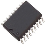
| 描述 | IC DAC 12BIT MULT MONO 18-SOIC数模转换器- DAC IC 12-Bit CMOS Multiplying |
| 产品分类 | |
| 品牌 | Analog Devices Inc |
| 产品手册 | |
| 产品图片 |
|
| rohs | 符合RoHS无铅 / 符合限制有害物质指令(RoHS)规范要求 |
| 产品系列 | 数据转换器IC,数模转换器- DAC,Analog Devices AD7541AKRZ- |
| 数据手册 | |
| 产品型号 | AD7541AKRZ |
| 产品培训模块 | http://www.digikey.cn/PTM/IndividualPTM.page?site=cn&lang=zhs&ptm=19145http://www.digikey.cn/PTM/IndividualPTM.page?site=cn&lang=zhs&ptm=18614http://www.digikey.cn/PTM/IndividualPTM.page?site=cn&lang=zhs&ptm=26125http://www.digikey.cn/PTM/IndividualPTM.page?site=cn&lang=zhs&ptm=26140http://www.digikey.cn/PTM/IndividualPTM.page?site=cn&lang=zhs&ptm=26150http://www.digikey.cn/PTM/IndividualPTM.page?site=cn&lang=zhs&ptm=26147 |
| 产品目录页面 | |
| 产品种类 | 数模转换器- DAC |
| 位数 | 12 |
| 供应商器件封装 | 18-SOIC |
| 分辨率 | 12 bit |
| 包装 | 管件 |
| 商标 | Analog Devices |
| 安装类型 | 表面贴装 |
| 安装风格 | SMD/SMT |
| 封装 | Tube |
| 封装/外壳 | 18-SOIC(0.295",7.50mm 宽) |
| 封装/箱体 | SOIC-18 |
| 工作温度 | 0°C ~ 70°C |
| 工厂包装数量 | 41 |
| 建立时间 | 600ns |
| 接口类型 | Parallel |
| 数据接口 | 并联 |
| 最大功率耗散 | 450 mW |
| 最大工作温度 | + 70 C |
| 最小工作温度 | 0 C |
| 标准包装 | 41 |
| 电压参考 | 10 V |
| 电压源 | 单电源 |
| 电源电压-最大 | 16 V |
| 电源电压-最小 | 5 V |
| 积分非线性 | +/- 0.5 LSB |
| 稳定时间 | 0.6 us |
| 系列 | AD7541A |
| 结构 | R-2R |
| 转换器数 | 1 |
| 转换器数量 | 1 |
| 输出数和类型 | 2 电流 |
| 输出类型 | Current |
| 采样率(每秒) | - |


- 商务部:美国ITC正式对集成电路等产品启动337调查
- 曝三星4nm工艺存在良率问题 高通将骁龙8 Gen1或转产台积电
- 太阳诱电将投资9.5亿元在常州建新厂生产MLCC 预计2023年完工
- 英特尔发布欧洲新工厂建设计划 深化IDM 2.0 战略
- 台积电先进制程称霸业界 有大客户加持明年业绩稳了
- 达到5530亿美元!SIA预计今年全球半导体销售额将创下新高
- 英特尔拟将自动驾驶子公司Mobileye上市 估值或超500亿美元
- 三星加码芯片和SET,合并消费电子和移动部门,撤换高东真等 CEO
- 三星电子宣布重大人事变动 还合并消费电子和移动部门
- 海关总署:前11个月进口集成电路产品价值2.52万亿元 增长14.8%


PDF Datasheet 数据手册内容提取
CMOS, 12-Bit, Monolithic Multiplying DAC Data Sheet AD7541A FEATURES FUNCTIONAL BLOCK DIAGRAM Improved version of the obsoleted product, AD7541 10kΩ 10kΩ 10kΩ VREF Full 4 quadrant multiplication 20kΩ 20kΩ 20kΩ 20kΩ 20kΩ 12-bit linearity (endpoint) S1 S2 S3 S12 All parts guaranteed monotonic TTL/CMOS compatible OUT 2 Protection Schottky diodes not required OUT 1 Low logic input leakage 10kΩ RFEEDBACK BIT 1 (MSB) BIT 2 BIT 3 BIT 12 (LSB) DIGITAL INPUTS (DTL/TTL/CMOS COMPATIBLE) AWPavPeLfoICrmA TgIeOneNrSat ors LOGITICS: DAI GSWITAITLC IHN PISU CTL INO SAE HDI GTOH SIOTUAT T1 EF.OR 00718-001 Figure 1. Analog processing Instrumentation applications Programmable amplifiers and attenuators Digitally controlled calibration Programmable filters and oscillators Composite video Ultrasound Gain, offset, and voltage trimming GENERAL DESCRIPTION PRODUCT HIGHLIGHTS The AD7541A is a high performance, 12-bit monolithic Compatibility—The AD7541A can be used as a direct replacement multiplying digital-to-analog converter (DAC). It is fabricated for any AD7541 type device. As with the AD7541, The digital using advanced, low noise, thin film, complementary metal- inputs on the AD7541A are TTL/CMOS compatible. They have oxide semiconductor (CMOS) technology. The AD7541A is a ±1 µA maximum input current requirement so that they do available in 18-lead PDIP, 18-lead PLCC, and 18-lead SOIC not load the driving circuitry. packages. Improvements—The AD7541A offers the following improved The AD7541A is functionally and pin compatible with the specifications over the AD7541: industry standard AD7541, and it offers improved specifications 1. Gain error for all grades are reduced with premium grade and performance over the obsolete product, AD7541. The versions having a maximum gain error of ±3 LSB. improved design ensures that the AD7541A is latch-up free; 2. Gain error temperature coefficient are reduced to therefore, no output protection Schottky diodes are required. 2 ppm/°C typical and 5 ppm/°C maximum. The AD7541A uses laser wafer trimming to provide full 12-bit 3. Digital-to-analog charge injection energy for the AD7541A endpoint linearity with several high performance grades. is typically 20% less than the standard AD7541. 4. Latch-up proof. 5. Laser wafer trimming provides 1/2 LSB maximum differential nonlinearity for top grade devices over the operating temperature range (vs. 1 LSB on previous AD7541 devices). 6. All grades are guaranteed monotonic to 12 bits over the operating temperature range. Rev. C Document Feedback Information furnished by Analog Devices is believed to be accurate and reliable. However, no responsibility is assumed by Analog Devices for its use, nor for any infringements of patents or other One Technology Way, P.O. Box 9106, Norwood, MA 02062-9106, U.S.A. rights of third parties that may result from its use. Specifications subject to change without notice. No license is granted by implication or otherwise under any patent or patent rights of Analog Devices. Tel: 781.329.4700 ©2017 Analog Devices, Inc. All rights reserved. Trademarks and registered trademarks are the property of their respective owners. Technical Support www.analog.com
AD7541A Data Sheet TABLE OF CONTENTS Features .............................................................................................. 1 Terminology .......................................................................................7 Applications ....................................................................................... 1 Theory of Operation .........................................................................8 Functional Block Diagram .............................................................. 1 Equivalent Circuit Analysis .........................................................8 General Description ......................................................................... 1 Applications Information .................................................................9 Product Highlights ........................................................................... 1 Unipolar Binary Operation (Two Quadrant Multiplication) ......9 Revision History ............................................................................... 2 Bipolar Operation (Four Quadrant Multiplication) .............. 10 Specifications ..................................................................................... 3 Applications Hints ...................................................................... 11 AC Performance Characteristics ................................................ 4 Single-Supply Operation ........................................................... 11 Absolute Maximum Ratings ............................................................ 5 Supplemental Application Material ......................................... 11 ESD Caution .................................................................................. 5 Outline Dimensions ....................................................................... 12 Pin Configurations ........................................................................... 6 Ordering Guide .......................................................................... 13 REVISION HISTORY 3/2017—Rev. B to Rev. C Updated Format .................................................................. Universal Deleted E-20A and Q-18 .............................................. Throughout Added Applications Section ............................................................ 1 Changes to the General Description Section ................................ 1 Changes to Figure 7 .......................................................................... 9 Changes to Bipolar Operation (Four Quadrant Multiplication) Section, Figure 8, and Figure 9 ..................................................... 10 Changes to Figure 10 ...................................................................... 11 Changes to Output Offset Section, Temperature Coefficient Section, Single-Supply Operation Section, and Supplemental Application Material Section ........................................................ 11 Update Outline Dimensions ......................................................... 13 Changes to Ordering Guide .......................................................... 14 Rev. C | Page 2 of 13
Data Sheet AD7541A SPECIFICATIONS V = 15 V, V = 10 V, OUT 1 = OUT 2 = GND = 0 V, unless otherwise noted. Temperature range is as follows for the J version and the DD REF K version: 0°C to +70°C. Table 1. Parameter Version T = 25°C T = T , T Unit Test Conditions/Comments A A MIN MAX ACCURACY Resolution All 12 12 Bits Relative Accuracy J ±1 ±1 LSB max ±1 LSB = ±0.024% of full scale K ±1/2 ±1/2 LSB max ±1/2 LSB = ±0.012% of full scale Differential Nonlinearity J ±1 ±1 LSB max All grades guaranteed monotonic to K ±1/2 ±1/2 LSB max 12 bits, TMIN to TMAX. Gain Error J ±6 ±8 LSB max Measured using internal R and FEEDBACK K ±3 ±5 LSB max includes effect of leakage current and gain temperature coefficient (TC); gain error can be trimmed to zero Gain TC1 ΔGain/ΔTemperature All 5 5 ppm/°C max Typical value is 2 ppm/°C Output Leakage Current OUT 1 (Pin 1) J, K ±5 ±10 nA max All digital inputs = 0 V OUT 2 (Pin 2) J, K ±5 ±10 nA max All digital inputs = V DD REFERENCE INPUT Input Resistance (Pin 17 to All 7 to 18 7 to 18 kΩ min/max Typical input resistance = 11 kΩ; typical GND) input resistance TC = −300 ppm/°C DIGITAL INPUTS Input Voltage High, V All 2.4 2.4 V min IH Low, V All 0.8 0.8 V max IL Input Current, I All ±1 ±1 µA max Logic inputs are MOS gates; IN I typical (25°C) = 1 nA IN Input Capacitance, C 1 All 8 8 pF max V = 0 V IN IN POWER SUPPLY REJECTION ΔGain/ΔV All ±0.01 ±0.02 % per % max ΔV = ±5% DD DD POWER SUPPLY V Range All 5 to 16 5 to 16 V min/V max Accuracy is not guaranteed over this range DD I All 2 2 mA max All digital inputs V or V DD IL IH 100 500 µA max All digital inputs 0 V or V DD 1 Guaranteed by design but not production tested. Rev. C | Page 3 of 13
AD7541A Data Sheet AC PERFORMANCE CHARACTERISTICS These characteristics are included for design guidance only and are not subject to test. V = 15 V, V = 10 V, and OUT 1 = OUT 2 = GND = 0 V, DD IN unless otherwise noted. Temperature range is as follows for the J version and the K version: 0°C to +70°C. Table 2. Parameter T = 25°C T = T ,T Unit Test Conditions/Comments A A MIN MAX PROPAGATION DELAY (FROM DIGITAL INPUT 100 ns typ OUT 1 load = 100 Ω, C = 13 pF; digital inputs EXT CHANGE TO 90% OF FINAL ANALOG OUTPUT) = 0 V to V or V to 0 V DD DD DIGITAL-TO-ANALOG GLITCH IMPULSE 1000 nV-sec typ V = 0 V; all digital inputs 0 V to V or V to 0 V; REF DD DD measured using Model 50K as output amplifier MULTIPLYING FEEDTHROUGH ERROR (V to 1.0 mV p-p typ V = ±10 V, 10 kHz sine wave REF REF OUT 1) OUTPUT CURRENT SETTLING TIME 0.6 µs typ To 0.01% of full-scale range; OUT 1 load = 100 Ω, C = 13 pF; digital inputs = 0 V to V or V to 0 V EXT DD DD OUTPUT CAPACITANCE C (Pin 1) 200 200 pF max Digital inputs = V OUT 1 IH 70 70 pF max Digital inputs = V IL C (Pin 2) 70 70 pF max Digital inputs = V OUT 2 IH 200 200 pF max Digital inputs = V IL Rev. C | Page 4 of 13
Data Sheet AD7541A ABSOLUTE MAXIMUM RATINGS Stresses at or above those listed under Absolute Maximum T = 25°C, unless otherwise noted. A Ratings may cause permanent damage to the product. This is a Table 3. stress rating only; functional operation of the product at these Parameter Rating or any other conditions above those indicated in the operational V to GND 17 V section of this specification is not implied. Operation beyond DD V to GND ±25 V the maximum operating conditions for extended periods may REF V to GND ±25 V affect product reliability. RFEEDBACK Digital Input Voltage to GND −0.3 V, V + 0.3 V DD OUT 1, OUT 2 to GND −0.3 V, V + 0.3 V DD ESD CAUTION Power Dissipation (Any Package) To 75°C 450 mW Derates Above 75°C 6 mW/°C Operating Temperature Range Commercial (J Version/K Version) 0°C to 70°C Storage Temperature −65°C to +150°C Lead Temperature (Soldering, 10 secs) 300°C Rev. C | Page 5 of 13
AD7541A Data Sheet PIN CONFIGURATIONS OUT 1 1 18 RFEEDBACK OUT 2 2 17 VREF IN GND 3 16 VDD (+) BIT 1 (MSB) 4 AD7541A 15 BIT 12 (LSB) BIT 2 5 TOP VIEW 14 BIT 11 (Not to Scale) BIT 3 6 13 BIT 10 BIT 4 7 12 BIT 8 BBIITT 56 89 1110 BBIITT 87 00718-002 Figure 2. 18-Lead PDIP and 18-Lead SOIC Pin Configuration K C A B 2 1 D OUT OUT NC RFEEVREF 3 2 1 20 19 GND4 18VDD BIT 1 (MSB)5 AD7541A 17BIT 12 (LSB) BIT 26 16BIT 11 TOP VIEW BIT 37 (Not to Scale) 15BIT 10 BIT 48 14BIT 9 9 10 11 12 13 5 6 C 7 8 T T N T T N1.O NTCE S= NBIO BICONNEBICT.BI 00718-003 Figure 3. 20-Lead PLCC Pin Configuration Rev. C | Page 6 of 13
Data Sheet AD7541A TERMINOLOGY Output Leakage Current Relative Accuracy Current that appears at OUT I with the DAC loaded to all 0s or Relative accuracy or endpoint nonlinearity is a measure of the at OUT 2 with the DAC loaded to all 1s. maximum deviation from a straight line passing through the endpoints of the DAC transfer function. It is measured after Multiplying Feedthrough Error adjusting for zero scale and full scale, and it is expressed in % of AC error due to capacitive feedthrough from the V terminal REF full-scale range or (sub) multiples of 1 LSB. to OUT 1 with the DAC loaded to all 0s. Differential Nonlinearity Output Current Settling Time Differential nonlinearity is the difference between the measured Time required for the output function of the DAC to settle to change and the ideal l LSB change between any two adjacent within 1/2 LSB for a given digital input stimulus, that is, 0 to codes. A specified differential nonlinearity of ±1 LSB maximum full scale. over the operating temperature range ensures monotonicity. Propagation Delay Gain Error The propagation delay is a measure of the internal delay of the Gain error is a measure of the output error between an ideal circuit, and it is measured from the time a digital input changes DAC and the actual device output. For the AD7541A, ideal to the point at which the analog output at OUT 1 reaches 90% maximum output is of its final value. −(4095/4096)(V ) Digital-to-Analog Glitch Impulse (QDA) REF The QDA is a measure of the amount of charge injected from Gain error is adjustable to zero using external trims, as shown the digital inputs to the analog outputs when the inputs change in Figure 7, Figure 8, and Figure 9. state. It is usually specified as the area of the glitch in nV-sec and is measured with V = GND and a Model 50K as the REF output op amp, C1 (phase compensation) = 0 pF. Rev. C | Page 7 of 13
AD7541A Data Sheet THEORY OF OPERATION The simplified digital-to-analog circuit is shown in Figure 4. An EQUIVALENT CIRCUIT ANALYSIS inverted R-2R ladder structure was used, meaning the binarily The equivalent circuits for all digital inputs low and all digital weighted currents are switched between the OUT 1 and OUT 2 inputs high are shown in Figure 5 and Figure 6. In Figure 5 with bus lines, thus maintaining a constant current in each ladder leg all digital inputs low, the reference current is switched to OUT 2. independent of the switch state. The current source, I , is composed of surface and junction LEAKAGE VREF 10kΩ 10kΩ 10kΩ leakages to the substrate, while the I/4096 current source represents a constant 1-bit current drain through the termination resistor on 20kΩ 20kΩ 20kΩ 20kΩ 20kΩ the R-2R ladder. The on capacitance of the output N-channel S1 S2 S3 S12 switch is 200 pF, as shown on the OUT 2 terminal. The off OUT 2 switch capacitance is 70 pF, as shown on the OUT 1 terminal. OUT 1 Analysis of the circuit for all digital inputs high, as shown in 10kΩ RFEEDBACK Figure 5, is similar to Figure 4; however, the on switches are BIT 1 (MSB) BIT 2 BIT 3 BIT 12 (LSB) now on the OUT 1 terminal; therefore, 200 pF at that terminal. DIGITAL INPUTS (DTL/TTL/CMOS COMPATIBLE) LOGITICS: DAI GSWITAITLC IHN PISU CTL INO SAE HDI GTOH SIOTUAT T1 EF.OR 00718-005 R ROFUETE D1BACK Figure 4. Functional Diagram (Inputs High) ILEAKAGE 70pF The input resistance at V (see Figure 4) is always equal to REF R≈ 15kΩ RLDR, which is the R-2R ladder characteristic resistance and is VREF OUT 2 reeqfuearel ntoc ev atelurme Rin. aBl eccaanu bsee RdrINiv aetn t hbey Va RrEeFf eprienn icse c voonlsttaagnet ,o trh ae IREF I/4096 ILEAKAGE 200pF 00718-006 reference current, ac or dc, of positive or negative polarity. If a Figure 5. DAC Equivalent Circuit, All Digital Inputs Low current source is used, a low temperature coefficient external R R is recommended to define the scale factor. R≈ 15kΩ RFEEDBACK FEEDBACK VREF OUT 1 IREF I/4096 ILEAKAGE 200pF OUT 2 ILEAKAGE 70pF 00718-007 Figure 6. DAC Equivalent Circuit All Digital Inputs High Rev. C | Page 8 of 13
Data Sheet AD7541A APPLICATIONS INFORMATION UNIPOLAR BINARY OPERATION (TWO QUADRANT C1 phase compensation (10 pF to 25 pF) may be required for MULTIPLICATION) stability when using high speed amplifiers. C1 is used to cancel the pole formed by the DAC internal feedback resistance and Figure 7 shows the analog circuit connections required for output capacitance at OUT 1. unipolar binary (two quadrant multiplication) operation. With a dc reference voltage or current (positive or negative polarity) Amplifier A1 must be selected or trimmed to provide VOS ≤ 10% of applied at Pin 17, the circuit is a unipolar DAC. With an ac the voltage resolution at VOUT. Additionally, the amplifier must reference voltage or current, the circuit provides two quadrant exhibit a bias current that is low over the temperature range of multiplication (digitally controlled attenuation). The input/output interest (bias current causes output offset at VOUT equal to IB relationship is shown in Table 5. times the DAC feedback resistance, nominally 11 kΩ). VDD R21 Table 4. Recommended Trim Resistor Values vs. Grades C1 Trim Resistor JN KN 16 18 33pF VDD RFEEDBACK R1 100 Ω 100 Ω VIN R11 17 VREF INAD7541A OUT 1 1 VOUT R2 47 Ω 33 Ω PIN 4 TO OUT 2 2 PIN 15 GND Table 5. Unipolar Binary Code Table for Circuit of Figure 7 4 15 2 Binary Number in DAC MSB LSB Analog Output, V BIT 1 TO DIGITAL ANALOG OUT 1REFERB ITTO 1 2TABLGE R4OUND COMMON 00718-008 11 10 10 10 10 10 10 10 0 0 0 0 −−VVIINN((42009458//44009966)) = −1/2VIN Figure 7. Unipolar Binary Operation 0 0 0 0 0 0 0 0 0 0 0 1 −V (1/4096) IN R1 provides full-scale trim capability (that is, load the DAC 0 0 0 0 0 0 0 0 0 0 0 0 0 V register to 1111 1111 1111, adjust R1 for VOUT = –VREF (4095/4096)). Alternatively, full scale can be adjusted by omitting R1 and R2 and trimming the reference voltage magnitude. Rev. C | Page 9 of 13
AD7541A Data Sheet BIPOLAR OPERATION (FOUR QUADRANT Figure 9 and Table 7 show an alternative method of achieving MULTIPLICATION) bipolar output. The circuit operates with sign plus magnitude code and has the advantage of giving 12-bit resolution in each Figure 8 and Table 6 illustrate the circuitry and code relationship quadrant, compared with 11-bit resolution per quadrant for the for bipolar operation. With a dc reference (positive or negative circuit of Figure 8. The ADG5436F is a dual SPDT, latch-up polarity), the circuit provides offset binary operation. With an immune switch. R4 and R5 must match each other to 0.01% to ac reference, the circuit provides full four quadrant multiplication. maintain the accuracy of the DAC. Mismatch between R4 and With the DAC loaded to 1000 0000 0000, adjust R1 for V = OUT R5 introduces a gain error. 0 V (alternatively, omit R1 and R2 and adjust the ratio of R3 to R4 for V = 0 V). To accomplish, full-scale trimming, adjust Table 7. 12-Bit Plus Sign Magnitude Code Table for Circuit OUT the amplitude of V or vary the R5 value. of Figure 9 REF Binary Number in DAC As in unipolar operation, A1 must be chosen for low V and OS Sign Bit1 MSB LSB Analog Output, V low I. R3, R4, and R5 must be selected for matching and tracking. OUT B 0 1 1 1 1 1 1 1 1 1 1 1 1 +V × (4095/4096) Mismatch of R3 to R4 causes both offset and full-scale error. IN 0 0 0 0 0 0 0 0 0 0 0 0 0 0 V Mismatch of R5 to R4 or R3 causes full-scale error. C1 phase 1 0 0 0 0 0 0 0 0 0 0 0 0 0 V compensation (10 pF to 50 pF) may be required for stability, 1 1 1 1 1 1 1 1 1 1 1 1 1 −V × (4095/4096) depending on amplifier used. IN 1 When the sign bit equals 0, it connects R3 to GND. Table 6. Bipolar Code Table for Offset Binary Circuit of Figure 8 Binary Number in DAC MSB LSB Analog Output, V OUT 1 1 1 1 1 1 1 1 1 1 1 1 +VIN(2047/2048) 1 0 0 0 0 0 0 0 0 0 0 1 +V (1/2048) IN 1 0 0 0 0 0 0 0 0 0 0 0 0 V 0 1 1 1 1 1 1 1 1 1 1 1 −V (1/2048) IN 0 0 0 0 0 0 0 0 0 0 0 0 −V (2048/2048) IN VDD R21 R4 R5 C1 20kΩ 20kΩ 16 18 33pF VDD RFEEDBACK R3 VIN R11 17 VREFAD7541AOUT 1 1 A1 10kΩ PIN 4 TO OUT 2 2 A2 VOUT PIN 15 DGND R6 4 15 2 5kΩ 10% BIT 1 TO DIGITAL ANALOG 1SFOEER TVBAAIBTLL U1EE2 S4. OGF RRO1 UANNDD R2,COMMON 00718-009 Figure 8. Bipolar Operation (Four-Quadrant Multiplication) VDD R21 R4 R5 16 18 C331pF 20kΩ 20kΩ VDD RFEEDBACK VIN R11 17 VREFAD7541A OUT 1 1 A1 A2 VOUT PIN 4 TO OUT 2 2 R3 PIN 15 DGND 10kΩ 4 15 2 1/2 10% ADG5436F DIGITAL ANALOG GROUND COMMON BIT 1 TO BIT 12 1SFOEER TVAABLLUEE S4. OF R1 AND R2, 00718-010 Figure 9. 12-Bit Plus Sign Magnitude Operation Rev. C | Page 10 of 13
Data Sheet AD7541A APPLICATIONS HINTS SINGLE-SUPPLY OPERATION Output Offset Figure 10 shows the AD7541A connected in a voltage switching The CMOS DACs exhibit a code dependent, output resistance mode. OUT 1 is connected to the reference voltage, and OUT 2 that can cause a code dependent error voltage at the output of is connected to GND. The output voltage of the DAC is available at the amplifier. The maximum amplitude of this offset, which the VREF pin (Pin 17) and has a constant output impedance equal to adds to the nonlinearity of the DAC, is 0.67 VOS, where VOS is RLDR. The feedback resistor, RFEEDBACK, is not used in this circuit. the amplifier input offset voltage. To maintain monotonic VDD = 15V NOT USED operation, it is recommended that V be no greater than OS 18 16 (25 × 10–6) × VREF over the temperature range of operation. RFEEDBACKVDD Suitable op amps include the following: OP27, OP177, and OP777. V2R.5EVF 1 OUT 1 AD7541AVREF 17 V+ VOUT = 0V TO 10V The OP27 is best suited for fixed reference applications with 2 OUT 2 PIN 4 TO V– GND PIN 15 low bandwidth requirements. The OP27 has extremely low 2 4 15 R2 offset (25 µV), and does not require an offset trim in most 30kΩ applications. The AD711 has a much wider bandwidth and R1 BIT 1 TO BIT 12 10kΩ higher slew rate and is recommended for multiplying and SYSTEM other applications that require fast settling. VTHOUATT ±IS V,R DE FIS D A ( 1F +R ARC2/TRIO1)N WAHL ERREEP R0 E≤SDE ≤NT1A,TION OF THE DIGITAL INGPRUOTUND 00718-011 Digital Glitches Figure 10. Single Supply Operation Using Voltage Switching Mode One cause of digital glitches is capacitive coupling from the digital The reference voltage must always be positive. If OUT 1 goes lines to the OUT 1 and OUT 2 terminals. This coupling can be more than 0.3 V less than GND, an internal diode is turned on minimized by screening the analog pins of the AD7541A (Pin 1, and a heavy current may flow, causing device damage (the Pin 2, Pin 17, and Pin 18) from the digital pins by a ground track AD7541A is protected from the SCR latch-up phenomenon run between Pin 2 and Pin 3 and between Pin 16 and Pin 17 of prevalent in many CMOS devices). Suitable references include the AD7541A. Note how the analog pins are at one end of the the ADR431, the ADR441, and the REF192. package and are separated from the digital pins by V and DD The loading on the reference voltage source is code dependent, GND to aid screening at the board level. On-chip capacitive and the behavior of the reference voltage with changing load coupling can also give rise to crosstalk from the digital to conditions often determines the response time of the circuit. analog sections of the AD7541A, particularly in circuits with To maintain linearity, the voltage at OUT 1 must remain within high currents and fast rise and fall times. 2.5 V of GND for a V of 15 V. If V is reduced from 15 V, or DD DD Temperature Coefficients if the reference voltage at OUT 1 is increased to more than 2.5 V, The gain temperature coefficient of the AD7541A has a maximum the differential nonlinearity of the DAC increases, and the value of 5 ppm/°C and a typical value of 2 ppm/°C. This coefficient linearity of the DAC degrades. corresponds to worst case gain shifts of 2 LSB and 0.8 LSB, SUPPLEMENTAL APPLICATION MATERIAL respectively, over a 100°C temperature range. When trim resistors, For further information on CMOS multiplying DACs, refer to R1 and R2, are used to adjust the full-scale range, the temperature the following: coefficients of R1 and R2 must also be taken into account. Analog-Digital Conversion Handbook, 1972, Analog Devices, Inc. CMOS DAC Application Guide, 1984, Analog Devices Analog-Digital Conversion Handbook, 1986, Analog Devices Rev. C | Page 11 of 13
AD7541A Data Sheet OUTLINE DIMENSIONS 0.180 (4.57) 0.048 (1.22 ) 0.165 (4.19) 0.042 (1.07) 0.056 (1.42) 0.042 (1.07) 0M.2IN0 (0.51) 0.020R (0.50) 3 19 0.021 (0.53) 00..004482 ((11..2027)) 4 IDEPNITNI F1IER 18 (01.0.2570) 0.013 (0.33)0.330 (8.38) BOTTOM TOP VIEW BSC 0.032 (0.81)0.290 (7.37) VIEW (PINS DOWN) 0.026 (0.66) (PINS UP) 8 14 9 13 0.020 0.045 (1.14) (0.R51) 00..335560 ((98..0849))SQ 0.025 (0.64) R 0.120 (3.04) 0.395 (10.03)SQ 0.090 (2.29) 0.385 (9.78) COMPLIANT TO JEDEC STANDARDS MO-047-AA CONTROLLING DIMENSIONS ARE IN INCHES; MILLIMETER DIMENSIONS (IN PARENTHESES) ARE ROUNDED-OFF INCH EQUIVALENTS FOR REFERENCE ONLY AND ARE NOT APPROPRIATE FOR USE IN DESIGN. Figure 11. 20-Lead Plastic Leadless Chip Carrier [PLCC] (P-20) Dimensions shown in inches and (millimeters) 0.920 (23.37) 0.900 (22.86) 0.880 (22.35) 18 10 0.280 (7.11) 0.250 (6.35) 1 9 0.240 (6.10) 0.325 (8.26) 0.310 (7.87) 0.100 (2.54) 0.300 (7.62) BSC 0.060 (1.52) 0.195 (4.95) 0.210 (5.33) MAX 0.130 (3.30) MAX 0.115 (2.92) 0.015 0.150 (3.81) (0.38) 0.015 (0.38) 0.130 (3.30) MIN GAUGE 0.115 (2.92) SEATING PLANE 0.014 (0.36) PLANE 0.010 (0.25) 0.022 (0.56) 0.008 (0.20) 0.005 (0.13) 0.430 (10.92) 0.018 (0.46) MIN MAX 0.014 (0.36) 0.070 (1.78) 0.060 (1.52) 0.045 (1.14) COMPLIANTTO JEDEC STANDARDS MS-001 CONTROLLING DIMENSIONSARE IN INCHES; MILLIMETER DIMENSIONS (RCINEOFRPEANRREERENN LCTEEHA EODSNSEL MSY)AAAYNR BDEE AR CROOEU NNNFODIGETUDAR-POEPFDRFOA INSPC RWHIAH ETOEQL UFEIO VORAR LU EHSNAETL ISFN FLDOEEARSDIGSN.. 070706-A Figure 12. 18-Lead Plastic Dual In-Line Package [PDIP] (N-18) Dimensions shown in inches and (millimeters) Rev. C | Page 12 of 13
Data Sheet AD7541A 11.75 (0.4626) 11.35 (0.4469) 18 10 7.60 (0.2992) 7.40 (0.2913) 1 9 10.65 (0.4193) 10.00 (0.3937) 0.75 (0.0295) 45° 2.65 (0.1043) 0.25 (0.0098) 0.30 (0.0118) 2.35 (0.0925) 8° 0.10 (0.0039) 0° COPLANARITY 0.10 (0.10.52070) 00..5311 ((00..00210212)) SPLEAATNIENG 00..3230 ((00..00103709)) 10..2470 ((00..00510507)) BSC COMPLIANTTO JEDEC STANDARDS MS-013-AB C(RINEOFNPEATRRREOENNLCLTEIHN EOGSN EDLSIYM)AEANNRDSEI AORRNOESU NANORDEET DAIN-PO MPFRIFLO LMPIIMRLELIATIMTEEER TFSEO; RIRN ECUQHSU EDI VIINMA LEDENENSSTIIOGSN NFS.OR 060706-A Figure 13. 18-Lead Standard Small Outline Package [SOIC_W] (RW-18) Dimensions shown in millimeters and (inches) ORDERING GUIDE Model1 Temperature Range Relative Accuracy, T to T Error, T = 25°C Package Description Package Option MIN MAX A AD7541AJNZ 0°C to +70°C ±1 LSB ±6 LSB 18-Lead PDIP N-18 AD7541AKNZ 0°C to +70°C ±1/2 LSB ±3 LSB 18-Lead PDIP N-18 AD7541AJPZ-REEL 0°C to +70°C ±1 LSB ±6 LSB 20-Lead PLCC P-20 AD7541AKPZ-REEL 0°C to +70°C ±1/2 LSB ±3 LSB 20-Lead PLCC P-20 AD7541AKR 0°C to +70°C ±1/2 LSB ±3 LSB 18-Lead SOIC_W RW-18 AD7541AKRZ 0°C to +70°C ±1/2 LSB ±3 LSB 18-Lead SOIC_W RW-18 AD7541AKRZ-REEL 0°C to +70°C ±1/2 LSB ±3 LSB 18-Lead SOIC_W RW-18 AD7541AKRZ–REEL7 0°C to +70°C ±1/2 LSB ±3 LSB 18-Lead SOIC_W RW-18 AD7541AACHIPS DIE 1 Z = RoHS Compliant Part. ©2017 Analog Devices, Inc. All rights reserved. Trademarks and registered trademarks are the property of their respective owners. D00718-0-3/17(C) Rev. C | Page 13 of 13