ICGOO在线商城 > 集成电路(IC) > 数据采集 - 模数转换器 > AD7476ARTZ-500RL7
 Datasheet下载
- 型号: AD7476ARTZ-500RL7
- 制造商: Analog
- 库位|库存: xxxx|xxxx
- 要求:
| 数量阶梯 | 香港交货 | 国内含税 |
| +xxxx | $xxxx | ¥xxxx |
查看当月历史价格
查看今年历史价格
AD7476ARTZ-500RL7产品简介:
ICGOO电子元器件商城为您提供AD7476ARTZ-500RL7由Analog设计生产,在icgoo商城现货销售,并且可以通过原厂、代理商等渠道进行代购。 AD7476ARTZ-500RL7价格参考。AnalogAD7476ARTZ-500RL7封装/规格:数据采集 - 模数转换器, 12 Bit Analog to Digital Converter 1 Input 1 SAR SOT-23-6。您可以下载AD7476ARTZ-500RL7参考资料、Datasheet数据手册功能说明书,资料中有AD7476ARTZ-500RL7 详细功能的应用电路图电压和使用方法及教程。
AD7476ARTZ-500RL7是Analog Devices Inc.生产的一款12位、500ksps(每秒千采样)的逐次逼近型模数转换器(SAR ADC),采用小型8引脚TSOT封装,具备低功耗和高精度特性。该器件广泛应用于对空间、功耗和性能有较高要求的便携式与工业级数据采集系统。

典型应用场景包括:便携式医疗设备(如血糖仪、心电图机、血压计等),用于将生物模拟信号精确转换为数字信号;工业自动化中的传感器信号采集,如温度、压力、湿度等参数监测;电池供电的现场仪表和智能传感器模块,得益于其低功耗特性,适合长时间运行;通信系统中用于信号监控与调理;以及消费类电子设备中的精密测量单元。

AD7476ARTZ-500RL7支持单电源供电(2.7V至5.25V),输入模拟信号范围可配置为单端或伪差分模式,配合内部基准电压源或外部参考,确保转换精度。其集成的片上采样保持电路和SPI兼容串行接口,简化了系统设计,提高了可靠性。此外,该器件符合RoHS标准,适用于对环保要求较高的产品。

综上,AD7476ARTZ-500RL7凭借高分辨率、快速采样、小尺寸和低功耗优势,特别适用于紧凑型、高精度的数据采集系统,在医疗、工业、通信和便携设备领域具有广泛应用价值。
| 参数 | 数值 |
| 产品目录 | 集成电路 (IC)半导体 |
| 描述 | IC ADC 12BIT 1MSPS SOT-23-6模数转换器 - ADC 12Bit 1MSPS Lo-Pwr |
| 产品分类 | |
| 品牌 | Analog Devices Inc |
| 产品手册 | |
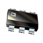
| 产品图片 |
|
| rohs | 符合RoHS无铅 / 符合限制有害物质指令(RoHS)规范要求 |
| 产品系列 | 数据转换器IC,模数转换器 - ADC,Analog Devices AD7476ARTZ-500RL7- |
| 数据手册 | |
| 产品型号 | AD7476ARTZ-500RL7 |
| 产品目录页面 | |
| 产品种类 | 模数转换器 - ADC |
| 位数 | 12 |
| 供应商器件封装 | SOT-23-6 |
| 信噪比 | 72.5 dB |
| 其它名称 | AD7476ARTZ-500RL7DKR |
| 分辨率 | 12 bit |
| 包装 | Digi-Reel® |
| 商标 | Analog Devices |
| 安装类型 | 表面贴装 |
| 安装风格 | SMD/SMT |
| 封装 | Reel |
| 封装/外壳 | SOT-23-6 |
| 封装/箱体 | SOT-23-6 |
| 工作温度 | -40°C ~ 85°C |
| 工作电源电压 | 5 V |
| 工厂包装数量 | 500 |
| 接口类型 | Serial (SPI, QSPI, Microwire) |
| 数据接口 | DSP,MICROWIRE™,QSPI™,串行,SPI™ |
| 最大功率耗散 | 17.5 mW |
| 最大工作温度 | + 125 C |
| 最小工作温度 | - 55 C |
| 标准包装 | 1 |
| 特性 | - |
| 电压参考 | External |
| 电压源 | 单电源 |
| 系列 | AD7476 |
| 结构 | SAR |
| 设计资源 | 点击此处下载产品Datasheet点击此处下载产品Datasheet点击此处下载产品Datasheet点击此处下载产品Datasheet点击此处下载产品Datasheet点击此处下载产品Datasheet |
| 转换器数 | 1 |
| 转换器数量 | 1 |
| 转换速率 | 1 MS/s |
| 输入数和类型 | 1 个单端,单极 |
| 输入类型 | Single-Ended |
| 通道数量 | 1 Channel |
| 配用 | /product-detail/zh/EVAL-AD7476ACBZ/EVAL-AD7476ACBZ-ND/1679967 |
| 采样率(每秒) | 1M |


- 商务部:美国ITC正式对集成电路等产品启动337调查
- 曝三星4nm工艺存在良率问题 高通将骁龙8 Gen1或转产台积电
- 太阳诱电将投资9.5亿元在常州建新厂生产MLCC 预计2023年完工
- 英特尔发布欧洲新工厂建设计划 深化IDM 2.0 战略
- 台积电先进制程称霸业界 有大客户加持明年业绩稳了
- 达到5530亿美元!SIA预计今年全球半导体销售额将创下新高
- 英特尔拟将自动驾驶子公司Mobileye上市 估值或超500亿美元
- 三星加码芯片和SET,合并消费电子和移动部门,撤换高东真等 CEO
- 三星电子宣布重大人事变动 还合并消费电子和移动部门
- 海关总署:前11个月进口集成电路产品价值2.52万亿元 增长14.8%


PDF Datasheet 数据手册内容提取
1 MSPS, 12-/10-/8-Bit ADCs in 6-Lead SOT-23 AD7476/AD7477/AD7478 FEATURES FUNCTIONAL BLOCK DIAGRAM Fast throughput rate: 1 MSPS VDD Specified for V of 2.35 V to 5.25 V DD Low power 12-/10-/8-BIT 3.6 mW at 1 MSPS with 3 V supplies VIN APSPURCOCXEISMSAIVTEIO-N 15 mW at 1 MSPS with 5 V supplies ADC Wide input bandwidth 70 dB SNR at 100 kHz input frequency SCLK Flexible power/serial clock speed management COLNOTGRICOL SDATA No pipeline delays CS High speed serial interface AD7476/AD7477/AD7478 SPI®-/QSPI™-/MICROWIRE™-/DSP-compatible Standby mode: 1 μA maximum GND 01024-001 6-lead SOT-23 package Figure 1. APPLICATIONS Battery-powered systems Personal digital assistants Medical instruments Mobile communications Instrumentation and control systems Data acquisition systems High speed modems Optical sensors GENERAL DESCRIPTION PRODUCT HIGHLIGHTS The AD7476/AD7477/AD74781 are, respectively, 12-bit, 10-bit, 1. First 12-/10-/8-Bit ADCs in SOT-23 Packages. and 8-bit, high speed, low power, successive approximation 2. High Throughput with Low Power Consumption. ADCs. The parts operate from a single 2.35 V to 5.25 V power supply and feature throughput rates up to 1 MSPS. Each part 3. Flexible Power/Serial Clock Speed Management. The contains a low noise, wide bandwidth track-and-hold amplifier conversion rate is determined by the serial clock, allowing that can handle input frequencies in excess of 6 MHz. the conversion time to be reduced through the serial clock speed increase. This allows the average power consumption The conversion process and data acquisition are controlled to be reduced while not converting. The parts also feature a using CS and the serial clock, allowing the devices to interface shutdown mode to maximize power efficiency at lower with microprocessors or DSPs. The input signal is sampled on throughput rates. Current consumption is 1 μA maximum the falling edge of CS and the conversion is initiated at this when in shutdown mode. point. There are no pipeline delays associated with these parts. 4. Reference Derived from the Power Supply. The AD7476/AD7477/AD7478 use advanced design techniques to achieve very low power dissipation at high throughput rates. 5. No Pipeline Delay. The parts feature a standard successive- The reference for the parts is taken internally from V . This approximation ADC with accurate control of the sampling DD allows the widest dynamic input range to the ADC. Thus, the instant via a CS input and once-off conversion control. analog input range for the parts are 0 V to V . The conversion DD rate is determined by the SCLK. 1 Protected by U.S. Patent No. 6,681,332. Rev. F Information furnished by Analog Devices is believed to be accurate and reliable. However, no responsibility is assumed by Analog Devices for its use, nor for any infringements of patents or other One Technology Way, P.O. Box 9106, Norwood, MA 02062-9106, U.S.A. rights of third parties that may result from its use. Specifications subject to change without notice. No license is granted by implication or otherwise under any patent or patent rights of Analog Devices. Tel: 781.329.4700 www.analog.com Trademarks and registered trademarks are the property of their respective owners. Fax: 781.461.3113 ©2000–2009 Analog Devices, Inc. All rights reserved.
AD7476/AD7477/AD7478 TABLE OF CONTENTS Features .............................................................................................. 1 Typical Performance Characteristics ........................................... 11 Applications ....................................................................................... 1 Terminology .................................................................................... 12 Functional Block Diagram .............................................................. 1 Theory of Operation ...................................................................... 13 General Description ......................................................................... 1 Circuit Information .................................................................... 13 Product Highlights ........................................................................... 1 Converter Operation .................................................................. 13 Revision History ............................................................................... 2 ADC Transfer Function ............................................................. 13 Specifications ..................................................................................... 3 Typical Connection Diagram ................................................... 14 AD7476 Specifications ................................................................. 3 Modes of Operation ................................................................... 15 AD7477 Specifications ................................................................. 5 Power vs. Throughput Rate ....................................................... 17 AD7478 Specifications ................................................................. 7 Serial Interface ............................................................................ 18 Timing Specifications .................................................................. 8 Microprocessor Interfacing ....................................................... 19 Absolute Maximum Ratings ............................................................ 9 Outline Dimensions ....................................................................... 21 ESD Caution .................................................................................. 9 Ordering Guide .......................................................................... 22 Pin Configuration and Function Descriptions ........................... 10 REVISION HISTORY 1/09—Rev. E to Rev. F 3/04—Rev. C to Rev. D Added U.S. Patent Number .............................................................. 1 Changes to Features .......................................................................... 1 Changes to Specifications ................................................................. 2 Changes to Ordering Guide .......................................................... 22 Changes to Absolute Maximum Ratings ........................................ 6 4/06—Rev. D to Rev. E Changes to AD7476/AD7477/AD7478 to ADSP-21xx Updated Format .................................................................. Universal Interface section .............................................................................. 16 Changes to Table 1 Endnotes .......................................................... 3 Changes to Table 2 Endnotes .......................................................... 5 2/03—Rev. B to Rev. C Changes to Table 3 Endnotes .......................................................... 7 Changes to General Description ..................................................... 1 Updated Outline Dimensions ....................................................... 21 Changes to Specifications ................................................................. 2 Changes to Ordering Guide .......................................................... 22 Changes to Absolute Maximum Ratings ........................................ 6 Changes to Ordering Guide ............................................................. 6 Changes to Typical Connection Diagram section ..................... 10 Changes to Figure 8 caption .......................................................... 11 Changes to Figure 19 ...................................................................... 16 Changes to Figure 20 ...................................................................... 17 Updated Outline Dimensions ....................................................... 18 Rev. F | Page 2 of 24
AD7476/AD7477/AD7478 SPECIFICATIONS AD7476 SPECIFICATIONS A version: V = 2.7 V to 5.25 V, f = 20 MHz, f = 1 MSPS, unless otherwise noted; S and B versions: V = 2.35 V to 5.25 V, DD SCLK SAMPLE DD f = 12 MHz, f = 600 kSPS, unless otherwise noted; T = T to T , unless otherwise noted. SCLK SAMPLE A MIN MAX Table 1. Parameter A Version1,2 B Version1,2 S Version1,2 Unit Test Conditions/Comments DYNAMIC PERFORMANCE f = 100 kHz sine wave IN Signal-to-(Noise + Distortion) (SINAD)3 69 70 69 dB min B version, V = 2.4 V to 5.25 V DD 70 70 dB min T = 25°C A 71.5 dB typ Signal-to-Noise Ratio (SNR)3 70 71 70 dB min B version, V = 2.4 V to 5.25 V DD 72.5 dB typ Total Harmonic Distortion (THD)3 −80 −78 −78 dB typ Peak Harmonic or Spurious Noise (SFDR)3 −82 −80 −80 dB typ Intermodulation Distortion (IMD)3 Second-Order Terms −78 −78 −78 dB typ fa = 103.5 kHz, fb = 113.5 kHz Third-Order Terms −78 −78 −78 dB typ fa = 103.5 kHz, fb = 113.5 kHz Aperture Delay 10 10 10 ns typ Aperture Jitter 30 30 30 ps typ Full Power Bandwidth 6.5 6.5 6.5 MHz typ @ 3 dB DC ACCURACY S, B versions, V = (2.35 V to 3.6 V)4; DD A version, V = (2.7 V to 3.6 V) DD Resolution 12 12 12 Bits Integral Nonlinearity3 ±1.5 ±1.5 LSB max ±1 ±0.6 ±0.6 LSB typ Differential Nonlinearity3 −0.9/+1.5 −0.9/+1.5 LSB max Guaranteed no missed codes to 12 bits ±0.75 ±0.75 ±0.75 LSB typ Offset Error3 ±1.5 ±2 LSB max ±0.5 LSB typ Gain Error3 ±1.5 ±2 LSB max ±0.5 LSB typ ANALOG INPUT Input Voltage Ranges 0 to V 0 to V 0 to V V DD DD DD DC Leakage Current ±1 ±1 ±1 μA max Input Capacitance 30 30 30 pF typ LOGIC INPUT Input High Voltage, V 2.4 2.4 2.4 V min INH 1.8 1.8 1.8 V min V = 2.35 V DD Input Low Voltage, V 0.4 0.4 0.4 V max V = 3 V INL DD 0.8 0.8 0.8 V max V = 5 V DD Input Current, I , SCLK Pin ±1 ±1 ±1 μA max Typically 10 nA, V = 0 V or V IN IN DD Input Current, I , CS Pin ±1 ±1 ±1 μA typ IN Input Capacitance, C 5 10 10 10 pF max IN LOGIC OUTPUT Output High Voltage, V V − 0.2 V − 0.2 V − 0.2 V min I = 200 μA; V = 2.35 V to 5.25 V OH DD DD DD SOURCE DD Output Low Voltage, V 0.4 0.4 0.4 V max I = 200 μA OL SINK Floating-State Leakage Current ±10 ±10 ±10 μA max Floating-State Output Capacitance5 10 10 10 pF max Output Coding Straight (Natural) Binary Rev. F | Page 3 of 24
AD7476/AD7477/AD7478 Parameter A Version1,2 B Version1,2 S Version1,2 Unit Test Conditions/Comments CONVERSION RATE Conversion Time 0.8 1.33 1.33 μs max 16 SCLK cycles Track-and-Hold Acquisition Time 500 500 500 ns max Full-scale step input 350 400 400 ns max Sine wave input ≤ 100 kHz Throughput Rate 1000 600 600 kSPS max See Serial Interface section POWER REQUIREMENTS V 2.35/5.25 2.35/5.25 2.35/5.25 V min/max DD I Digital I/Ps = 0 V or V DD DD Normal Mode (Static) 2 2 2 mA typ V = 4.75 V to 5.25 V, SCLK on or off DD 1 1 1 mA typ V = 2.35 V to 3.6 V, SCLK on or off DD Normal Mode (Operational) 3.5 3 3 mA max V = 4.75 V to 5.25 V, DD f = f MAX6 SAMPLE SAMPLE 1.6 1.4 1.4 mA max V = 2.35 V to 3.6 V, DD f = f MAX6 SAMPLE SAMPLE Full Power-Down Mode 1 1 1 μA max SCLK off 80 80 80 μA max SCLK on Power Dissipation7 Normal Mode (Operational) 17.5 15 15 mW max V = 5 V, f = f MAX6 DD SAMPLE SAMPLE 4.8 4.2 4.2 mW max V = 3 V, f = f MAX6 DD SAMPLE SAMPLE Full Power-Down 5 5 5 μW max V = 5 V, SCLK off DD 3 3 3 μW max V = 3 V, SCLK off DD 1 Temperature range for A and B versions is −40°C to +85°C; temperature range for S version is −55°C to +125°C. 2 Operational from VDD = 2.0 V. 3 See the Terminology section. 4 Maximum B and S version specifications apply as typical figures when VDD = 5.25 V. 5 Guaranteed by characterization. 6 For A version: fSAMPLEMAX = 1 MSPS; B and S versions: fSAMPLEMAX = 600 kSPS. 7 See the Power vs. Throughput Rate section. Rev. F | Page 4 of 24
AD7476/AD7477/AD7478 AD7477 SPECIFICATIONS V = 2.7 V to 5.25 V, f = 20 MHz, T = T to T , unless otherwise noted. DD SCLK A MIN MAX Table 2. Parameter A Version1,2 S Version1,2 Unit Test Conditions/Comments DYNAMIC PERFORMANCE f = 100 kHz sine wave, f = 1 MSPS IN SAMPLE Signal-to-(Noise + Distortion) (SINAD) 61 61 dB min Total Harmonic Distortion (THD)3 −73 −73 dB max Peak Harmonic or Spurious Noise (SFDR)3 −74 −74 dB max Intermodulation Distortion (IMD)3 Second-Order Terms −78 −78 dB typ fa = 103.5 kHz, fb = 113.5 kHz Third-Order Terms −78 −78 dB typ fa = 103.5 kHz, fb = 113.5 kHz Aperture Delay 10 10 ns typ Aperture Jitter 30 30 ps typ Full Power Bandwidth 6.5 6.5 MHz typ @ 3 dB DC ACCURACY Resolution 10 10 Bits Integral Nonlinearity3 ±1 ±1 LSB max Differential Nonlinearity3 ±0.9 ±0.9 LSB max Guaranteed no missed codes to 10 bits Offset Error3 ±1 ±1 LSB max Gain Error3 ±1 ±1 LSB max ANALOG INPUT Input Voltage Ranges 0 to V 0 to V V DD DD DC Leakage Current ±1 ±1 μA max Input Capacitance 30 30 pF typ LOGIC INPUTS Input High Voltage, V 2.4 2.4 V min INH Input Low Voltage, V 0.8 0.8 V max V = 5 V INL DD 0.4 0.4 V max V = 3 V DD Input Current, I , SCLK Pin ±1 ±1 μA max Typically 10 nA, V = 0 V or V IN IN DD Input Current, I , CS Pin ±1 ±1 μA typ IN Input Capacitance, C 4 10 10 pF max IN LOGIC OUTPUTS Output High Voltage, V V – 0.2 V – 0.2 V min I = 200 μA, V = 2.7 V to 5.25 V OH DD DD SOURCE DD Output Low Voltage, V 0.4 0.4 V max I = 200 μA OL SINK Floating-State Leakage Current ±10 ±10 μA max Floating-State Output Capacitance4 10 10 pF max Output Coding Straight (Natural) Binary CONVERSION RATE Conversion Time 800 800 ns max 16 SCLK cycles with SCLK at 20 MHz Track-and-Hold Acquisition Time 400 400 ns max Throughput Rate 1 1 MSPS max See Serial Interface section Rev. F | Page 5 of 24
AD7476/AD7477/AD7478 Parameter A Version1,2 S Version1,2 Unit Test Conditions/Comments POWER REQUIREMENTS V 2.7/5.25 2.7/5.25 V min/max DD I Digital I/Ps = 0 V or V DD DD Normal Mode (Static) 2 2 mA typ V = 4.75 V to 5.25 V; SCLK on or off DD 1 1 mA typ V = 2.7 V to 3.6 V; SCLK on or off DD Normal Mode (Operational) 3.5 3.5 mA max V = 4.75 V to 5.25 V; f = 1 MSPS DD SAMPLE 1.6 1.6 mA max V = 2.7 V to 3.6 V; f = 1 MSPS DD SAMPLE Full Power-Down Mode 1 1 μA max SCLK off 80 80 μA max SCLK on Power Dissipation5 Normal Mode (Operational) 17.5 17.5 mW max V = 5 V; f = 1 MSPS DD SAMPLE 4.8 4.8 mW max V = 3 V; f = 1 MSPS DD SAMPLE Full Power-Down 5 5 μW max V = 5 V; SCLK off DD 1 Temperature range for A version is −40°C to +85°C; temperature range for S version is −55°C to +125°C. 2 Operational from VDD = 2.0 V, with input high voltage, VINH = 1.8 V minimum. 3 See the Terminology section. 4 Guaranteed by characterization. 5 See the Power vs. Throughput Rate section. Rev. F | Page 6 of 24
AD7476/AD7477/AD7478 AD7478 SPECIFICATIONS V = 2.7 V to 5.25 V, f = 20 MHz, T = T to T , unless otherwise noted. DD SCLK A MIN MAX Table 3. Parameter A Version1,2 S Version1,2 Unit Test Conditions/Comments DYNAMIC PERFORMANCE f = 100 kHz sine wave, f = 1 MSPS IN SAMPLE Signal-to-(Noise + Distortion) (SINAD)3 49 49 dB min Total Harmonic Distortion (THD)3 −65 −65 dB max Peak Harmonic or Spurious Noise (SFDR)3 −65 −65 dB max Intermodulation Distortion (IMD)3 Second-Order Terms −68 −68 dB typ fa = 498.7 kHz, fb = 508.7 kHz Third-Order Terms −68 −68 dB typ fa = 498.7 kHz, fb = 508.7 kHz Aperture Delay 10 10 ns typ Aperture Jitter 30 30 ps typ Full Power Bandwidth 6.5 6.5 MHz typ @ 3 dB DC ACCURACY Resolution 8 8 Bits Integral Nonlinearity3 ±0.5 ±0.5 LSB max Differential Nonlinearity3 ±0.5 ±0.5 LSB max Guaranteed no missed codes to eight bits Offset Error ±0.5 ±0.5 LSB max Gain Error ±0.5 ±0.5 LSB max Total Unadjusted Error (TUE) ±0.5 ±0.5 LSB max ANALOG INPUT Input Voltage Ranges 0 to V 0 to V V DD DD DC Leakage Current ±1 ±1 μA max Input Capacitance 30 30 pF typ LOGIC INPUTS Input High Voltage, V 2.4 2.4 V min INH Input Low Voltage, V 0.8 0.8 V max V = 5 V INL DD 0.4 0.4 V max V = 3 V DD Input Current, I , SCLK Pin ±1 ±1 μA max Typically 10 nA, V = 0 V or V IN IN DD Input Current, I , CS Pin ±1 ±1 μA typ IN Input Capacitance, C 4 10 10 pF max IN LOGIC OUTPUTS Output High Voltage, V V − 0.2 V − 0.2 V min I = 200 μA, V = 2.7 V to 5.25 V OH DD DD SOURCE DD Output Low Voltage, V 0.4 0.4 V max I = 200 μA OL SINK Floating-State Leakage Current ±10 ±10 μA max Floating-State Output Capacitance4 10 10 pF max Output Coding Straight (Natural) Binary CONVERSION RATE Conversion Time 800 800 ns max 16 SCLK cycles with SCLK at 20 MHz Track-and-Hold Acquisition Time 400 400 ns max Throughput Rate 1 1 MSPS max See Serial Interface section POWER REQUIREMENTS V 2.7/5.25 2.7/5.25 V min/max DD I Digital I/Ps = 0 V or V DD DD Normal Mode (Static) 2 2 mA typ V = 4.75 V to 5.25 V, SCLK on or off DD 1 1 mA typ V = 2.7 V to 3.6 V, SCLK on or off DD Normal Mode (Operational) 3.5 3.5 mA max V = 4.75 V to 5.25 V, f = 1 MSPS DD SAMPLE 1.6 1.6 mA max V = 2.7 V to 3.6 V, f = 1 MSPS DD SAMPLE Full Power-Down Mode 1 1 μA max SCLK off 80 80 μA max SCLK on Rev. F | Page 7 of 24
AD7476/AD7477/AD7478 Parameter A Version1,2 S Version1,2 Unit Test Conditions/Comments Power Dissipation5 Normal Mode (Operational) 17.5 17.5 mW max V = 5 V, f = 1 MSPS DD SAMPLE 4.8 4.8 mW max V = 3 V, f = 1 MSPS DD SAMPLE Full Power-Down 5 5 μW max V = 5 V, SCLK off DD 1 Temperature range for A version is −40°C to +85°C; temperature range for S version is −55°C to +125°C. 2 Operational from VDD = 2.0 V, with input high voltage, VINH = 1.8 V minimum. 3 See the Terminology section. 4 Guaranteed by characterization. 5 See the Power vs. Throughput Rate section. TIMING SPECIFICATIONS V = 2.35 V to 5.25 V, T = T to T , unless otherwise noted. DD A MIN MAX Table 4. Limit at T , T 1 MIN MAX Parameter2,3 3 V 5 V Unit Description f 4 10 10 kHz min SCLK 20 20 MHz A version max 12 12 MHz B version max t 16 × t 16 × t CONVERT SCLK SCLK t 50 50 ns min Minimum quiet time required between bus relinquish and start of next conversion QUIET t 10 10 ns min Minimum CS pulsewidth 1 t 10 10 ns min CS to SCLK setup time 2 t 5 20 20 ns max Delay from CS until SDATA three-state disabled 3 t5 40 20 ns max Data access time after SCLK falling edge, A version 4 70 20 ns max Data access time after SCLK falling edge, B version t 0.4 × 0.4 × ns min SCLK low pulsewidth 5 t t SCLK SCLK t 0.4 × 0.4 × ns min SCLK high pulsewidth 6 t t SCLK SCLK t 10 10 ns min SCLK to data valid hold time 7 t 6 10 10 ns min SCLK falling edge to SDATA high impedance 8 25 25 ns max SCLK falling edge to SDATA high impedance t 7 1 1 μs typ Power-up time from full power-down POWER-UP 1 3 V specifications apply from VDD = 2.7 V to 3.6 V for A version; 3 V specifications apply from VDD = 2.35 V to 3.6 V for B version; 5 V specifications apply from VDD = 4.75 V to 5.25 V. 2 Guaranteed by characterization. All input signals are specified with tr = tf = 5 ns (10% to 90% of VDD) and timed from a voltage level of 1.6 V. 3 Version A timing specifications apply to the AD7477 and AD7478 S version; B version timing specifications apply to the AD7476 S version. 4 Mark/space ratio for the SCLK input is 40/60 to 60/40. 5 Measured with the load circuit of Figure 2 and defined as the time required for the output to cross 0.8 V or 2.0 V. 6 t8 is derived from the measured time taken by the data output to change 0.5 V when loaded with the circuit in Figure 2. The measured number is then extrapolated to remove the effects of charging or discharging the 50 pF capacitor. This means that the time, t8, is the true bus relinquish time of the part and is independent of the bus loading. 7 See Power-Up Time section. 200µA IOL TO OUTPUT 1.6V PIN CL 50pF 200µA IOH 01024-002 Figure 2. Load Circuit for Digital Output Timing Specifications Rev. F | Page 8 of 24
AD7476/AD7477/AD7478 ABSOLUTE MAXIMUM RATINGS T = 25°C, unless otherwise noted. A Table 5. Stresses above those listed under Absolute Maximum Ratings Parameter Rating may cause permanent damage to the device. This is a stress V to GND −0.3 V to +7 V rating only; functional operation of the device at these or any DD Analog Input Voltage to GND −0.3 V to V + 0.3 V other conditions above those indicated in the operational DD Digital Input Voltage to GND −0.3 V to +7 V section of this specification is not implied. Exposure to absolute Digital Output Voltage to GND −0.3 V to V + 0.3 V maximum rating conditions for extended periods may affect DD Input Current to Any Pin Except Supplies1 ±10 mA device reliability. Operating Temperature Range Commercial Range (A, B Versions) –40°C to +85°C Military Range (S Version) −55°C to +125°C Storage Temperature Range −65°C to +150°C Junction Temperature 150°C SOT-23 Package θ Thermal Impedance 230°C/W JA θ Thermal Impedance 92°C/W JC Lead Temperature, Soldering Reflow (10 sec to 30 sec) 235 (0/+5)°C Pb-free Temperature Soldering Reflow 255 (0/+5)°C ESD 3.5 kV 1Transient currents of up to 100 mA do not cause SCR latch-up. ESD CAUTION ESD (electrostatic discharge) sensitive device. Electrostatic charges as high as 4000 V readily accumulate on the human body and test equipment and can discharge without detection. Although this product features proprietary ESD protection circuitry, permanent damage may occur on devices subjected to high energy electrostatic discharges. Therefore, proper ESD precautions are recommended to avoid performance degradation or loss of functionality. Rev. F | Page 9 of 24
AD7476/AD7477/AD7478 PIN CONFIGURATION AND FUNCTION DESCRIPTIONS VDD 1 6 CS AD7476/ AD7477/ GND 2 AD7478 5 SDATA VIN 3 (NToOt Pto V SIEcWale) 4 SCLK 01024-003 Figure 3. Pin Configuration Table 6. Pin Function Descriptions Pin No. Mnemonic Description 1 V Power Supply Input. The V range for the AD7476/AD7477/AD7478 is from 2.35 V to 5.25 V. DD DD 2 GND Analog Ground. Ground reference point for all circuitry on the part. All analog input signals should be referred to this GND voltage. 3 V Analog Input. Single-ended analog input channel. The input range is 0 V to V . IN DD 4 SCLK Serial Clock. Logic input. SCLK provides the serial clock for accessing data from the part. This clock input is also used as the clock source for the AD7476/AD7477/AD7478 conversion process. 5 SDATA Data Out. Logic output. The conversion result is provided on this output as a serial data stream. The bits are clocked out on the falling edge of the SCLK input. The data stream from the AD7476 consists of four leading zeros followed by the 12 bits of conversion data; this is provided MSB first. The data stream from the AD7477 consists of four leading zeros followed by the 10 bits of conversion data, followed by two trailing zeros, which is also provided MSB first. The data stream from the AD7478 consists of four leading zeros followed by the eight bits of conversion data, followed by four trailing zeros, which is provided MSB first. 6 CS Chip Select. Active low logic input. This input provides the dual function of initiating conversions on the AD7476/AD7477/AD7478 and framing the serial data transfer. Rev. F | Page 10 of 24
AD7476/AD7477/AD7478 TYPICAL PERFORMANCE CHARACTERISTICS 0 8192 POINT FFT 8192 POINT FFT –15 ffSINA M= P1L0E0 k=H 1zMSPS –10 ffSINA M= P1L0E0 k=H 1zMSPS SINAD = 71.67dB SINAD = 49.82dB –20 THD = –81.00dB THD = –75.22dB –35 SFDR = –81.63dB SFDR = –67.78dB –30 B) B) –40 d –55 d R ( R ( N N –50 S S –75 –60 –70 –95 –115 01024-004 ––8900 01024-007 0 50 100 150 200 250 300 350 400 450 500 0 50 100 150 200 250 300 350 400 450 500 FREQUENCY (kHz) FREQUENCY (kHz) Figure 4. AD7476 Dynamic Performance at 1 MSPS Figure 7. AD7478 Dynamic Performance at 1 MSPS –66 –15 8ffSI1NA9 M=2 P1PL0OE0 Ik=NH T6z 0F0FkTSPS –67 SCLK = 20MHz VDD = 2.35V SINAD = 71.71dB THD = –80.88dB –35 SFDR = –83.23dB –68 SNR (dB) –55 SINAD (dB) ––7609 VDD = 2.7V –75 VDD = 5.25V –71 –95 –72 VDD = 4.75V –115 01024-005 –73 VDD = 3.6V 01024-008 0 50 100 150 200 250 300 10k 100k 1M FREQUENCY (kHz) INPUT FREQUENCY (kHz) Figure 5. AD7476 Dynamic Performance at 600 kSPS Figure 8. AD7476 SINAD vs. Input Frequency at 993 kSPS 0 –69.0 8192 POINT FFT SCLK = 12MHz –10 fSAMPLE = 1MSPS VDD = 2.35V fIN = 100kHz –69.5 –20 SINAD = 61.66dB THD = –80.64dB –30 SFDR = –85.75dB –70.0 SNR (dB) –––456000 SINAD (dB)––7710..05 VDD = 2.7V VDD = 5.25V –70 –71.5 VDD = 4.75V –80 –1–0900 01024-006 ––7722..50 VDD = 3.6V 01024-009 0 50 100 150 200 250 300 350 400 450 500 10k 100k 1M FREQUENCY (kHz) INPUT FREQUENCY (kHz) Figure 6. AD7477 Dynamic Performance at 1 MSPS Figure 9. AD7476 SINAD vs. Input Frequency at 605 kSPS Rev. F | Page 11 of 24
AD7476/AD7477/AD7478 TERMINOLOGY Integral Nonlinearity Total Unadjusted Error This is the maximum deviation from a straight line passing This is a comprehensive specification that includes gain error, through the endpoints of the ADC transfer function. For the linearity error, and offset error. AD7476/AD7477, the endpoints of the transfer function are Total Harmonic Distortion (THD) zero scale, a point ½ LSB below the first code transition, and Total harmonic distortion is the ratio of the rms sum of full scale, a point ½ LSB above the last code transition. For the harmonics to the fundamental. For the AD7476/ AD7478, the endpoints of the transfer function are zero scale, a AD7477/AD7478, it is defined as: point 1 LSB below the first code transition, and full scale, a point 1 LSB above the last code transition. V2+V2+V2+V2+V2 THD(dB)=20log 2 3 4 5 6 Differential Nonlinearity V1 This is the difference between the measured and the ideal 1 LSB where V is the rms amplitude of the fundamental and V, V, 1 2 3 change between any two adjacent codes in the ADC. V, V, and V are the rms amplitudes of the second through the 4 5 6 sixth harmonics. Offset Error This is the deviation of the first code transition (00 . . . 000) to Peak Harmonic or Spurious Noise (00 . . . 001) from the ideal (such as AGND + 0.5 LSB). For the Peak harmonic or spurious noise is defined as the ratio of the AD7478, this is the deviation of the first code transition rms value of the next largest component in the ADC output (00 . . . 000) to (00 . . . 001) from the ideal (such as spectrum (up to f/2 and excluding dc) to the rms value of the S AGND + 1 LSB). fundamental. Normally, the value of this specification is determined by the largest harmonic in the spectrum, but for Gain Error ADCs where the harmonics are buried in the noise floor, it is For the AD7476/AD7477, this is the deviation of the last code a noise peak. transition (111 . . . 110) to (111 . . . 111) from the ideal (such as VREF – 1.5 LSB) after the offset error has been adjusted out. For Intermodulation Distortion the AD7478, this is the deviation of the last code transition With inputs consisting of sine waves at two frequencies, fa and (111 . . . 110) to (111 . . . 111) from the ideal (such as VREF – 1 fb, any active device with nonlinearities creates distortion LSB) after the offset error has been adjusted. products at sum and difference frequencies of mfa ± nfb where m, n = 0, 1, 2, 3, and so on. Intermodulation distortion terms Track-and-Hold Acquisition Time are those for which neither m nor n is equal to zero. For The track-and-hold amplifier returns into track mode after the example, the second-order terms include (fa + fb) and (fa − fb), end of conversion. Track-and-hold acquisition time is the time while the third-order terms include (2fa + fb), (2fa − fb), required for the output of the track-and-hold amplifier to reach (fa + 2fb), and (fa − 2fb). its final value, within ±0.5 LSB, after the end of conversion. See the Serial Interface section for more details. The AD7476/AD7477/AD7478 are tested using the CCIF standard where two input frequencies are used (fa = 498.7 kHz Signal-to-(Noise + Distortion) Ratio and fb = 508.7 kHz). In this case, the second-order terms are This is the measured ratio of signal-to-(noise + distortion) at usually distanced in frequency from the original sine waves the output of the ADC. The signal is the rms amplitude of the while the third-order terms are usually at a frequency close to fundamental. Noise is the sum of all nonfundamental signals up the input frequencies. As a result, the second- and third-order to half the sampling frequency (fS/2), excluding dc. terms are specified separately. The calculation of the The ratio is dependent on the number of quantization levels in intermodulation distortion is as per the THD specification the digitization process; the more levels, the smaller the where it is the ratio of the rms sum of the individual distortion quantization noise. The theoretical signal-to-(noise + products to the rms amplitude of the sum of the fundamentals, distortion) ratio for an ideal N-bit converter with a sine wave expressed in dB. input is given by Signal-to-(Noise + Distortion) = (6.02N + 1.76) dB Thus, for a 12-bit converter, this is 74 dB; for a 10-bit converter it is 62 dB; and for an 8-bit converter it is 50 dB. Rev. F | Page 12 of 24
AD7476/AD7477/AD7478 THEORY OF OPERATION CIRCUIT INFORMATION CHARGE REDISTRIBUTION The AD7476/AD7477/AD7478 are, respectively, 12-bit, 10-bit, DAC and 8-bit, fast, micropower, single-supply ADCs. The parts can SAMPLING be operated from a 2.35 V to 5.25 V supply. When operated VIN A CAPACITOR COMPARATOR SW1 from either a 5 V supply or a 3 V supply, the AD7476/AD7477/ CONTROL B LOGIC AD7478 are capable of throughput rates of 1 MSPS when CONPVHEARSSEION SW2 provided with a 20 MHz clock. AGND VDD/2 01024-011 Each AD7476/AD7477/AD7478 provides an on-chip, track- Figure 11. ADC Conversion Phase and-hold ADC and a serial interface housed in a tiny 6-lead ADC TRANSFER FUNCTION SOT-23 package, which offers considerable space-saving advantages. The serial clock input accesses data from the part The output coding of the AD7476/AD7477/AD7478 is straight and provides the clock source for the successive-approximation binary. For the AD7476/AD7477, designed code transitions ADC. The analog input range is 0 V to V . An external occur midway between successive integer LSB values, such as ½ DD reference is not required for the ADC, nor is there a reference LSB, 1½ LSB, and so on. The LSB size for the AD7476 is on-chip. The reference for the AD7476/AD7477/AD7478 is VDD/4096, and the LSB size for the AD7477 is VDD/1024. The derived from the power supply and thus provides the widest ideal transfer characteristic for the AD7476/AD7477 is shown dynamic input range. in Figure 12. The AD7476/AD7477/AD7478 also feature a power-down For the AD7478, designed code transitions occur midway option to save power between conversions. The power-down between successive integer LSB values, such as 1 LSB, 2 LSB, feature is implemented across the standard serial interface as and so on. The LSB size for the AD7478 is VDD/256. The ideal described in the Modes of Operation section. transfer characteristic for the AD7478 is shown in Figure 13. CONVERTER OPERATION The AD7476/AD7477/AD7478 are successive-approximation 111 ... 111 analog-to-digital converters based around a charge redistribu- 111 ... 110 tion DAC. Figure 1 and Figure 11 show simplified schematics of the ADC. Figure 10 shows the ADC during its acquisition E D O phase. SW2 is closed and SW1 is in Position A, the comparator C111 ... 000 C is held in a balanced condition, and the sampling capacitor AD 1LSB = VDD/4096 (AD7476) 011 ... 111 1LSB = VDD/1024 (AD7477) acquires the signal on V . IN CHARGE 000 ... 010 REDISTRIBUTION DAC 000 ... 001 000 ... 000 VIN SW1 A CSAAPMAPCLITINOGR COMPARATOR CONTROL 0V 0.5LSB ANALOG INPUT+VDD – 1.5LSB 01024-012 B LOGIC Figure 12. Transfer Characteristic for the AD7476/AD7477 ACQUISITION PHASE SW2 AGND VDD/2 01024-010 Figure 10. ADC Acquisition Phase 111 ... 111 111 ... 110 When the ADC starts a conversion (see Figure 11), SW2 opens and SW1 moves to Position B, causing the comparator to DE become unbalanced. The control logic and the charge redistri- C CO111 ... 000 D bution DAC are used to add and subtract fixed amounts of A011 ... 111 1LSB = VDD/256 (AD7478) charge from the sampling capacitor to bring the comparator back into a balanced condition. When the comparator is rebal- anced, the conversion is complete. The control logic generates 000 ... 010 the ADC output code. Figure 12 and Figure 13 show the ADC 000 ... 001 000 ... 000 transfer function. 0V 1LSB ANALOG INPUT+VDD – 1LSB 01024-013 Figure 13. Transfer Characteristic for AD7478 Rev. F | Page 13 of 24
AD7476/AD7477/AD7478 TYPICAL CONNECTION DIAGRAM Table 7. AD7476 SNR Performance Figure 14 shows a typical connection diagram for the Reference Tied to V 1 kHz Input (dB) AD7476/AD7477/AD7478. V is taken internally from V DD REF DD AD780 @ 3 V 71.17 and as such, V should be well decoupled. This provides an DD REF193 70.4 analog input range of 0 V to V . The conversion result is DD AD780 @ 2.5 V 71.35 output in a 16-bit word with four leading zeros followed by the REF192 70.93 MSB of the 12-bit, 10-bit, or 8-bit result. The 10-bit result from AD1582 70.05 the AD7477 is followed by two trailing zeros. The 8-bit result from the AD7478 is followed by four trailing zeros. Analog Input Figure 15 shows an equivalent circuit of the analog input Alternatively, because the supply current required by the structure of the AD7476/AD7477/AD7478. The two diodes, D1 AD7476/AD7477/AD7478 is so low, a precision reference can and D2, provide ESD protection for the analog input. Take care be used as the supply source to the part. A REF19x voltage to ensure that the analog input signal never exceeds the supply reference (REF195 for 5 V or REF193 for 3 V) can be used to rails by more than 300 mV. This causes these diodes to become supply the required voltage to the ADC (see Figure 14). This forward-biased and start conducting current into the substrate. configuration is especially useful if the power supply is quite These diodes can conduct a maximum of 10 mA without noisy or if the system supply voltages are at some value other causing irreversible damage to the part. than 5 V or 3 V, such as 15 V. The Capacitor C1 in Figure 15 is typically about 4 pF and can The REF19x outputs a steady voltage to the AD7476/ primarily be attributed to pin capacitance. The Resistor R1 is a AD7477/AD7478. If the low dropout REF193 is used, the lumped component made up of the on resistance of a switch. current it typically needs to supply to the AD7476/AD7477/ This resistor is typically about 100 Ω. The Capacitor C2 is the AD7478 is 1 mA. When the ADC is converting at a rate of ADC sampling capacitor and typically has a capacitance of 1 MSPS, the REF193 needs to supply a maximum of 1.6 mA to 30 pF. For ac applications, removing high frequency compo- the AD7476/AD7477/AD7478. The load regulation of the nents from the analog input signal is recommended by use of a REF193 is typically 10 ppm/mA (REF193, V = 5 V), which S band-pass filter on the relevant analog input pin. In applications results in an error of 16 ppm (48 μV) for the 1.6 mA drawn where harmonic distortion and signal-to-noise ratio are critical, from it. This corresponds to a 0.065 LSB error for the AD7476 the analog input should be driven from a low impedance with V = 3 V from the REF193, a 0.016 LSB error for the DD source. Large source impedances significantly affect the ac AD7477, and a 0.004 LSB error for the AD7478. performance of the ADC. This may necessitate using an input For applications where power consumption is of concern, the buffer amplifier. The choice of the op amp is a function of the power-down mode of the ADC and the sleep mode of the particular application. REF19x reference should be used to improve power perform- VDD ance. See the Modes of Operation section. C2 1mA 3V REF193 5V VIN D1 R1 30pF SUPPLY 690nF TA1NµFT 0.1µF 10µF 10µF 4CpF1 D2 VDD SCLK CTROANCVKE RPSHAAISOEN— PSHWASITEC—HS CWLIOTSCEHD OPEN 01024-015 0V TION PVUDTD VIN AADD77447767// SDATA µC/µP Figure 15. Equivalent Analog Input Circuit AD7478 GND CS When no amplifier is used to drive the analog input, the source impedance should be limited to low values. The maximum INTSEERRFIAALCE 01024-014 sdoisutrocret iiomnp (eTdHanDc)e t dheapt ecnand sb oen t othleer aatmedo.u Tnht eo Tf tHotDal i hnacrrmeaosensi ca s Figure 14. REF193 as Power Supply the source impedance increases and performance degrades. Table 7 provides some typical performance data with various Figure 16 shows a graph of the total harmonic distortion versus references used as a VDD source with a low frequency analog source impedance for different analog input frequencies when input. Under the same setup conditions, the references are using a supply voltage of 2.7 V and sampling at a rate of compared and the AD780 proved the optimum reference. 605 kSPS. Figure 17 and Figure 18 each show a graph of the total harmonic distortion vs. analog input signal frequency for various supply voltages while sampling at 993 kSPS with an SCLK frequency of 20 MHz and 605 kSPS with an SCLK frequency of 12 MHz, respectively. Rev. F | Page 14 of 24
AD7476/AD7477/AD7478 0 Digital Input VDD = 2.7V –10 fS = 605kSPS The digital input applied to the AD7476/AD7477/AD7478 is –20 not limited by the maximum ratings that limit the analog input. –30 Instead, the digital input applied can go to 7 V and is not fIN = 200kHz restricted by the V + 0.3 V limit as on the analog input. For –40 DD B) example, if the AD7476/AD7477/AD7478 are operated with a d HD ( –50 fIN = 300kHz VDD of 3 V, then 5 V logic levels can be used on the digital input. T –60 However, note that the data output on SDATA still has 3 V logic –70 levels when V = 3 V. Another advantage of SCLK and CS not DD –80 being restricted by the V + 0.3 V limit is that power supply DD –1–0900 fIN = 10kHz fIN = 100kHz 01024-016 VseDqDu, etnhceirneg i si snsou ersi sakr eo fa vlaoticdhe-du.p I fa Cs tSh oerr eS iCs LoKn tish ea papnlaielodg b ienfpouret 1 10 100 1k 10k when a signal greater than 0.3 V is applied prior to V . DD SOURCE IMPEDANCE (Ω) Figure 16. THD vs. Source Impedance for Various Analog Input Frequencies MODES OF OPERATION Select the mode of operation of the AD7476/AD7477/AD7478 –50 by controlling the (logic) state of the CS signal during a –55 conversion. The two possible modes of operation are normal mode and power-down mode. The point at which CS is pulled –60 high after the conversion has been initiated determines whether –65 D (dB) –70 VDD = 5.25V VDD = 2.35V oSirm niolat rtlhye, iAf aDlr7e4a7d6y/ AinD p7o4w7e7r/-AdDow74n7, 8C eSn ctaenrs c poonwtreorl- dwohwetnh mer otdhee. TH VDD = 2.7V device returns to normal operation or remains in power-down. –75 These modes of operation are designed to provide flexible –80 power management options. These options can be chosen to optimize the power dissipation/throughput rate ratio for ––9805 VDDV =D D3 .=6V 4.75V 01024-017 different application requirements. 10k 100k 1M Normal Mode INPUT FREQUENCY (Hz) This mode is intended for fastest throughput rate performance. Figure 17. THD vs. Analog Input Frequency, fs = 993 kSPS Users do not have to worry about power-up times with the AD7476/AD7477/AD7478 remaining fully powered at all times. –72 Figure 19 shows the general diagram of the AD7476/AD7477/ VDD = 2.35V AD7478 in normal mode. –74 The conversion is initiated on the falling edge of CS as de- –76 scribed in the Serial Interface section. To ensure the part B) remains fully powered up at all times, CS must remain low until d HD ( –78 VDD = 2.7V at least 10 SCLK falling edges have elapsed after the falling edge T of CS. If CS is brought high any time after the tenth SCLK –80 VDD = 4.75V falling edge, but before the sixteenth SCLK falling edge, the part VDD = 5.25V remains powered up, but the conversion terminates and SDATA –82 –84 VDD = 3.6V 01024-018 greoqeus ibreadck t oin ctoom thprleeete- stthaete c. oSnixvteeresnio sne rainadl c aloccceks sc ythclee sc oamrep lete 10k 100k 1M conversion result. CS may idle high until the next conversion or INPUT FREQUENCY (Hz) may idle low until CS returns high sometime prior to the next Figure 18. THD vs. Analog Input Frequency, fs = 605 kSPS conversion (effectively idling CS low). Once a data transfer is complete, (SDATA has returned to three- state), another conversion can be initiated after the quiet time, t , has elapsed by again bringing CS low. QUIET Rev. F | Page 15 of 24
AD7476/AD7477/AD7478 Power-Down Mode To exit this mode of operation and power up the AD7476/ AD7477/AD7478 again, perform a dummy conversion. On the This mode is intended for use in applications where slower throughput rates are required; either the ADC is powered falling edge of CS, the device begins to power up, and continues between each conversion, or a series of conversions can be to power up as long as CS is held low until after the falling edge performed at a high throughput rate and the ADC is then of the tenth SCLK. The device is fully powered up once 16 powered down for a relatively long duration between these SCLKs have elapsed and, as shown in Figure 21, valid data bursts of several conversions. When the AD7476/AD7477/ results from the next conversion. If CS is brought high before AD7478 is in power-down mode, all analog circuitry is the tenth falling edge of SCLK, the AD7476/AD7477/AD7478 powered down. again goes back into power-down. This avoids accidental power-up due to glitches on the CS line or an inadvertent burst To enter power-down, the conversion process must be of eight SCLK cycles while CS is low. Although the device may interrupted by bringing CS high any time after the second begin to power up on the falling edge of CS, it powers down falling edge of SCLK and before the tenth falling edge of SCLK, again on the rising edge of CS as long as it occurs before the as shown in Figure 20. Once CS is brought high in this window tenth SCLK falling edge. of SCLKs, the part enters power-down and the conversion initiated by the falling edge of CS is terminated and SDATA goes back into three-state. If CS is brought high before the second SCLK falling edge, the part remains in normal mode and does not power down. This avoids accidental power-down due to glitches on the CS line. CS 1 10 16 SCLK SDATA 4 LEADING ZEROS + CONVERSION RESULT 01024-019 Figure 19. Normal Mode Operation CS 1 2 10 16 SCLK SDATA THREE-STATE 01024-020 Figure 20. Entering Power-Down Mode THE PART BEGINS THE PART IS FULLY POWERED TO POWER UP UP WITH VIN FULLY ACQUIRED CS A1 10 16 1 16 SCLK SDATA INVALID DATA VALID DATA 01024-021 Figure 21. Exiting Power-Down Mode Rev. F | Page 16 of 24
AD7476/AD7477/AD7478 Power-Up Time This means that if the ADC powers up in the desired mode of operation, and a dummy cycle is not required to change mode, The power-up time of the AD7476/AD7477/AD7478 is typi- then a dummy cycle is not required to place the track-and-hold cally 1 μs, which means that with any frequency of SCLK up to into track. 20 MHz, one dummy cycle is always sufficient to allow the device to power up. Once the dummy cycle is complete, the POWER VS. THROUGHPUT RATE ADC is fully powered up and the input signal is acquired By using the power-down mode on the AD7476/AD7477/ properly. The quiet time (t ) must still be allowed from the QUIET AD7478 when not converting, the average power consumption point at which the bus goes back into three-state (after the of the ADC decreases at lower throughput rates. Figure 22 dummy conversion), to the next falling edge of CS. When shows that as the throughput rate reduces, the device remains in running at 1 MSPS throughput rate, the AD7476/AD7477/ its power-down state longer, and the average power AD7478 powers up and acquires a signal within ±0.5 LSB in consumption over time drops accordingly. one dummy cycle, such as 1 μs. For example, if the AD7476/AD7477/AD7478 operates in When powering up from the power-down mode with a dummy continuous sampling mode with a throughput rate of 100 kSPS cycle, as shown in Figure 21, the track-and-hold, that was in and a SCLK of 20 MHz (V = 5 V), and the device is placed in hold mode while the part was powered down, returns to track DD the power-down mode between conversions, then the power mode after the first SCLK edge the part receives after the falling consumption is calculated as follows. The power dissipation edge of CS. This is shown as Point A in Figure 21. Although at during normal operation is 17.5 mW (V = 5 V). If the power- any SCLK frequency, one dummy cycle is sufficient to power up DD up time is one dummy cycle, such as 1 μs, and the remaining the device and acquire V , this does not necessarily mean that a IN conversion time is another cycle, such as 1 μs, then the part is full dummy cycle of 16 SCLKs must always elapse to power up said to dissipate 17.5 mW for 2 μs during each conversion cycle. the device and fully acquire V ; 1 μs is sufficient to power up IN If the throughput rate is 100 kSPS, the cycle time is 10 μs and the device and acquire the input signal. If, for example, a 5 MHz the average power dissipated during each cycle is SCLK frequency is applied to the ADC, the cycle time is 3.2 μs. (2/10) × (17.5 mW) = 3.5 mW. If V = 3 V, SCLK = 20 MHz, In one dummy cycle, 3.2 μs, the part is powered up and V is DD IN and the device is again in power-down mode between conver- fully acquired. However, after 1 μs with a 5 MHz SCLK, only sions, the power dissipation during normal operation is five SCLK cycles elapse. At this stage, the ADC is fully powered 4.8 mW. up and the signal acquired. In this case, the CS can be brought high after the tenth SCLK falling edge and brought low again The AD7476/AD7477/AD7478 can now be said to dissipate after a time, tQUIET, to initiate the conversion. 4.8 mW for 2 μs during each conversion cycle. With a through- put rate of 100 kSPS, the average power dissipated during each When power supplies are first applied to the AD7476/AD7477/ cycle is (2/10) × (4.8 mW) = 0.96 mW. Figure 22 shows the AD7478, the ADC may power up in either power-down mode power vs. throughput rate when using the power-down mode or normal mode. Allow a dummy cycle to elapse to ensure the between conversions with both 5 V and 3 V supplies. part is fully powered up before attempting a valid conversion. Likewise, to keep the part in the power-down mode while not 100 in use and then to power up the part in power-down mode, use the dummy cycle to ensure the device is in power-down by VDD = 5V, SCLK = 20MHz executing a cycle such as that shown in Figure 20. Once supplies 10 are applied to the AD7476/AD7477/AD7478, the power-up W) time is the same when powering up from the power-down m mode. It takes approximately 1 μs to fully power up if the part ER ( 1 VDD = 3V, SCLK = 20MHz W powers up in normal mode. It is not necessary to wait 1 μs O P before executing a dummy cycle to ensure the desired mode of operation. Instead, the dummy cycle can occur directly after 0.1 power is supplied to the ADC. If the first valid conversion is tthheatn a pdeerqfouramtee adc qduiriescittiloyn a fttimer et hhea sd buememn ayl lcoownevder. sion, ensure 0.01 01024-022 0 50 100 150 200 250 300 350 THROUGHPUT RATE (kSPS) When powering up from power-down mode, the part returns to Figure 22. Power vs. Throughput Rate track upon the first SCLK edge applied after the falling edge of CS. However, when the ADC powers up initially after supplies Power-down mode is intended for use with throughput rates of are applied, the track-and-hold is already in track. approximately 333 kSPS and under. At higher sampling rates, power is not saved by using power-down mode. Rev. F | Page 17 of 24
AD7476/AD7477/AD7478 SERIAL INTERFACE Sixteen serial clock cycles are required to perform the Figure 23, Figure 24, and Figure 25 show the detailed timing conversion process and to access data from the AD7476/ diagrams for serial interfacing to the AD7476, AD7477, and AD7477/AD7478. AD7478, respectively. The serial clock provides the conversion CS going low provides the first leading zero to be read by the clock and controls the transfer of information from the part microcontroller or DSP. The remaining data is then clocked out during conversion. by subsequent SCLK falling edges, beginning with the second The CS signal initiates the data transfer and conversion process. leading zero. Thus, the first falling clock edge on the serial clock The falling edge of CS puts the track-and-hold into hold mode, has the first leading zero provided and also clocks out the takes the bus out of three-state, and samples the analog input at second leading zero. The final bit in the data transfer is valid on this point. The conversion initiates and requires 16 SCLK cycles the 16th falling edge, having clocked out on the previous (15th) to complete. Once 13 SCLK falling edges have elapsed, the falling edge. In applications with a slower SCLK, it is possible to track-and-hold goes back into track on the next SCLK rising read data on each SCLK rising edge, although the first leading edge as shown at Point B in Figure 23, Figure 24, and Figure 25. zero has to be read on the first SCLK falling edge after the CS On the sixteenth SCLK falling edge, the SDATA line will go falling edge. Therefore, the first rising edge of SCLK after the back into three-state. If the rising edge of CS occurs before CS falling edge provides the second leading zero. The 15th 16 SCLKs have elapsed, the conversion terminates and the rising SCLK edge has DB0 provided or the final zero for the SDATA line goes back into three-state; otherwise, SDATA AD7477 and AD7478. This may not work with most returns to three-state on the 16th SCLK falling edge as shown in microcontrollers/DSPs, but could possibly be used with FPGAs Figure 23, Figure 24, and Figure 25. and ASICs. t1 CS tCONVERT t2 t6 B SCLK 1 2 3 4 5 13 14 15 16 t3 t4 t7 t5 t8 tQUIET THREE- STATE THREE-STATE SDATA Z Z4E LREOADINGZ EZREOROS ZERO DB11 DB10 DB2 DB1 DB0 01024-023 Figure 23. AD7476 Serial Interface Timing Diagram t1 CS tCONVERT t2 t6 B SCLK 1 2 3 4 5 13 14 15 16 t3 t4 t7 t5 t8 tQUIET THREE- STATE THREE-STATE SDATA Z Z4E LREOADINGZ EZREOROS ZERO DB9 DB8 DB0 2Z TERRAOILING ZZEERROOS 01024-024 Figure 24. AD7477 Serial Interface Timing Diagram t1 CS tCONVERT t2 t6 B SCLK 1 2 3 4 12 13 14 15 16 t3 t4 t7 t5 t8 tQUIET THREE- STATE THREE-STATE SDATA Z Z4E LREOADINGZ EZREOROS ZERO DB78 BITS OF DATAZERO 4Z TERRAOILING ZZEERROOS ZERO 01024-025 Figure 25. AD7478 Serial Interface Timing Diagram Rev. F | Page 18 of 24
AD7476/AD7477/AD7478 MICROPROCESSOR INTERFACING The frame synchronization signal generated on the TFS is tied to CS and, as with all signal processing applications, equidistant The serial interface on the AD7476/AD7477/AD7478 allows the sampling is necessary. However, in this example, the timer part to be directly connected to a range of many different interrupt controls the sampling rate of the ADC and, under microprocessors. This section explains how to interface the certain conditions, equidistant sampling may not be achieved. AD7476/AD7477/AD7478 with some of the more common microcontroller and DSP serial interface protocols. The timer registers, for example, are loaded with a value that provides an interrupt at the required sample interval. When an AD7476/AD7477/AD7478 to TMS320C5x/C54x Interface interrupt is received, a value is transmitted with TFS/DT (ADC The serial interface on the TMS320C5x uses a continuous serial control word). The TFS controls the RFS and, therefore, the clock and frame synchronization signals to synchronize the data reading of data. The frequency of the serial clock is set in the transfer operations with peripheral devices such as the AD7476/ SCLKDIV register. When the instruction to transmit with TFS AD7477/AD7478. The CS input allows easy interfacing between is given, such as, TX0 = AX0, the state of the SCLK is checked. the TMS320C5x/C54x and the AD7476/AD7477/AD7478 The DSP waits until the SCLK has gone high, low, and high without any glue logic required. In addition, the serial port of before transmission starts. If the timer and SCLK values are the TMS320C5x/C54x is set up to operate in burst mode with chosen such that the instruction to transmit occurs on or near internal CLKX (Tx serial clock) and FSX (Tx frame sync). the rising edge of SCLK, the data could be transmitted, or it could wait until the next clock edge. The serial port control register (SPC) must have the following setup: FO = 0, FSM = 1, MCM = 1, and TXM = 1. The format For example, the ADSP-2111 has a master clock frequency of bit, FO, can be set to 1 to set the word length to eight bits, in 16 MHz. If the SCLKDIV register is loaded with the value 3, a order to implement the power-down mode on the AD7476/ SCLK of 2 MHz is obtained, and eight master clock periods AD7477/AD7478. The connection diagram is shown in elapse for every one SCLK period. If the timer registers are Figure 26. Note that for signal processing applications, it is loaded with the value 803, 100.5 SCLKs occur between imperative that the frame synchronization signal from the interrupts and, subsequently, between transmit instructions. TMS320C5x/C54x provides equidistant sampling. This situation results in nonequidistant sampling as the transmit instruction is occurring on an SCLK edge. If the AD7476/ TMS320C5x/ AD7477/ TMS320C54x1 number of SCLKs between interrupts is a whole integer figure AD74781 of N, equidistant sampling is implemented by the DSP. SCLK CLKX CLKR AD7476/ ADSP-21xx1 AD7477/ SDATA DR AD74781 CS FSX SCLK SCLK FSR 1ADDITIONAL PINS OMITTED FOR CLARITY 01024-026 SDACTAS DRRFS Figure 26. Interfacing to the TMS320C5x/C54x TFS AThDe7 A4D76S/PA-2D17x4x 7fa7m/AilDy 7o4f D78S Ptos aAreD iSnPte-r2f1acxexd I dnitreercftalyc teo the 1ADDITIONAL PINS OMITTED FOR CLARITY 01024-027 Figure 27. Interfacing to the ADSP-21xx AD7476/AD7477/AD7478 without any glue logic required. The SPORT control register is set up as follows: AD7476/AD7477/AD7478 to DSP56xxx Interface TFSW = RFSW = 1, Alternate Framing The connection diagram in Figure 28 shows how the AD7476/ INVRFS = INVTFS = 1, Active Low Frame Signal AD7477/AD7478 can be connected to the synchronous serial DTYPE = 00, Right Justify Data interface (SSI) of the DSP56xxx family of DSPs from Motorola. SLEN = 1111, 16-Bit Data-Words The SSI is operated in synchronous mode (SYN bit in CRB =1) ISCLK = 1, Internal Serial Clock with internally generated word frame sync for both Tx and Rx TFSR = RFSR = 1, Frame Every Word (Bits FSL1 = 0 and FSL0 = 0 in CRB). Set the word length to 16 IRFS = 0 by setting bits WL1 = 1 and WL0 = 0 in CRA. ITFS = 1 To implement the power-down mode on the AD7476/AD7477/ To implement the power-down mode, SLEN is set to 0111 to AD7478, the word length can be changed to eight bits by setting issue an 8-bit SCLK burst. The connection diagram is shown in bits WL1 = 0 and WL0 = 0 in CRA. Note that for signal process- Figure 27. The ADSP-21xx has the TFS and RFS of the SPORT ing applications, it is imperative that the frame synchronization tied together, with TFS set as an output and RFS set as an input. signal from the DSP56xxx provides equidistant sampling. The DSP operates in alternate framing mode and the SPORT control register is set up as described. Rev. F | Page 19 of 24
AD7476/AD7477/AD7478 AD7476/ DSP56xxx1 AD7476/ MC68HC161 AD7477/ AD7477/ AD74781 AD74781 SCLK SCK SCLK SCLK/PMC2 SDATA SRD SDATA MISO/PMC0 CS SC2 CS SS/PMC9 1ADDITIONAL PINS OMITTED FOR CLARITY 01024-028 1ADDITIONAL PINS OMITTED FOR CLARITY 01024-029 Figure 28. Interfacing to the DSP56xxx Figure 29. Interfacing to the MC68HC16 AD7476/AD7477/AD7478 to MC68HC16 Interface The serial transfer takes place as a 16-bit operation when the The serial peripheral interface (SPI) on the MC68HC16 is SIZE bit in the SPCR register is set to SIZE = 1. To implement configured for master mode (MSTR = 1), the clock polarity bit the power-down mode with an 8-bit transfer, set SIZE = 0. (CPOL) = 1, and the clock phase bit (CPHA) = 0. The SPI is A connection diagram is shown in Figure 29. configured by writing to the SPI Control Register (SPCR). For more information on the MC68HC16, check with Motorola for the related documentation. Rev. F | Page 20 of 24
AD7476/AD7477/AD7478 OUTLINE DIMENSIONS 2.90 BSC 6 5 4 1.60 BSC 2.80 BSC 1 2 3 PIN 1 INDICATOR 0.95 BSC 1.90 1.30 BSC 1.15 0.90 1.45 MAX 0.22 0.08 10° 0.60 0.15 MAX 00..5300 SEATING 4° 0.45 PLANE 0° 0.30 COMPLIANT TO JEDEC STANDARDS MO-178-AB Figure 30. 6-Lead Small Outline Transistor Package [SOT-23] (RJ-6) Dimensions shown in millimeters Rev. F | Page 21 of 24
AD7476/AD7477/AD7478 ORDERING GUIDE Model Temperature Range Linearity Error (LSB)1 Package Option2 Branding AD7476ARTZ-500RL73 −40°C to +85°C ±1 typical RJ-6 CEA# AD7476ARTZ-REEL3 −40°C to +85°C ±1 typical RJ-6 CEA# AD7476ARTZ-REEL73 −40°C to +85°C ±1 typical RJ-6 CEA# AD7476BRTZ-R23 −40°C to +85°C ±1.5 maximum RJ-6 CEB# AD7476BRTZ-REEL3 −40°C to +85°C ±1.5 maximum RJ-6 CEB# AD7476BRTZ-REEL73 −40°C to +85°C ±1.5 maximum RJ-6 CEB# AD7476SRTZ-500RL73 −55°C to +125°C ±1.5 maximum RJ-6 CES# AD7476SRTZ-R23 −55°C to +125°C ±1.5 maximum RJ-6 CES# AD7476SRTZ-REEL3 −55°C to +125°C ±1.5 maximum RJ-6 CES# AD7476SRTZ-REEL73 −55°C to +125°C ±1.5 maximum RJ-6 CES# AD7476WARJZ-RL73, 4 −40°C to +85°C ±1 typical RJ-6 CEA# AD7477ARTZ-500RL73 −40°C to +85°C ±1 maximum RJ-6 C465 AD7477ARTZ-REEL3 −40°C to +85°C ±1 maximum RJ-6 C465 AD7477ARTZ-REEL73 −40°C to +85°C ±1 maximum RJ-6 C465 AD7477SRTZ-REEL3 −55°C to +125°C ±1 maximum RJ-6 C3F AD7478ARTZ-500RL73 −40°C to +85°C ±0.5 maximum RJ-6 C3Z AD7478ARTZ-REEL3 −40°C to +85°C ±0.5 maximum RJ-6 C3Z AD7478ARTZ-REEL73 −40°C to +85°C ±0.5 maximum RJ-6 C3Z AD7478SRTZ-REEL73 −55°C to +125°C ±0.5 maximum RJ-6 C3Y AD7478WARTZ-RL73, 4 −40°C to +85°C ±0.5 maximum RJ-6 C3Z EVAL-AD7476CBZ3, 6 Evaluation Board EVAL-AD7477CBZ3, 6 Evaluation Board EVAL-CONTROL BRD27 Control Board 1 Linearity error refers to integral linearity error. 2 RJ = 6-Lead SOT-23. 3 Z = RoHS Compliant Part, # denotes RoHS compliant part maybe top or bottom marked. 4 Qualified for automotive. 5 Prior to 0523 date code, parts are marked with CFA#. 6 This can be used as a standalone evaluation board or in conjunction with the EVAL-CONTROL BOARD for evaluation/demonstration purposes. 7 This board is a complete unit allowing a PC to control and communicate with all Analog Devices evaluation boards ending in the CB designators. To order a complete evaluation kit, users need to order the particular ADC evaluation board, such as the EVAL-AD7476CB, the EVAL-CONTROL BRD2, and a 12 V ac transformer. See relevant evaluation board application note for more information. Rev. F | Page 22 of 24
AD7476/AD7477/AD7478 NOTES Rev. F | Page 23 of 24
AD7476/AD7477/AD7478 NOTES ©2000–2009 Analog Devices, Inc. All rights reserved. Trademarks and registered trademarks are the property of their respective owners. D01024-0-1/09(F) Rev. F | Page 24 of 24
Mouser Electronics Authorized Distributor Click to View Pricing, Inventory, Delivery & Lifecycle Information: A nalog Devices Inc.: AD7476ARTZ-REEL7 AD7476SRTZ-REEL7 AD7476BRTZ-R2 AD7476SRTZ-REEL AD7476ARTZ-500RL7 AD7476SRTZ-R2 AD7476SRTZ-500RL7 AD7476BRTZ-REEL7 AD7476SRTZ-EP-RL7