ICGOO在线商城 > 集成电路(IC) > 线性 - 放大器 - 仪表,运算放大器,缓冲器放大器 > AD621ARZ
 Datasheet下载
- 型号: AD621ARZ
- 制造商: Analog
- 库位|库存: xxxx|xxxx
- 要求:
| 数量阶梯 | 香港交货 | 国内含税 |
| +xxxx | $xxxx | ¥xxxx |
查看当月历史价格
查看今年历史价格
AD621ARZ产品简介:
ICGOO电子元器件商城为您提供AD621ARZ由Analog设计生产,在icgoo商城现货销售,并且可以通过原厂、代理商等渠道进行代购。 AD621ARZ价格参考¥64.36-¥64.36。AnalogAD621ARZ封装/规格:线性 - 放大器 - 仪表,运算放大器,缓冲器放大器, 仪表 放大器 1 电路 8-SOIC。您可以下载AD621ARZ参考资料、Datasheet数据手册功能说明书,资料中有AD621ARZ 详细功能的应用电路图电压和使用方法及教程。
AD621ARZ 是由 Analog Devices Inc. 生产的一款高精度、低功耗的仪表放大器,属于线性放大器类产品。其主要应用场景包括以下领域:

1. 医疗设备:
   AD621ARZ 常用于心电图(ECG)、脑电图(EEG)和肌电图(EMG)等医疗监测设备中。这些设备需要对微弱的生物电信号进行高精度放大,同时保持低噪声和高共模抑制比(CMRR)。AD621ARZ 的特性使其非常适合此类应用。

2. 工业测量:
   在工业自动化和过程控制中,AD621ARZ 可用于传感器信号调理,例如压力传感器、温度传感器和应变片等。它能够将传感器输出的微小信号放大到适合后续处理的电平,同时减少干扰信号的影响。

3. 数据采集系统:
   该芯片广泛应用于多通道数据采集系统中,用于放大来自各种传感器的信号。其低漂移和高增益精度特性确保了数据采集的准确性。

4. 音频处理:
   在某些高性能音频设备中,AD621ARZ 可用于前置放大器,以提高信噪比并增强信号质量。

5. 科学仪器:
   在精密测量仪器中,如示波器、频谱分析仪等,AD621ARZ 能够提供稳定的信号放大功能,满足高精度要求。

6. 汽车电子:
   在汽车传感器信号处理中,AD621ARZ 可用于放大来自氧传感器、压力传感器和其他车载传感器的信号,确保信号的可靠性和稳定性。

AD621ARZ 的关键特性(如低输入偏置电流、低失调电压和高共模抑制比)使其成为许多需要高精度信号放大的应用的理想选择。
| 参数 | 数值 |
| -3db带宽 | 800kHz |
| 3dB带宽 | 800 kHz |
| 产品目录 | 集成电路 (IC)半导体 |
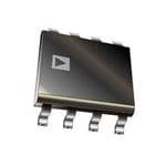
| 描述 | IC OPAMP INSTR 800KHZ 8SOIC仪表放大器 Low Drift Low Power |
| 产品分类 | Linear - Amplifiers - Instrumentation, OP Amps, Buffer Amps集成电路 - IC |
| 品牌 | Analog Devices |
| 产品手册 | |
| 产品图片 |
|
| rohs | 符合RoHS无铅 / 符合限制有害物质指令(RoHS)规范要求 |
| 产品系列 | 放大器 IC,仪表放大器,Analog Devices AD621ARZ- |
| 数据手册 | |
| 产品型号 | AD621ARZ |
| 产品培训模块 | http://www.digikey.cn/PTM/IndividualPTM.page?site=cn&lang=zhs&ptm=25193http://www.digikey.cn/PTM/IndividualPTM.page?site=cn&lang=zhs&ptm=30008http://www.digikey.cn/PTM/IndividualPTM.page?site=cn&lang=zhs&ptm=26202 |
| 产品目录页面 | |
| 产品种类 | 仪表放大器 |
| 供应商器件封装 | 8-SOIC N |
| 共模抑制比—最小值 | 110 dB |
| 关闭 | No Shutdown |
| 包装 | 管件 |
| 单电源电压 | - |
| 压摆率 | 1.2 V/µs |
| 双重电源电压 | 2.3 V to 18 V |
| 可用增益调整 | 100 V/V |
| 商标 | Analog Devices |
| 增益带宽生成 | - |
| 增益带宽积 | - |
| 安装类型 | 表面贴装 |
| 安装风格 | SMD/SMT |
| 封装 | Tube |
| 封装/外壳 | 8-SOIC(0.154",3.90mm 宽) |
| 封装/箱体 | SOIC-8 |
| 工作温度 | -40°C ~ 85°C |
| 工作温度范围 | - 40 C to + 85 C |
| 工作电源电压 | 2.3 V to 18 V |
| 工厂包装数量 | 98 |
| 带宽 | 800 kHz |
| 放大器类型 | Instumentation Amplifier |
| 最大功率耗散 | 650 mW |
| 最大工作温度 | + 85 C |
| 最大输入电阻 | 10 GOhms at +/- 15 V |
| 最小工作温度 | - 40 C |
| 标准包装 | 98 |
| 电压-电源,单/双 (±) | ±2.3 V ~ 18 V |
| 电压-输入失调 | 75µV |
| 电流-电源 | 900µA |
| 电流-输入偏置 | 500pA |
| 电流-输出/通道 | 18mA |
| 电源电流 | 0.9 mA |
| 电路数 | 1 |
| 系列 | AD621 |
| 视频文件 | http://www.digikey.cn/classic/video.aspx?PlayerID=1364138032001&width=640&height=505&videoID=2245193153001http://www.digikey.cn/classic/video.aspx?PlayerID=1364138032001&width=640&height=505&videoID=2245193159001 |
| 转换速度 | 1.2 V/us |
| 输入偏压电流—最大 | 2 nA |
| 输入补偿电压 | 35 uV |
| 输出电流 | 18 mA |
| 输出类型 | - |
| 通道数量 | 1 Channel |


- 商务部:美国ITC正式对集成电路等产品启动337调查
- 曝三星4nm工艺存在良率问题 高通将骁龙8 Gen1或转产台积电
- 太阳诱电将投资9.5亿元在常州建新厂生产MLCC 预计2023年完工
- 英特尔发布欧洲新工厂建设计划 深化IDM 2.0 战略
- 台积电先进制程称霸业界 有大客户加持明年业绩稳了
- 达到5530亿美元!SIA预计今年全球半导体销售额将创下新高
- 英特尔拟将自动驾驶子公司Mobileye上市 估值或超500亿美元
- 三星加码芯片和SET,合并消费电子和移动部门,撤换高东真等 CEO
- 三星电子宣布重大人事变动 还合并消费电子和移动部门
- 海关总署:前11个月进口集成电路产品价值2.52万亿元 增长14.8%


PDF Datasheet 数据手册内容提取
a Low Drift, Low Power Instrumentation Amplifier AD621 FEATURES CONNECTION DIAGRAM EASY TO USE 8-Lead Plastic Mini-DIP (N), Cerdip (Q) Pin-Strappable Gains of 10 and 100 and SOIC (R) Packages All Errors Specified for Total System Performance Higher Performance than Discrete In Amp Designs Available in 8-Lead DIP and SOIC G = 10/100 1 8 G = 10/100 Low Power, 1.3 mA Max Supply Current –IN 2 AD621 7 +VS Wide Power Supply Range ((cid:1)2.3 V to (cid:1)18 V) +IN 3 (NToOt Pto V SIEcWale) 6 OUTPUT EXCELLENT DC PERFORMANCE –VS 4 5 REF 0.15% Max, Total Gain Error (cid:1)5 ppm/(cid:2)C, Total Gain Drift gain drift errors are achieved by the use of internal gain setting 125 (cid:3)V Max, Total Offset Voltage resistors. Fixed gains of 10 and 100 can easily be set via external 1.0 (cid:3)V/(cid:2)C Max, Offset Voltage Drift pin strapping. The AD621 is fully specified as a total system, therefore, simplifying the design process. LOW NOISE 9 nV/√Hz, @ 1 kHz, Input Voltage Noise For portable or remote applications, where power dissipation, 0.28 (cid:3)V p-p Noise (0.1 Hz to 10 Hz) size, and weight are critical, the AD621 features a very low EXCELLENT AC SPECIFICATIONS supply current of 1.3 mA max and is packaged in a compact 800 kHz Bandwidth (G = 10), 200 kHz (G = 100) 8-lead SOIC, 8-lead plastic DIP or 8-lead cerdip. The AD621 12 (cid:3)s Settling Time to 0.01% also excels in applications requiring high total accuracy, such as precision data acquisition systems used in weigh scales and APPLICATIONS transducer interface circuits. Low maximum error specifications Weigh Scales including nonlinearity of 10 ppm, gain drift of 5 ppm/°C, 50 µV Transducer Interface and Data Acquisition Systems offset voltage, and 0.6 µV/°C offset drift (“B” grade), make Industrial Process Controls possible total system performance at a lower cost than has been Battery-Powered and Portable Equipment previously achieved with discrete designs or with other mono- PRODUCT DESCRIPTION lithic instrumentation amplifiers. The AD621 is an easy to use, low cost, low power, high accu- When operating from high source impedances, as in ECG and racy instrumentation amplifier that is ideally suited for a wide blood pressure monitors, the AD621 features the ideal combina- range of applications. Its unique combination of high perfor- tion of low noise and low input bias currents. Voltage noise is mance, small size and low power, outperforms discrete in amp specified as 9 nV/√Hz at 1 kHz and 0.28 µV p-p from 0.1 Hz to implementations. High functionality, low gain errors, and low 10 Hz. Input current noise is also extremely low at 0.1 pA/√Hz. 30,000 The AD621 outperforms FET input devices with an input bias current specification of 1.5 nA max over the full industrial tem- LE 25,000 perature range. A L SC I3N O APM APMP p 10,000 ppm OF FUL 2105,,000000 (3 OP 07S) (cid:3)= 100 – Vp- 1,000 TOTAL ERROR, 150,,000000 AD621A LTAGE NOISE, G (0.1 – 10Hz) 11000 TBINYIP PAOIMCLPAALR SINTPAUNTDARD VO AD621 SUPER(cid:5)ETA 0 T BIPOLAR INPUT 0 5 10 15 20 U IN AMP SUPPLY CURRENT – mA NP 1 L I A Figure 1.Three Op Amp IA Designs vs. AD621 T O T 0.1 1k 10k 100k 1M 10M 100M SOURCE RESISTANCE – (cid:4) REV.B Figure 2.Total Voltage Noise vs. Source Resistance Information furnished by Analog Devices is believed to be accurate and reliable. However, no responsibility is assumed by Analog Devices for its use, nor for any infringements of patents or other rights of third parties One Technology Way, P.O. Box 9106, Norwood, MA 02062-9106, U.S.A. which may result from its use. No license is granted by implication or Tel: 781/329-4700 World Wide Web Site: http://www.analog.com otherwise under any patent or patent rights of Analog Devices. Fax: 781/326-8703 © Analog Devices, Inc., 2001
AD621–SPECIFICATIONS Gain = 10 (Typical @ 25(cid:2)C, V = (cid:1)15V, and R = 2 k(cid:4), unless otherwise noted.) S L AD621A AD621B AD621S1 Model Conditions Min Typ Max Min Typ Max Min Typ Max Unit GAIN Gain Error V = ±10 V 0.15 0.05 0.15 % OUT Nonlinearity, V = –10 V to +10 V R = 2 kΩ 2 10 2 10 2 10 ppm of FS OUT L Gain vs. Temperature –1.5 ±5 –1.5 ±5 –1 ±5 ppm/°C TOTAL VOLTAGE OFFSET Offset (RTI) V = ±15 V 75 250 50 125 75 250 µV S Over Temperature V = ±5 V to ±15 V 400 215 500 µV S Average TC V = ±5 V to ±15 V 1.0 2.5 0.6 1.5 1.0 2.5 µV/°C S Offset Referred to the Input vs. Supply (PSR)2 V = ±2.3 V to ±18 V 95 120 100 120 95 120 dB S Total NOISE Voltage Noise (RTI) 1 kHz 13 17 13 17 13 17 nV/√Hz RTI 0.1 Hz to 10 Hz 0.55 0.55 0.8 0.55 0.8 µV p-p Current Noise f = 1 kHz 100 100 100 fA/√Hz 0.1 Hz–10 Hz 10 10 10 pA p-p INPUT CURRENT V = ±15 V S Input Bias Current 0.5 2.0 0.5 1.0 0.5 2 nA Over Temperature 2.5 1.5 4 nA Average TC 3.0 3.0 8.0 pA/°C Input Offset Current 0.3 1.0 0.3 0.5 0.3 1.0 nA Over Temperature 1.5 0.75 2.0 nA Average TC 1.5 1.5 8.0 pA/°C INPUT Input Impedance Differential 10(cid:1)2 10(cid:1)2 10(cid:1)2 GΩ(cid:1)pF Common-Mode 10(cid:1)2 10(cid:1)2 10(cid:1)2 GΩ(cid:1)pF Input Voltage Range3 V = ±2.3 V to ±5 V –V + 1.9 +V – 1.2 –V + 1.9 +V – 1.2 –V + 1.9 +V – 1.2 V S S S S S S S Over Temperature –V + 2.1 +V – 1.3 –V + 2.1 +V – 1.3 –V + 2.1 +V – 1.3 V S S S S S S V = ±5 V to ±18 V –V + 1.9 +V – 1.4 –V + 1.9 +V – 1.4 –V + 1.9 +V – 1.4 V S S S S S S S Over Temperature –V + 2.1 +V – 1.4 –V + 2.1 +V – 1.4 –V + 2.3 +V – 1.4 V S S S S S S Common-Mode Rejection Ratio DC to 60 Hz with 1 kΩ Source Imbalance V = 0 V to ±10 V 93 110 100 110 93 110 dB CM OUTPUT Output Swing R = 10 kΩ, L V = ±2.3 V to ±5 V –V + 1.1 +V – 1.2 –V + 1.1 +V – 1.2 –V + 1.1 +V – 1.2 V S S S S S S S Over Temperature –V + 1.4 +V – 1.3 –V + 1.4 +V – 1.3 –V + 1.6 +V – 1.3 V S S S S S S V = ±5 V to ±18 V –V + 1.2 +V – 1.4 –V + 1.2 +V – 1.4 –V + 1.2 +V – 1.4 V S S S S S S S Over Temperature –V + 1.6 +V – 1.5 –V + 1.6 +V – 1.5 –V + 2.3 +V – 1.5 V S S S S S S Short Current Circuit ±18 ±18 ±18 mA DYNAMIC RESPONSE Small Signal, –3 dB Bandwidth 800 800 800 kHz Slew Rate 0.75 1.2 0.75 1.2 0.75 1.2 V/µs Settling Time to 0.01% 10 V Step 12 12 12 µs REFERENCE INPUT R 20 20 20 kΩ IN I V +, V = 0 50 60 50 60 +50 +60 µA IN IN REF Voltage Range –V + 1.6 +V – 1.6 –V + 1.6 +V – 1.6 V + 1.6 +V – 1.6 V S S S S S S Gain to Output 1 ± 0.0001 1 ± 0.0001 1 ± 0.0001 POWER SUPPLY Operating Range ±2.3 ±18 ±2.3 ±18 ±2.3 ±18 V Quiescent Current V = ±2.3 V to ±18 V 0.9 1.3 0.9 1.3 0.9 1.3 mA S Over Temperature 1.1 1.6 1.1 1.6 1.1 1.6 mA TEMPERATURE RANGE For Specified Performance –40 to +85 –40 to +85 –55 to +125 °C NOTES 1See Analog Devices’ military data sheet for 883B tested specifications. 2This is defined as the supply range over which PSRR is defined. 3Input Voltage Range = CMV + (Gain × V ). DIFF Specifications subject to change without notice. –2– REV. B
AD621 Gain = 100 (Typical @ 25(cid:2)C, V = (cid:1)15V, and R = 2 k(cid:4), unless otherwise noted.) S L AD621A AD621B AD621S1 Model Conditions Min Typ Max Min Typ Max Min Typ Max Unit GAIN Gain Error V = ±10 V 0.15 0.05 0.15 % OUT Nonlinearity, V = –10 V to +10 V R = 2 kΩ 2 10 2 10 2 10 ppm of FS OUT L Gain vs. Temperature –1 ±5 –1 ±5 –1 ±5 ppm/°C TOTAL VOLTAGE OFFSET Offset (RTI) V = ±15 V 35 125 25 50 35 125 µV S Over Temperature V = ±5 V to ±15 V 185 215 225 µV S Average TC V = ±5 V to ±15 V 0.3 1.0 0.1 0.6 0.3 1.0 µV/°C S Offset Referred to the Input vs. Supply (PSR)2 V = ±2.3 V to ±18 V 110 140 120 140 110 140 dB S Total NOISE Voltage Noise (RTI) 1 kHz 9 13 9 13 9 13 nV/√Hz RTI 0.1 Hz to 10 Hz 0.28 0.28 0.4 0.28 0.4 µV p-p Current Noise f = 1 kHz 100 100 100 fA/√Hz 0.1 Hz–10 Hz 10 10 10 pA p-p INPUT CURRENT V = ±15 V S Input Bias Current 0.5 2.0 0.5 1.0 0.5 2 nA Over Temperature 2.5 1.5 4 nA Average TC 3.0 3.0 8.0 pA/°C Input Offset Current 0.3 1.0 0.3 0.5 0.3 1.0 nA Over Temperature 1.5 0.75 2.0 nA Average TC 1.5 1.5 8.0 pA/°C INPUT Input Impedance Differential 10(cid:1)2 10(cid:1)2 10(cid:1)2 GΩ(cid:1)pF Common-Mode 10(cid:1)2 10(cid:1)2 10(cid:1)2 GΩ(cid:1)pF Input Voltage Range3 V = ±2.3 V to ±5 V –V + 1.9 +V – 1.2 –V + 1.9 +V – 1.2 –V + 1.9 +V – 1.2 V S S S S S S S Over Temperature –V + 2.1 +V – 1.3 –V + 2.1 +V – 1.3 –V + 2.1 +V – 1.3 V S S S S S S V = ±5 V to ±18 V –V + 1.9 +V – 1.4 –V + 1.9 +V – 1.4 –V + 1.9 +V – 1.4 V S S S S S S S Over Temperature –V + 2.1 +V – 1.4 –V + 2.1 +V – 1.4 –V + 2.3 +V – 1.4 V S S S S S S Common-Mode Rejection Ratio DC to 60 Hz with 1 kΩ Source Imbalance V = 0 V to ±10 V 110 130 120 130 110 130 dB CM OUTPUT Output Swing R = 10 kΩ, L V = ±2.3 V to ±5 V –V + 1.1 +V – 1.2 –V + 1.1 +V – 1.2 –V + 1.1 +V – 1.2 V S S S S S S S Over Temperature –V + 1.4 +V – 1.3 –V + 1.4 +V – 1.3 –V + 1.6 +V – 1.3 V S S S S S S V = ±5 V to ±18 V –V + 1.2 +V – 1.4 –V + 1.2 +V – 1.4 –V + 1.2 +V – 1.4 V S S S S S S S Over Temperature –V + 1.6 +V – 1.5 –V + 1.6 +V – 1.5 –V + 2.3 +V – 1.5 V S S S S S S Short Current Circuit ±18 ±18 ±18 mA DYNAMIC RESPONSE Small Signal, –3 dB Bandwidth 200 200 200 kHz Slew Rate 0.75 1.2 0.75 1.2 0.75 1.2 V/µs Settling Time to 0.01% 10 V Step 12 12 12 µs REFERENCE INPUT R 20 20 20 kΩ IN I V +, V = 0 50 60 50 60 50 60 µA IN IN REF Voltage Range –V + 1.6 +V – 1.6 –V + 1.6 +V – 1.6 V + 1.6 +V – 1.6 V S S S S S S Gain to Output 1 ± 0.0001 1 ± 0.0001 1 ± 0.0001 POWER SUPPLY Operating Range ±2.3 ±18 ±2.3 ±18 ±2.3 ±18 V Quiescent Current V = ±2.3 V to ±18 V 0.9 1.3 0.9 1.3 0.9 1.3 mA S Over Temperature 1.1 1.6 1.1 1.6 1.1 1.6 mA TEMPERATURE RANGE For Specified Performance –40 to +85 –40 to +85 –55 to +125 °C NOTES 1See Analog Devices’ military data sheet for 883B tested specifications. 2This is defined as the supply range over which PSEE is defined. 3Input Voltage Range = CMV + (Gain × V ). DIFF Specifications subject to change without notice. REV. B –3–
AD621 ABSOLUTE MAXIMUM RATINGS1 ESD SUSCEPTIBILITY SupplyVoltage . . . . . . . . . . . . . . . . . . . . . . . . . . . . . . . . ±18V ESD (electrostatic discharge) sensitive device. Electrostatic InternalPowerDissipation2 . . . . . . . . . . . . . . . . . . . . 650 mW charges as high as 4000 volts, which readily accumulate on the Input Voltage (Common Mode) . . . . . . . . . . . . . . . . . . . . ±V human body and on test equipment, can discharge without S DifferentialInputVoltage . . . . . . . . . . . . . . . . . . . . . . . ±25V detection. Although the AD621 features proprietary ESD pro- Output Short Circuit Duration . . . . . . . . . . . . . . . . Indefinite tection circuitry, permanent damage may still occur on these Storage Temperature Range (Q) . . . . . . . . . –65°C to +150°C devices if they are subjected to high energy electrostatic dis- Storage Temperature Range (N, R) . . . . . . . –65°C to +125°C charges. Therefore, proper ESD precautions are recommended Operating Temperature Range to avoid any performance degradation or loss of functionality. AD621 (A, B) . . . . . . . . . . . . . . . . . . . . . . –40°C to +85°C AD621 (S) . . . . . . . . . . . . . . . . . . . . . . . . –55°C to +125°C ORDERING GUIDE Lead Temperature Range (Soldering10seconds) . . . . . . . . . . . . . . . . . . . . . . . . 300°C Temperature Package Package Model Range Description Option1 NOTES 1Stresses above those listed under Absolute Maximum Ratings may cause perma- AD621AN –40°C to +85°C 8-Lead Plastic DIP N-8 nent damage to the device. This is a stress rating only; functional operation of the AD621BN –40°C to +85°C 8-Lead Plastic DIP N-8 device at these or any other conditions above those indicated in the operational AD621AR –40°C to +85°C 8-Lead Plastic SOIC R-8 section of this specification is not implied. Exposure to absolute maximum rating AD621BR –40°C to +85°C 8-Lead Plastic SOIC R-8 conditions for extended periods may affect device reliability. AD621SQ/883B2 –55°C to +125°C 8-Lead Cerdip Q-8 2Specification is for device in free air: 8-Lead Plastic Package: θ = 95°C/W AD621ACHIPS –40°C to +85°C Die JA 8-Lead Cerdip Package: θ = 110°C/W 8-Lead SOIC Package: θ J A= 155°C/W NOTES JA 1N = Plastic DIP; Q = Cerdip; R = SOIC. 2See Analog Devices’ military data sheet for 883B specifications. METALIZATION PHOTOGRAPH Dimensions shown in inches and (mm). Contact factory for latest dimensions. 1.125 (3.57) +VS OUTPUT 7 6 RG 8 5 REFERENCE 0.0708 (2.545) RG 1 4 –VS 2 3 –IN +IN –4– REV. B
Typical Performance Characteristics–AD621 50 50 SAMPLE SIZE = 90 SAMPLE SIZE = 90 40 40 S S NIT NIT U U F 30 F 30 O O E E G G A A CENT 20 CENT 20 R R E E P P 10 10 0 0 –200 –100 0 +100 +200 –800 –400 0 +400 +800 INPUT OFFSET VOLTAGE – (cid:3)V INPUT BIAS CURRENT – pA TPC 1.Typical Distribution of V Gain = 10 TPC 4.Typical Distribution of Input Bias Current OS, 50 2.0 SAMPLE SIZE = 90 V 40 (cid:3)– F UNITS 30 OLTAGE 1.5 O V E T G E 1.0 CENTA 20 N OFFS ER E I P G N 0.5 10 HA C 0 0 –80 –40 0 +40 +80 0 1 2 3 4 5 INPUT OFFSET VOLTAGE – (cid:3)V WARM-UP TIME – Minutes TPC 2.Typical Distribution of V , Gain = 100 TPC 5.Change in Input Offset Voltage vs. Warm-Up Time OS 50 1000 SAMPLE SIZE = 90 40 E OF UNITS 30 SE – nV/ Hz 100 TAG NOI GAIN = 10 EN 20 GE ERC LTA 10 P O 10 V GAIN = 100 0 –400 –200 0 +200 +400 11 10 100 1k 10k 100k INPUT OFFSET CURRENT – pA FREQUENCY – Hz TPC 3.Typical Distribution of Input Offset Current TPC 6.Voltage Noise Spectral Density REV. B –5–
AD621 1000 100mV 1s V/ Hz 19000 n – E S OI 100 N T N E R R U 10 C 0% 10 1 10 100 1000 FREQUENCY – Hz TPC 7.Current Noise Spectral Density vs. Frequency TPC 9.0.1 Hz to 10 Hz Current Noise, 5 pA per Vertical Div, 1 Second per Horizontal Div 100,000 V (cid:3) – TI R (cid:3)SE – 0.2V/div (cid:2)(cid:2)M 25C TO 85C, 101,000000 FINE TA MINPPUT OI O TI N T FR R F DRI 100 L AD621A A T O T 10 TIME – 1 sec/div 1k 10k 100k 1M 10M SOURCE RESISTANCE – (cid:4) TPC 8a.0.1 Hz to 10 Hz RTI Voltage Noise, Gain = 10 TPC 10.Total Drift vs. Source Resistance 160 140 GAIN = 100 120 v di (cid:3)V/ 100 GAIN = 10 0.1 dB E – R – 80 S M OI C N 60 TI R 40 20 0 TIME – 1 sec/div 0.1 1 10 100 1k 10k 100k 1M FREQUENCY – Hz TPC 8b.0.1 Hz to 10 Hz RTI Voltage Noise, G = 100 TPC 11.CMR vs. Frequency, RTI, for a Zero to 1 kΩ Source Imbalance –6– REV. B
AD621 180 35 G = 10 & 100 160 30 G = 100 p 140 p- s 25 120 Volt dB G = 10 E – 20 PSR – 100 OLTAG15 80 V T U P10 60 T U O 40 5 20 0 0.1 1 10 100 1k 10k 100k 1M 1k 10k 100k 1M FREQUENCY – Hz FREQUENCY – Hz TPC 12.Positive PSR vs. Frequency TPC 15.Large Signal Frequency Response 180 +VS –0.0 160 –0.5 G = 100 ES) 114200 T – VoltsVOLTAG ––11..50 B G = 10 MIY R – d100 GE LIUPPL S AS P 80 VOLTD TO +1.5 60 INPUT EFERRE +1.0 40 (R +0.5 200.1 1 10 100 1k 10k 100k 1M –VS +0.00 5 10 15 20 FREQUENCY – Hz SUPPLY VOLTAGE (cid:1) Volts TPC 13.Negative PSR vs. Frequency TPC 16.Input Voltage Range vs. Supply Voltage 1000 +VS –0.0 S) –0.5 RL = 10k(cid:4) E SED-LOOP GAIN – V/V 11000 VOLTAGE LIMIT – VoltsD TO SUPPLY VOLTAG +––111...550 RLR =L =2 k2(cid:4)k(cid:4) CLO 1 INPUT EFERRE +1.0 (R +0.5 RL = 10k(cid:4) 0.1 –VS +0.0 100 1k 10k 100k 1M 10M 0 5 10 15 20 FREQUENCY – Hz SUPPLY VOLTAGE (cid:1) Volts TPC 14.Closed-Loop Gain vs. Frequency TPC 17.Output Voltage Swing vs. Supply Voltage, G = 10 REV. B –7–
AD621 30 p p- 5V 1mV 10(cid:3)s olts VGS = = 1 (cid:1)0 15V – V 20 100 G 90 N WI S E G A T L O 10 V T U P 10 T U 0% O 0 0 100 1k 10k LOAD RESISTANCE – (cid:4) TPC 18.Output Voltage Swing vs. Resistive Load TPC 21.Large Signal Pulse Response and Settling Time, G = 100 (0.5 mV = 0.1%), R = 2 kΩ, C = 100 pF L L 5V 1mV 10(cid:3)s 20mV 10(cid:3)s 100 100 90 90 10 10 0% 0% TPC 19.Large Signal Pulse Response and Settling TPC 22.Small Signal Pulse Response, G = 100, Time Gain, G = 10 (0.5 mV = 0.01%), R = 1 kΩ, R = 2 kΩ, C = 100 pF L L L C = 100 pF L 20 20mV 10(cid:3)s TO 0.01% 100 15 90 s (cid:3) – E M TO 0.1% G TI 10 N LI T T E S 10 5 0% 0 0 5 10 15 20 OUTPUT STEP SIZE – Volts TPC 20.Small Signal Pulse Response, G = 10, TPC 23.Settling Time vs. Step Size, G = 10 R = 1 kΩ, C = 100 pF L L –8– REV. B
AD621 20 100(cid:3)V 2V TO 0.01% 15 100 90 s (cid:3) – ME TO 0.1% G TI10 N LI T T E S 10 5 0% 0 0 5 10 15 20 OUTPUT STEP SIZE – Volts TPC 24.Settling Time vs. Step Size, Gain = 100 TPC 27.Gain Nonlinearity, G = 10, R = 10 kΩ, Vertical L Scale: 100 µV/Div = 100 ppm/Div, Horizontal Scale: 2 Volts/Div 2.0 10k(cid:4) 1k(cid:4) 10k(cid:4) 1.5 1% 10T 1% +IB nA 1.0 100k(cid:4) +VS VOUT RRENT – 0.50 –IB 20INVP pU-Tp G = 11%0 G = 100 – U G = 10 UT C–0.5 101.k1(cid:4)% 10k.1(cid:4)% G = 100 AD621 P N I–1.0 + –1.5 –VS –2.0 –125 –75 –25 25 75 125 175 TEMPERATURE – (cid:2)C TPC 25.Input Bias Current vs. Temperature TPC 28.Settling Time Test Circuit 0PW 0 VZR 0 100(cid:3)V 2V 100 90 10 0% 0 WFM 20 WFM AQR WARNING TPC 26.Gain Nonlinearity, G = 100, R = 10 kΩ, L C = 0 pF. Vertical Scale: 100 µV/Div = 100 ppm/Div L Horizontal Scale: 2 Volts/Div REV. B –9–
AD621 +VS R5 at a gain of 10 or the parallel combination of R5 and R6 at a 7 gain of 100. I1 20(cid:3)A VB 20(cid:3)A I2 This creates a differential gain from the inputs to the A1/A2 outputs given by G = (R1 + R2) / RG + 1. The unity-gain – + + – subtracter A3 removes any common-mode signal, yielding a A1 A2 10k(cid:4) single-ended output referred to the REF pin potential. C1 C2 10k(cid:4) The value of RG also determines the transconductance of the – OUTPUT A3 preamp stage. As RG is reduced for larger gains, the transcon- + 6 40R03(cid:4) R1 25k(cid:4)R5 R2 25k(cid:4) 10k(cid:4) 10k(cid:4) REF dTuhcitsa hncaes itnhcrreeea siems paosyrmtapntto taidcavlalyn ttoag tehsa:t (oaf) t hOep iennp-ulto torpan gsaisitno riss. –IN Q1 5555.6(cid:4) Q2 +IN 5 boosted for increasing programmed gain, thus reducing gain- 2 R4 3 R6 400(cid:4) related errors. (b) The gain-bandwidth product (determined by 555.6(cid:4) C1, C2 and the preamp transconductance) increases with pro- 1 8 G = 100 G = 100 grammed gain, thus optimizing frequency response. (c) The input voltage noise is reduced to a value of 9 nV/√Hz, deter- 4 mined mainly by the collector current and base resistance of the –VS input devices. Figure 3.Simplified Schematic of AD621 Make vs. Buy: A Typical Bridge Application Error Budget The AD621 offers improved performance over discrete three op THEORY OF OPERATION amp IA designs, along with smaller size, fewer components and The AD621 is a monolithic instrumentation amplifier based on 10 times lower supply current. In the typical application, shown a modification of the classic three op amp circuit. Careful layout in Figure 4, a gain of 100 is required to amplify a bridge output of of the chip, with particular attention to thermal symmetry builds 20 mV full scale over the industrial temperature range of –40°C to in tight matching and tracking of critical components, thus +85°C. The error budget table below shows how to calculate preserving the high level of performance inherent in this circuit, the effect various error sources have on circuit accuracy. at a low price. Regardless of the system it is being used in, the AD621 provides On chip gain resistors are pretrimmed for gains of 10 and 100. greater accuracy, and at low power and price. In simple systems, The AD621 is preset to a gain of 10. A single external jumper absolute accuracy and drift errors are by far the most significant (between Pins 1 and 8) is all that is needed to select a gain of contributors to error. In more complex systems with an intelligent 100. Special design techniques assure a low gain TC of 5 ppm/°C processor, an autogain/autozero cycle will remove all absolute max, even at a gain of 100. accuracy and drift errors leaving only the resolution errors of gain nonlinearity and noise, thus allowing full 14-bit accuracy. Figure 3 is a simplified schematic of the AD621. The input transistors Q1 and Q2 provide a single differential-pair bipolar Note that for the discrete circuit, the OP07 specifications for input for high precision, yet offer 10× lower Input Bias Current, input voltage offset and noise have been multiplied by 2. This is thanks to Superβeta processing. Feedback through the Q1-A1-R1 because a three op amp type in amp has two op amps at its inputs, loop and the Q2-A2-R2 loop maintains constant collector cur- both contributing to the overall input error. rent of the input devices Q1 and Q2, thereby impressing the input voltage across the gain-setting resistor, RG, which equals 10V + 10k(cid:4)* 10k(cid:4)* OP07D – R = 350(cid:4) R = 350(cid:4) + 10k(cid:4)** – AD621A 100k(cid:4)** OP07D – + REFERENCE 10k(cid:4)** R = 350(cid:4) R = 350(cid:4) – OP07D + 10k(cid:4)* 10k(cid:4)* AD621A MONOLITHIC INSTRUMENTATION AMPLIFIER, G = 100 3 OP AMP, IN AMP, G = 100 * 0.02% RESISTOR MATCH, 3PPM/(cid:2)C TRACKING PRECISION BRIDGE TRANSDUCER SUPPLY CURRENT = 1.3mA MAX ** DISCRETE 1% RESISTOR, 100PPM/(cid:2)C TRACKING SUPPLY CURRENT = 15mA MAX Figure 4.Make vs. Buy –10– REV. B
AD621 5V 20k(cid:4) + 3k(cid:4) 3k(cid:4) REF AD621B IN 3k(cid:4) 3k(cid:4) DIGITAL 10k(cid:4) ADC DATA – OUTPUT + 20k(cid:4) AD705 AGND – 1.7mA 1.3mA 0.10mA 0.6mA MAX MAX Figure 5.A Pressure Monitor Circuit which Operates on a 5 V Power Supply Pressure Measurement presence of large, unwanted common-mode signals or offsets. Although useful in many bridge applications such as weigh-scales, Many monolithic in amps achieve low total input drift and noise the AD621 is especially suited for higher resistance pressure errors only at relatively high gains (~100). In contrast the AD621’s sensors powered at lower voltages where small size and low low output errors allow such performance at a gain of 10, thus power become more even significant. allowing larger input signals and therefore greater dynamic Figure 5 shows a 3 kΩ pressure transducer bridge powered from range. The circuit of Figure 6 (±15 V supply, G = 10) has only 2.5 µV/°C max. V drift and 0.55 µ/V p-p typical 0.1 Hz 5 V. In such a circuit, the bridge consumes only 1.7 mA. Adding OS to 10 Hz noise, yet will amplify a ±0.5 V differential signal while the AD621 and a buffered voltage divider allows the signal to be suppressing a ±10 V common-mode signal, or it will amplify a conditioned for only 3.8 mA of total supply current. ±1.25 V differential signal while suppressing a 1 V offset by use Small size and low cost make the AD621 especially attractive for of the DAC driving the reference pin of the AD621. An added voltage output pressure transducers. Since it delivers low noise benefit, the offsetting DAC connected to the reference pin allows and drift, it will also serve applications such as diagnostic non- removal of a dc signal without the associated time-constant invasion blood pressure measurement. of ac coupling. Note the representations of a differential and Wide Dynamic Range Gain Block Suppresses Large Common- common-mode signal shown in Figure 6 such that a single-ended Mode and Offset Signals (or normal mode) signal of 1 V would be composed of a 0.5 V The AD621 is especially useful in wide dynamic range applica- common-mode component and a 1 V differential component. tions such as those requiring the amplification of signals in the Table I. Make vs. Buy Error Budget AD621 Circuit Discrete Circuit Error, ppm of Full Scale Error Source Calculation Calculation AD621 Discrete ABSOLUTE ACCURACY at T = +25°C A Input Offset Voltage, µV 125 µV/20 mV (150 µV × 2/20 mV 16,250 15,000 Output Offset Voltage, µV N/A ((150 µV × 2)/100)/20 mV N/A 12,150 Input Offset Current, nA 2 nA × 350 Ω/20 mV (6 nA × 350 Ω)/20 mV 12,118 121,53 CMR, dB 110 dB→3.16 ppm, × 5 V/20 mV (0.02% Match × 5 V)/20 mV 12,791 14,988 Total Absolute Error 17,558 20,191 DRIFT TO +85°C Gain Drift, ppm/°C 5 ppm × 60°C 100 ppm/°C Track × 60°C 13,300 12,600 Input Offset Voltage Drift, µV/°C 1µV/°C × 60°C/20 mV (2.5µV/°C × 2 × 60°C)/20 mV 13,000 15,000 Output Offset Voltage Drift, µV/°C N/A (2.5 µV/°C × 2 × 60°C)/100/20 mV N/A 12,150 Total Drift Error 13,690 15,750 RESOLUTION Gain Nonlinearity, ppm of Full Scale 40 ppm 40 ppm 12,140 12,140 Typ 0.1 Hz–10 Hz Voltage Noise, µV p-p 0.28 µV p-p/20 mV (0.38 µV p-p × √2)120 mV 121,14 12,127 Total Resolution Error 121,54 121,67 Grand Total Error 11,472 36,008 G = 100, V = ±15 V. S (All errors are min/max and referred to input.) REV. B –11–
AD621 INPUT A: + (cid:1)10V CM VDIFF (cid:1)0.5V – + VCOM OPTIONAL (cid:1)10V– – (cid:6)10 VOUT1 10k(cid:4) – AD621 G = 10 (cid:6)10 VOUT2 + DAC AD621 TOTAL GAIN = 100 INPUT B: 0 TO (cid:1)10V (cid:1)1V + 10k(cid:4) + OFFSET VDIFF + VOFFSET (cid:1)(1.25V + 1V) – USE THIS IN PLACE OF THE DAC FOR ZERO SUPPRESSION FUNCTION. TO TO REF C VOUT1 R – AD548 + Figure 6.Suppressing a Large Common-Mode or Offset Voltage in Order to Measure a Small Differential Signal (V = ±15 V) S The AD621, as well as many other monolithic instrumentation The AD621’s input amplifiers can provide output voltage within amplifiers, is based on the “three op amp” in amp circuit (Fig- 2.5 V of the supplies. To avoid saturation of the input amplifier ure 7) amplifier. Since the input amplifiers (A1 and A2) have a the input voltage must therefore obey the equations: common-mode gain of unity and a differential gain equal to the V + G × V /2 ≤ (Upper Supply – 2.5 V) set gain of the overall in amp, the voltages V1 and V2 are defined CM DIFF V – G × V /2 ≥ (Lower Supply + 2.5 V) by the equations CM DIFF V = V + G × V /2 Figure 8 shows the trade-off between common-mode and 1 CM DIFF differential-mode input for ±15 V supplies and G = 10. V = V – G × V /2 2 CM DIFF By cascading with use of the optional AD621, the circuit of The common-mode voltage will drive the outputs of amplifiers Figure 6 will provide ±1 V of zero suppression at gains of 10 A1 and A2 to the differential-signal voltage, multiplied by the and 100 (at V and V respectively) with maximum TCs gain, spreads them apart. For a 10 V common-mode 0.1 V of ±4 ppm/°CO aUnTd1 ±8 ppmOU/T°C2, respectively. Therefore, depend- differential input, V1 would be at 10.5 V and V2 at 9.5 V. ing on the magnitude of the differential input signal, either V or V may be used as the output. INPUT AMPLIFIER OUTPUT AMPLIFIER OUT1 OUT2 DIFFERENTIAL GAIN = 10 DIFFERENTIAL GAIN = 1 COMMON MODE GAIN = 1 COMMON MODE GAIN = 1/1000 1.2 + V1 10k(cid:4) –A1 10k(cid:4) 1.0 20k(cid:4) 4.44k(cid:4) –A3 Volts 0.8 + (cid:1) 20k(cid:4) – F0.6 – 10k(cid:4) DIF A2 V + V2 10k(cid:4) 0.4 Figure 7.Typical Three Op Amp Instrumentation 0.2 Amplifier, Differential Gain = 10 0 0 2 4 6 8 10 12 VCM – (cid:1)Volts Figure 8. Trade-Off Between V and V Range (V = CM DIFF S ±15 V, G = 10), for Reference Pin at Ground –12– REV. B
AD621 Precision V-I Converter INPUT OVERLOAD CONSIDERATIONS The AD621 along with another op amp and two resistors make Failure of a transducer, faults on input lines, or power supply a precision current source (Figure 9). The op amp buffers the sequencing can subject the inputs of an instrumentation ampli- reference terminal to maintain good CMR. The output voltage fier to voltages well beyond their linear range, or even the supply V of the AD621 appears across R1 which converts it to a cur- voltage, so it is essential that the amplifier handle these over- X rent. This current less only the input bias current of the op amp loads without being damaged. then flows out to the load. The AD621 will safely withstand continuous input overloads of ±3.0 volts (±6.0 mA). This is true for gains of 10 and 100, with +VS power on or off. The inputs of the AD621 are protected by high current capacity VIN+ +RV1X– dielectrically isolated 400 Ω thin-film resistors R3 and R4 (Fig- AD621 ure 3) and by diodes which protect the input transistors Q1 and VIN– Q2 from reverse breakdown. If reverse breakdown occurred, there IL would be a permanent increase in the amplifier’s input current. –VS AD705 The input overload capability of the AD621 can be easily increased while only slightly degrading the noise, common-mode rejection IL = RV1X = (VIN+) –R (1VIN–) G LOAD and offset drift of the device by adding external resistors in series with the amplifier’s inputs as shown in Figure 10. Table II summarizes the overload voltages and total input Figure 9. Precision Voltage to Current Converter noise for a range of range of r values. Note that a 2 kΩ resis- (Operates on 1.8 mA, ±3 V) tor in series with each input will protect the AD621 from a ±15 volt continuous overload, while only increasing input noise INPUT AND OUTPUT OFFSET VOLTAGE to 13 nV√Hz—about the same level as would be expected from The AD621 is fully specified for total input errors at gains of 10 a typical unprotected 3 op amp in amp. and 100. That is, effects of all error sources within the AD621 are properly included in the guaranteed input error specs, elimi- Table II. Input Overload Protection vs. Value of Resistor R P nating the need for separate error calculation. Total Input Noise Maximum Continuous Total Error RTI = Input Error + (Output Error/G) Value of in nV√Hz @ 1 kHz Overload Voltage, V OL Total Error RTO = (Input Error × G) + Output Error Resistor R G = 10 G = 100 In Volts P 0 14 9 3 REFERENCE TERMINAL 499 Ω 14 10 6 Although usually grounded, the reference terminal may be used 1.00 kΩ 14 11 9 to offset the output of the AD621. This is useful when the load 2.00 kΩ 15 13 15 is “floating” or does not share a ground with the rest of the system. 3.01 kΩ* 16 14 21 It also provides a direct means of injecting a precise offset. 4.99 kΩ* 17 16 33 Another benefit of having a reference terminal is that it can be *1/4 watt, 1% metal-film resistor. All others are 1/8 watt, 1% RN55 quite effective in eliminating ground loops and noise in a circuit or equivalent. or system. +VS RP VOL AD621 VOUT VOL RP GAIN = 10 OR 100 –VS Figure 10.Input Overload Protection REV. B –13–
AD621 GThaein A SDel6e2c1ti ohnas accurate, low temperature coefficient (TC), +VS +VS gains of 10 and 100 available. The gain of the AD621 is nomi- 0.1(cid:3)F 0.1(cid:3)F nally set at 10; this is easily changed to a gain of 100 by simply – – connecting a jumper between Pins 1 and 8. INPUTS AD621 – + OUTPUT + AD526 + 2 G = 10 555.5(cid:4) 20k(cid:4) 0.1(cid:3)F REXT 5,555.5(cid:4) AD621 –VS 0.1(cid:3)F –VS Figure 12. A High Performance Programmable Gain Amplifier Figure 11.Programming the AD621 for Gains Between COMMON-MODE REJECTION 10 and 100 Instrumentation amplifiers like the AD621 offer high CMR As shown in Figure 11, the device can be programmed for any which is a measure of the change in output voltage when both gain between 10 and 100 by connecting a single external resistor inputs arc changed by equal amounts. These specifications are between Pins 1 and 8. Note that adding the external resistor will usually given for a full-range input voltage change and a speci- degrade both the gain accuracy and gain TC. Since the gain fied source imbalance. equation of the AD621 yields: For optimal CMR, the reference terminal should be tied to a 9(R +6,111.111) low impedance point, and differences in capacitance and resis- G =1+ (RX +555.555) tance should be kept to a minimum between the two inputs. In X many applications shielded cables are used to minimize noise, This can be solved for the nominal value of external resistor for and for best CMR over frequency the shield should he properly gains between 10 and 100: driven. Figures 13 and 14 show active data guards that are config- ured to improve ac common-mode rejections by “bootstrapping” (G–1)555.555–55,000 R = the capacitances of input cable shields, thus minimizing the X (10–G) capacitance mismatch between the inputs. Table III gives practical 1% resistor values for several com- +VS mon gains. –INPUT – 100(cid:4) AD648 Table III. Practical 1% External Resistor 100k(cid:4) Values for Gains Between 10 and 100 100k(cid:4) AD621 VOUT Desired Recommended Temperature Gain 1% Resistor Value Gain Error Coefficient (TC) 100(cid:4) –VS REFERENCE 10 ∞ (Pins 1 and 8 Open) * 5 ppm/°C max + +INPUT 20 4.42 kΩ ±10% ≈0.4 (50 ppm/°C –VS + Resistor TC) 50 698 Ω ±10% ≈0.4 (50 ppm/°C Figure 13. Differential Shield Driver, G = 10 + Resistor TC) 100 0 (Pins 1 and 8 Shorted) * 5 ppm/°C max +VS *Factory trimmed–exact value depends on grade. – INPUT 2 A High Performance Programmable Gain Amplifier 7 1 The excellent performance of the AD621 at a gain of 10 makes it a good choice to team up with the AD526 programmable gain 100(cid:4) AD548 AD621 6 VOUT amplifier (PGA) to yield a differential input PGA with gains of 8 5 10, 20, 40, 80, 160. As shown in Figure 12, the low offset of the 4 REFERENCE 3 AD621 allows total circuit offset to be trimmed using the offset + INPUT null of the AD526, with only a negligible increase in total drift –VS error. The total gain TC will be 9 ppm/°C max, with 2 µV/°C Figure 14.Common-Mode Shield Driver, G = 100 typical input offset drift. Bandwidth is 600 kHz to gains of 10 to 80, and 350 kHz at G = 160. Settling time is 13 µs to 0.01% for a 10 V output step for all gains. –14– REV. B
AD621 GROUNDING +VS Since the AD621 output voltage is developed with respect to the potential on the reference terminal, it can solve many ground- –INPUT ing problems by simply tying the REF pin to the appropriate “local ground.” AD621 VOUT In order to isolate low level analog signals from a noisy digital +INPUT LOAD environment, many data-acquisition components have separate analog and digital ground pins (Figure 15). It would be conve- –VS REFERENCE nient to use a single ground line; however, current through ground wires and PC runs of the circuit card can cause hundreds TO POWER SUPPLY GROUND of millivolts of error. Therefore, separate ground returns should be provided to minimize the current flow from the sensitive Figure 16a. Ground Returns for Bias Currents when Using points to the system ground. These ground returns must be tied Transformer Input Coupling together at some point, usually best at the ADC package as shown. +VS ANALOG P.S. DIGITAL P.S. +15V C –15V C +5V –INPUT 0.1(cid:3)F 0.1(cid:3)F AD621 VOUT 1(cid:3)F 1(cid:3)F 1(cid:3)F LOAD +INPUT 7 2 4 11 4 + –VS AD621 6 AD585 7 9 11 15 1 DIGITAL REFERENCE 3 5 6 S/H ADA5D7C4A DOAUTTAPUT TO POWER SUPPLY GROUND Figure 15.Basic Grounding Practice Figure 16b.Ground Returns for Bias Currents when Using a Thermocouple Input GROUND RETURNS FOR INPUT BIAS CURRENTS +VS Input bias currents are those currents necessary to bias the input transistors of an amplifier. There must be a direct return path –INPUT for these currents; therefore when amplifying “floating” input AD621 VOUT sources such as transformers, or ac-coupled sources, there must LOAD be a dc path from each input to ground as shown in Figures 16a +INPUT REFERENCE through 16c. Refer to the Instrumentation Amplifier Application 100k(cid:4) 100k(cid:4) Guide (free from Analog Devices) for more information regard- –VS ing in amp applications. TO POWER SUPPLY GROUND Figure 16c.Ground Returns for Bias Currents when Using AC Input Coupling REV. B –15–
AD621 OUTLINE DIMENSIONS Dimensions shown in inches and (mm). Plastic DIP (N-8) Package 8 5 0.25 0.31 (6.35) (7.87) B) 1 4 v. e 1 (r 0.3M9 A(9X.91) 0.30R E(7F.62) –1/0 0 0.035 0.01 – 0.165 0.01 (0.89 0.25) 76 (4.19 0.25) 7 0 SEATING PLANE C0 0.125 (3.18) 0.011 0.003 MIN (4.57 0.76) 0.18 0.03 0.018 0.003 0.10 (4.57 0.76) 0 - 15 (0.46 0.08) (2.54) TYP 0.033 (0.84) NOM Cerdip (Q-8) Package 0.005 (0.13) MIN 0.055 (1.4) MAX 8 5 0.310 (7.87) 0.220 (5.59) 1 4 0.070 (1.78) 0.030 (0.76) 0.320 (8.13) 0.405 (10.29) MAX 0.290 (7.37) 0.200 0.060 (1.52) (5.08) 0.015 (0.38) MAX 0.150 0.200 (5.08) (3.81) 0.015 (0.38) 0.125 (3.18) MIN 0.008 (0.20) 0.023 (0.58) 0.100 (2.54) 0 - 15 0.014 (0.36) BSC SEATING PLANE SOIC (R-8) Package 0.198 (5.03) 0.188 (4.77) 8 5 A. 0.158 (4.00) S. 0.150 (3.80) U. N 0.244 (6.200) D I 1 4 0.228 (5.80) E T N RI 0.018 (0.46) P 0.050 (1.27) 0.014 (0.36) 0.205 (5.20) TYP 0.181 (4.60) 0.094(2.39) 0.010 (0.25) 0.100 (2.59) 0.015 (0.38) 0.045 (1.15) 0.004 (0.10) 0.007 (0.18) 0.020 (0.50) –16– REV. B
Mouser Electronics Authorized Distributor Click to View Pricing, Inventory, Delivery & Lifecycle Information: A nalog Devices Inc.: AD621ANZ AD621ARZ AD621BNZ AD621BRZ AD621AR AD621AR-REEL7 AD621ARZ-R7 AD621ARZ-RL AD621BR AD621BR-REEL7 AD621BRZ-R7 AD621BRZ-RL AD621SQ/883B