ICGOO在线商城 > 集成电路(IC) > PMIC - 热管理 > AD595AQ
 Datasheet下载
- 型号: AD595AQ
- 制造商: Analog
- 库位|库存: xxxx|xxxx
- 要求:
| 数量阶梯 | 香港交货 | 国内含税 |
| +xxxx | $xxxx | ¥xxxx |
查看当月历史价格
查看今年历史价格
AD595AQ产品简介:
ICGOO电子元器件商城为您提供AD595AQ由Analog设计生产,在icgoo商城现货销售,并且可以通过原厂、代理商等渠道进行代购。 AD595AQ价格参考。AnalogAD595AQ封装/规格:PMIC - 热管理, Thermocouple Amplifier External Sensor Voltage Output 14-CDIP。您可以下载AD595AQ参考资料、Datasheet数据手册功能说明书,资料中有AD595AQ 详细功能的应用电路图电压和使用方法及教程。
AD595AQ是由Analog Devices Inc.(ADI)生产的一款PMIC(电源管理集成电路),专门用于热管理应用。该器件主要用于将热电偶信号转换为与温度成正比的模拟电压输出,广泛应用于需要精确温度测量和控制的场景。

 主要应用场景:

1. 工业自动化与控制:
   - AD595AQ在工业环境中常用于监测高温设备的温度,如炉子、锅炉、加热器等。它能够将热电偶产生的微弱信号转换为线性电压输出,便于后续电路进行处理和显示。
   - 该芯片还支持冷端补偿功能,确保在不同环境温度下依然能提供准确的温度测量结果。

2. 医疗设备:
   - 在医疗设备中,AD595AQ可用于监控患者的体温或设备的工作温度。例如,手术室中的加热设备、实验室中的恒温箱等都需要精确的温度控制,AD595AQ可以确保这些设备在安全范围内运行。
   - 医疗设备对温度精度要求较高,AD595AQ的高精度特性使其成为理想选择。

3. 航空航天与国防:
   - 在航空航天领域,AD595AQ可用于监控发动机、燃料系统和其他关键部件的温度。由于这些系统的温度范围较广且工作环境恶劣,AD595AQ的宽温度范围和可靠性使其成为理想的选择。
   - 国防应用中,AD595AQ也可用于导弹、雷达等设备的温度监测,确保其正常运行。

4. 消费电子:
   - 某些高端消费电子产品(如烤箱、咖啡机等)也使用AD595AQ来实现精确的温度控制。通过将热电偶信号转换为易于处理的电压信号,这些设备可以更精准地调节温度,提升用户体验。

5. 实验室仪器:
   - 实验室中的各种分析仪器(如色谱仪、光谱仪等)需要精确的温度控制以保证实验结果的准确性。AD595AQ可以作为温度传感器的一部分,帮助仪器保持稳定的工作温度。

 总结:
AD595AQ凭借其高精度、宽温度范围和可靠的性能,在工业、医疗、航空航天、消费电子和实验室仪器等多个领域中得到了广泛应用。它不仅简化了温度测量的设计,还提高了系统的可靠性和精度。
| 参数 | 数值 |
| 产品目录 | 集成电路 (IC)半导体 |
| 描述 | IC THERMOCOUPLE A W/COMP 14CDIP接口 - 专用 THERMOCOUPLER AMP IC |
| 产品分类 | |
| 品牌 | Analog Devices Inc |
| 产品手册 | |
| 产品图片 |
|
| rohs | 否不符合限制有害物质指令(RoHS)规范要求 |
| 产品系列 | 接口 IC,接口 - 专用,Analog Devices AD595AQ- |
| 数据手册 | |
| 产品型号 | AD595AQ |
| 产品目录页面 | |
| 产品种类 | |
| 产品类型 | IC Thermocouple Amplifier with Cold Junction Compensation Pretrimmed for Type K Thermocouples |
| 传感器类型 | 外部 |
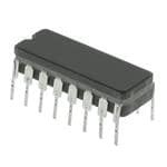
| 供应商器件封装 | 14-CDIP |
| 功能 | 热电偶放大器 |
| 包装 | 管件 |
| 商标 | Analog Devices |
| 安装类型 | 通孔 |
| 安装风格 | Through Hole |
| 封装 | Tube |
| 封装/外壳 | 14-CDIP(0.300",7.62mm) |
| 封装/箱体 | CDIP-14 |
| 工作温度 | -55°C ~ 125°C |
| 工作电源电压 | 5 V to +/- 15 V |
| 工厂包装数量 | 25 |
| 感应温度 | - |
| 拓扑 | 冰点补偿,过载检测 |
| 最大工作温度 | + 125 C |
| 最小工作温度 | - 55 C |
| 标准包装 | 25 |
| 电压-电源 | 5 V ~ ±15 V |
| 电源电流 | 300 uA |
| 精度 | ±3°C(最大) |
| 系列 | AD595 |
| 视频文件 | http://www.digikey.cn/classic/video.aspx?PlayerID=1364138032001&width=640&height=505&videoID=2245193158001 |
| 输出报警 | 是 |
| 输出格式 | Analog |
| 输出类型 | 电压 |
| 输出风扇 | 无 |


- 商务部:美国ITC正式对集成电路等产品启动337调查
- 曝三星4nm工艺存在良率问题 高通将骁龙8 Gen1或转产台积电
- 太阳诱电将投资9.5亿元在常州建新厂生产MLCC 预计2023年完工
- 英特尔发布欧洲新工厂建设计划 深化IDM 2.0 战略
- 台积电先进制程称霸业界 有大客户加持明年业绩稳了
- 达到5530亿美元!SIA预计今年全球半导体销售额将创下新高
- 英特尔拟将自动驾驶子公司Mobileye上市 估值或超500亿美元
- 三星加码芯片和SET,合并消费电子和移动部门,撤换高东真等 CEO
- 三星电子宣布重大人事变动 还合并消费电子和移动部门
- 海关总署:前11个月进口集成电路产品价值2.52万亿元 增长14.8%


PDF Datasheet 数据手册内容提取
a Monolithic Thermocouple Amplifiers with Cold Junction Compensation AD594/AD595 FEATURES FUNCTIONAL BLOCK DIAGRAM Pretrimmed for Type J (AD594) or Type K (AD595) Thermocouples –IN –ALM +ALM V+ COMP VO FB Can Be Used with Type T Thermocouple Inputs 14 13 12 11 10 9 8 Low Impedance Voltage Output: 10 mV/8C OVERLOAD Built-In Ice Point Compensation DETECT Wide Power Supply Range: +5 V to 615 V AD594/AD595 Low Power: <1 mW typical +A Thermocouple Failure Alarm Laser Wafer Trimmed to 18C Calibration Accuracy G G ICE Setpoint Mode Operation POINT COMP. –TC Self-Contained Celsius Thermometer Operation +TC High Impedance Differential Input Side-Brazed DIP or Low Cost Cerdip 1 2 3 4 5 6 7 +IN +C +T COM –T –C V– PRODUCT DESCRIPTION are available at the package pins so that the circuit can be The AD594/AD595 is a complete instrumentation amplifier and recalibrated for the thermocouple types by the addition of two thermocouple cold junction compensator on a monolithic chip. or three resistors. These terminals also allow more precise cali- It combines an ice point reference with a precalibrated amplifier bration for both thermocouple and thermometer applications. to produce a high level (10 mV/(cid:176) C) output directly from a ther- The AD594/AD595 is available in two performance grades. The mocouple signal. Pin-strapping options allow it to be used as a C and the A versions have calibration accuracies of – 1(cid:176) C and linear amplifier-compensator or as a switched output setpoint – 3(cid:176) C, respectively. Both are designed to be used from 0(cid:176) C to controller using either fixed or remote setpoint control. It can +50(cid:176) C, and are available in 14-pin, hermetically sealed, side- be used to amplify its compensation voltage directly, thereby brazed ceramic DIPs as well as low cost cerdip packages. converting it to a stand-alone Celsius transducer with a low impedance voltage output. PRODUCT HIGHLIGHTS The AD594/AD595 includes a thermocouple failure alarm that 1. The AD594/AD595 provides cold junction compensation, indicates if one or both thermocouple leads become open. The amplification, and an output buffer in a single IC package. alarm output has a flexible format which includes TTL drive 2. Compensation, zero, and scale factor are all precalibrated by capability. laser wafer trimming (LWT) of each IC chip. The AD594/AD595 can be powered from a single ended supply 3. Flexible pinout provides for operation as a setpoint control- (including +5 V) and by including a negative supply, tempera- ler or a stand-alone temperature transducer calibrated in tures below 0(cid:176) C can be measured. To minimize self-heating, an degrees Celsius. unloaded AD594/AD595 will typically operate with a total sup- ply current 160 m A, but is also capable of delivering in excess of 4. Operation at remote application sites is facilitated by low – 5 mA to a load. quiescent current and a wide supply voltage range +5 V to dual supplies spanning 30 V. The AD594 is precalibrated by laser wafer trimming to match 5. Differential input rejects common-mode noise voltage on the the characteristic of type J (iron-constantan) thermocouples and thermocouple leads. the AD595 is laser trimmed for type K (chromel-alumel) inputs. The temperature transducer voltages and gain control resistors REV.C Information furnished by Analog Devices is believed to be accurate and reliable. However, no responsibility is assumed by Analog Devices for its use, nor for any infringements of patents or other rights of third parties One Technology Way, P.O. Box 9106, Norwood, MA 02062-9106, U.S.A. which may result from its use. No license is granted by implication or Tel: 781/329-4700 World Wide Web Site: http://www.analog.com otherwise under any patent or patent rights of Analog Devices. Fax: 781/326-8703 © Analog Devices, Inc., 1999
AD594/AD595–SPECIFICATIONS (@ +258C and V = 5 V, Type J (AD594), Type K (AD595) Thermocouple, S unless otherwise noted) Model AD594A AD594C AD595A AD595C Min Typ Max Min Typ Max Min Typ Max Min Typ Max Units ABSOLUTE MAXIMUM RATING +VS to –VS 36 36 36 36 Volts Common-Mode Input Voltage –VS – 0.15 +VS –VS – 0.15 +VS –VS – 0.15 +VS –VS – 0.15 +VS Volts Differential Input Voltage –VS +VS –VS +VS –VS +VS –VS +VS Volts Alarm Voltages +ALM –VS –VS + 36 –VS –VS + 36 –VS –VS + 36 –VS –VS + 36 Volts –ALM –VS +VS –VS +VS –VS +VS –VS +VS Volts Operating Temperature Range –55 +125 –55 +125 –55 +125 –55 +125 (cid:176)C Output Short Circuit to Common Indefinite Indefinite Indefinite Indefinite TEMPERATURE MEASUREMENT (Specified Temperature Range 0(cid:176)C to +50(cid:176)C) Calibration Error at +25(cid:176)C1 63 61 63 61 (cid:176)C Stability vs. Temperature2 60.05 60.025 60.05 60.025 (cid:176)C/(cid:176)C Gain Error 61.5 60.75 61.5 60.75 % Nominal Transfer Function 10 10 10 10 mV/(cid:176)C AMPLIFIER CHARACTERISTICS Closed Loop Gain3 193.4 193.4 247.3 247.3 Input Offset Voltage (Temperature in (cid:176)C) · (Temperature in (cid:176)C) · (Temperature in (cid:176)C) · (Temperature in (cid:176)C) · 51.70 m V/(cid:176)C 51.70 m V/(cid:176)C 40.44 m V/(cid:176)C 40.44 m V/(cid:176)C m V Input Bias Current 0.1 0.1 0.1 0.1 m A Differential Input Range –10 +50 –10 +50 –10 +50 mV Common-Mode Range –VS – 0.15 –VS – 4 –VS – 0.15 –VS – 4 –VS – 0.15 –VS – 4 –VS – 0.15 –VS – 4 Volts Common-Mode Sensitivity – RTO 10 10 10 10 mV/V Power Supply Sensitivity – RTO 10 10 10 10 mV/V Output Voltage Range Dual Supply –VS + 2.5 +VS – 2 –VS + 2.5 +VS – 2 –VS + 2.5 +VS – 2 –VS + 2.5 +VS – 2 Volts Single Supply 0 +VS – 2 0 –VS – 2 0 +VS + 2 0 +VS – 2 Volts Usable Output Current4 – 5 – 5 – 5 – 5 mA 3 dB Bandwidth 15 15 15 15 kHz ALARM CHARACTERISTICS VCE(SAT) at 2 mA 0.3 0.3 0.3 0.3 Volts Leakage Current 61 61 61 61 m A max Operating Voltage at – ALM +VS – 4 +VS – 4 +VS – 4 +VS – 4 Volts Short Circuit Current 20 20 20 20 mA POWER REQUIREMENTS Specified Performance +VS = 5, –VS = 0 +VS = 5, –VS = 0 +VS = 5, –VS = 0 +VS = 5, –VS = 0 Volts Operating5 +VS to –VS £ 30 +VS to –VS £ 30 +VS to –VS £ 30 +VS to –VS £ 30 Volts Quiescent Current (No Load) +VS 160 300 160 300 160 300 160 300 m A –VS 100 100 100 100 m A PACKAGE OPTION TO-116 (D-14) AD594AD AD594CD AD595AD AD595CD Cerdip (Q-14) AD594AQ AD594CQ AD595AQ AD595CQ NOTES 1Calibrated for minimum error at +25(cid:176)C using a thermocouple sensitivity of 51.7 m V/(cid:176)C. Since a J type thermocouple deviates from this straight line approximation, the AD594 will normally read 3.1 mV when the measuring junction is at 0(cid:176)C. The AD595 will similarly read 2.7 mV at 0(cid:176)C. 2Defined as the slope of the line connecting the AD594/AD595 errors measured at 0(cid:176)C and 50(cid:176)C ambient temperature. 3Pin 8 shorted to Pin 9. 4Current Sink Capability in single supply configuration is limited to current drawn to ground through a 50 kW resistor at output voltages below 2.5 V. 5–VS must not exceed –16.5 V. Specifications shown in boldface are tested on all production units at final electrical test. Results from those tests are used to calculate outgoing quality levels. All min and max specifications are guaranteed, although only those shown in boldface are tested on all production units. Specifications subject to change without notice. INTERPRETING AD594/AD595 OUTPUT VOLTAGES compensated signal, the following transfer functions should be To achieve a temperature proportional output of 10 mV/(cid:176) C and used to determine the actual output voltages: accurately compensate for the reference junction over the rated AD594 output = (Type J Voltage + 16 m V) · 193.4 operating range of the circuit, the AD594/AD595 is gain trimmed AD595 output = (Type K Voltage + 11 m V) · 247.3 or conversely: to match the transfer characteristic of J and K type thermocouples Type J voltage = (AD594 output/193.4) – 16 m V at 25(cid:176) C. For a type J output in this temperature range the TC is 51.70 m V/(cid:176) C, while for a type K it is 40.44 m V/(cid:176) C. The resulting Type K voltage = (AD595 output/247.3) – 11 m V gain for the AD594 is 193.4 (10 mV/(cid:176) C divided by 51.7 m V/(cid:176) C) Table I lists the ideal AD594/AD595 output voltages as a func- and for the AD595 is 247.3 (10 mV/(cid:176) C divided by 40.44 m V/(cid:176) C). tion of Celsius temperature for type J and K ANSI standard In addition, an absolute accuracy trim induces an input offset to thermocouples, with the package and reference junction at the output amplifier characteristic of 16 m V for the AD594 and 25(cid:176) C. As is normally the case, these outputs are subject to cali- 11 m V for the AD595. This offset arises because the AD594/ bration, gain and temperature sensitivity errors. Output values AD595 is trimmed for a 250 mV output while applying a 25(cid:176) C for intermediate temperatures can be interpolated, or calculated thermocouple input. using the output equations and ANSI thermocouple voltage tables referred to zero degrees Celsius. Due to a slight variation Because a thermocouple output voltage is nonlinear with respect to temperature, and the AD594/AD595 linearly amplifies the in alloy content between ANSI type J and DIN FE-CUNI –2– REV. C
AD594/AD595 Table I. Output Voltage vs. Thermocouple Temperature (Ambient +25(cid:176) C, V = –5 V, +15 V) S Thermocouple Type J AD594 Type K AD595 Thermocouple Type J AD594 Type K AD595 Temperature Voltage Output Voltage Output Temperature Voltage Output Voltage Output (cid:176)C mV mV mV mV (cid:176)C mV mV mV mV –200 –7.890 –1523 –5.891 –1454 500 27.388 5300 20.640 5107 –180 –7.402 –1428 –5.550 –1370 520 28.511 5517 21.493 5318 –160 –6.821 –1316 –5.141 –1269 540 29.642 5736 22.346 5529 –140 –6.159 –1188 –4.669 –1152 560 30.782 5956 23.198 5740 –120 –5.426 –1046 –4.138 –1021 580 31.933 6179 24.050 5950 –100 –4.632 –893 –3.553 –876 600 33.096 6404 24.902 6161 –80 –3.785 –729 –2.920 –719 620 34.273 6632 25.751 6371 –60 –2.892 –556 –2.243 –552 640 35.464 6862 26.599 6581 –40 –1.960 –376 –1.527 –375 660 36.671 7095 27.445 6790 –20 –.995 –189 –.777 –189 680 37.893 7332 28.288 6998 –10 –.501 –94 –.392 –94 700 39.130 7571 29.128 7206 0 0 3.1 0 2.7 720 40.382 7813 29.965 7413 10 .507 101 .397 101 740 41.647 8058 30.799 7619 20 1.019 200 .798 200 750 42.283 8181 31.214 7722 25 1.277 250 1.000 250 760 – – 31.629 7825 30 1.536 300 1.203 300 780 – – 32.455 8029 40 2.058 401 1.611 401 800 – – 33.277 8232 50 2.585 503 2.022 503 820 – – 34.095 8434 60 3.115 606 2.436 605 840 – – 34.909 8636 80 4.186 813 3.266 810 860 – – 35.718 8836 100 5.268 1022 4.095 1015 880 – – 36.524 9035 120 6.359 1233 4.919 1219 900 – – 37.325 9233 140 7.457 1445 5.733 1420 920 – – 38.122 9430 160 8.560 1659 6.539 1620 940 – – 38.915 9626 180 9.667 1873 7.338 1817 960 – – 39.703 9821 200 10.777 2087 8.137 2015 980 – – 40.488 10015 220 11.887 2302 8.938 2213 1000 – – 41.269 10209 240 12.998 2517 9.745 2413 1020 – – 42.045 10400 260 14.108 2732 10.560 2614 1040 – – 42.817 10591 280 15.217 2946 11.381 2817 1060 – – 43.585 10781 300 16.325 3160 12.207 3022 1080 – – 44.439 10970 320 17.432 3374 13.039 3227 1100 – – 45.108 11158 340 18.537 3588 13.874 3434 1120 – – 45.863 11345 360 19.640 3801 14.712 3641 1140 – – 46.612 11530 380 20.743 4015 15.552 3849 1160 – – 47.356 11714 400 21.846 4228 16.395 4057 1180 – – 48.095 11897 420 22.949 4441 17.241 4266 1200 – – 48.828 12078 440 24.054 4655 18.088 4476 1220 – – 49.555 12258 460 25.161 4869 18.938 4686 1240 – – 50.276 12436 480 26.272 5084 19.788 4896 1250 – – 50.633 12524 thermocouples Table I should not be used in conjunction with SINGLE AND DUAL SUPPLY CONNECTIONS European standard thermocouples. Instead the transfer function The AD594/AD595 is a completely self-contained thermocouple given previously and a DIN thermocouple table should be used. conditioner. Using a single +5 V supply the interconnections ANSI type K and DIN NICR-NI thermocouples are composed shown in Figure 1 will provide a direct output from a type J thermocouple (AD594) or type K thermocouple (AD595) mea- C(AOLNUSMTEALN)TAN +5V 10mV/8C suring from 0(cid:176) C to +300(cid:176) C. Any convenient supply voltage from +5 V to +30 V may be 14 13 12 11 10 9 8 used, with self-heating errors being minimized at lower supply OVERLOAD DETECT levels. In the single supply configuration the +5 V supply con- AD594/ AD595 +A nects to Pin 11 with the V– connection at Pin 7 strapped to power and signal common at Pin 4. The thermocouple wire in- G G ICE POINT puts connect to Pins 1 and 14 either directly from the measuring +TC COMP.–TC point or through intervening connections of similar thermo- IRON (CHROMEL) 1 2 3 4 5 6 7 couple wire type. When the alarm output at Pin 13 is not used it COMMON should be connected to common or –V. The precalibrated feed- back network at Pin 8 is tied to the output at Pin 9 to provide a Figure 1.Basic Connection, Single Supply Operation 10 mV/(cid:176) C nominal temperature transfer characteristic. of identical alloys and exhibit similar behavior. The upper tem- By using a wider ranging dual supply, as shown in Figure 2, the perature limits in Table I are those recommended for type J and AD594/AD595 can be interfaced to thermocouples measuring type K thermocouples by the majority of vendors. both negative and extended positive temperatures. REV. C –3–
AD594/AD595 +5V TO +30V The printed circuit board layout shown also provides for place- CONSTANTAN (ALUMEL) ment of optional alarm load resistors, recalibration resistors and a compensation capacitor to limit bandwidth. 14 13 12 11 10 9 8 ODEVTEERCLTOAD To ensure secure bonding the thermocouple wire should be AD594/ cleaned to remove oxidation prior to soldering. Noncorrosive AD595 +A SPAN OF rosin flux is effective with iron, constantan, chromel and alumel 5V TO 30V G G ICE and the following solders: 95% tin-5% antimony, 95% tin-5% POINT–TC +TC COMP. silver or 90% tin-10% lead. IRON 1 2 3 4 5 6 7 (CHROMEL) FUNCTIONAL DESCRIPTION COMMON The AD594 behaves like two differential amplifiers. The out- puts are summed and used to control a high gain amplifier, as 0V TO –25V shown in Figure 4. Figure 2.Dual Supply Operation With a negative supply the output can indicate negative tem- –IN –ALM +ALM V+ COMP VO FB peratures and drive grounded loads or loads returned to positive 14 13 12 11 10 9 8 voltages. Increasing the positive supply from 5 V to 15 V ex- OVERLOAD tends the output voltage range well beyond the 750(cid:176) C DETECT temperature limit recommended for type J thermocouples AD594/AD595 (AD594) and the 1250(cid:176) C for type K thermocouples (AD595). +A Common-mode voltages on the thermocouple inputs must remain within the common-mode range of the AD594/AD595, with a G G ICE POINT return path provided for the bias currents. If the thermocouple COMP. –TC +TC is not remotely grounded, then the dotted line connections in Figures 1 and 2 are recommended. A resistor may be needed in 1 2 3 4 5 6 7 this connection to assure that common-mode voltages induced +IN +C +T COM –T –C V– in the thermocouple loop are not converted to normal mode. Figure 4.AD594/AD595 Block Diagram THERMOCOUPLE CONNECTIONS In normal operation the main amplifier output, at Pin 9, is con- The isothermal terminating connections of a pair of thermo- nected to the feedback network, at Pin 8. Thermocouple signals couple wires forms an effective reference junction. This junction applied to the floating input stage, at Pins 1 and 14, are ampli- must be kept at the same temperature as the AD594/AD595 for fied by gain G of the differential amplifier and are then further the internal cold junction compensation to be effective. amplified by gain A in the main amplifier. The output of the A method that provides for thermal equilibrium is the printed main amplifier is fed back to a second differential stage in an in- circuit board connection layout illustrated in Figure 3. verting connection. The feedback signal is amplified by this stage and is also applied to the main amplifier input through a summing circuit. Because of the inversion, the amplifier causes IRON CONSTANTAN the feedback to be driven to reduce this difference signal to a (CHROMEL) (ALUMEL) small value. The two differential amplifiers are made to match and have identical gains, G. As a result, the feedback signal that +T +C must be applied to the right-hand differential amplifier will pre- cisely match the thermocouple input signal when the difference +IN –IN signal has been reduced to zero. The feedback network is trim- 1 14 +ALM med so that the effective gain to the output, at Pins 8 and 9, re- –ALM sults in a voltage of 10 mV/(cid:176) C of thermocouple excitation. In addition to the feedback signal, a cold junction compensation voltage is applied to the right-hand differential amplifier. The compensation is a differential voltage proportional to the Celsius temperature of the AD594/AD595. This signal disturbs the dif- COMP 7 8 ferential input so that the amplifier output must adjust to restore the input to equal the applied thermocouple voltage. The compensation is applied through the gain scaling resistors COMMON –T –C V– VOUT V+ so that its effect on the main output is also 10 mV/(cid:176) C. As a Figure 3.PCB Connections result, the compensation voltage adds to the effect of the ther- mocouple voltage a signal directly proportional to the difference Here the AD594/AD595 package temperature and circuit board between 0(cid:176) C and the AD594/AD595 temperature. If the thermo- are thermally contacted in the copper printed circuit board couple reference junction is maintained at the AD594/AD595 tracks under Pins 1 and 14. The reference junction is now com- temperature, the output of the AD594/AD595 will correspond posed of a copper-constantan (or copper-alumel) connection to the reading that would have been obtained from amplification and copper-iron (or copper-chromel) connection, both of which of a signal from a thermocouple referenced to an ice bath. are at the same temperature as the AD594/AD595. –4– REV. C
AD594/AD595 The AD594/AD595 also includes an input open circuit detector this terminal can be produced with a resistor between –C and that switches on an alarm transistor. This transistor is actually a –T to balance an increase in +T, or a resistor from –T to COM current-limited output buffer, but can be used up to the limit as to offset a decrease in +T. a switch transistor for either pull-up or pull-down operation of If the compensation is adjusted substantially to accommodate a external alarms. different thermocouple type, its effect on the final output volt- The ice point compensation network has voltages available with age will increase or decrease in proportion. To restore the positive and negative temperature coefficients. These voltages nominal output to 10 mV/(cid:176) C the gain may be adjusted to match may be used with external resistors to modify the ice point com- the new compensation and thermocouple input characteristics. pensation and recalibrate the AD594/AD595 as described in the When reducing the compensation the resistance between –T next column. and COM automatically increases the gain to within 0.5% of the correct value. If a smaller gain is required, however, the nominal The feedback resistor is separately pinned out so that its value 47 kW internal feedback resistor can be paralleled or replaced can be padded with a series resistor, or replaced with an external with an external resistor. resistor between Pins 5 and 9. External availability of the feedback resistor allows gain to be adjusted, and also permits the AD594/ Fine calibration adjustments will require temperature response AD595 to operate in a switching mode for setpoint operation. measurements of individual devices to assure accuracy. Major reconfigurations for other thermocouple types can be achieved CAUTIONS: without seriously compromising initial calibration accuracy, so The temperature compensation terminals (+C and –C) at Pins 2 long as the procedure is done at a fixed temperature using the and 6 are provided to supply small calibration currents only. The factory calibration as a reference. It should be noted that inter- AD594/AD595 may be permanently damaged if they are mediate recalibration conditions may require the use of a grounded or connected to a low impedance. negative supply. The AD594/AD595 is internally frequency compensated for feed- EXAMPLE: TYPE E RECALIBRATION—AD594/AD595 back ratios (corresponding to normal signal gain) of 75 or more. Both the AD594 and AD595 can be configured to condition the If a lower gain is desired, additional frequency compensation output of a type E (chromel-constantan) thermocouple. Tem- should be added in the form of a 300 pF capacitor from Pin 10 perature characteristics of type E thermocouples differ less from to the output at Pin 9. As shown in Figure 5 an additional 0.01 m F type J, than from type K, therefore the AD594 is preferred for capacitor between Pins 10 and 11 is recommended. recalibration. While maintaining the device at a constant temperature follow AD594/ VO 9 the recalibration steps given here. First, measure the device AD595 300pF temperature by tying both inputs to common (or a selected COMP 10 0.01mF common-mode potential) and connecting FB to VO. The AD594 +V 11 is now in the stand alone Celsius thermometer mode. For this example assume the ambient is 24(cid:176) C and the initial output VO Figure 5.Low Gain Frequency Compensation is 240 mV. Check the output at VO to verify that it corresponds RECALIBRATION PRINCIPLES AND LIMITATIONS to the temperature of the device. The ice point compensation network of the AD594/AD595 Next, measure the voltage –T at Pin 5 with a high impedance produces a differential signal which is zero at 0(cid:176) C and corre- DVM (capacitance should be isolated by a few thousand ohms sponds to the output of an ice referenced thermocouple at the of resistance at the measured terminals). At 24(cid:176) C the –T voltage temperature of the chip. The positive TC output of the circuit is will be about 8.3 mV. To adjust the compensation of an AD594 proportional to Kelvin temperature and appears as a voltage at to a type E thermocouple a resistor, R1, should be connected +T. It is possible to decrease this signal by loading it with a between +T and +C, Pins 2 and 3, to raise the voltage at –T by resistor from +T to COM, or increase it with a pull-up resistor the ratio of thermocouple sensitivities. The ratio for converting a from +T to the larger positive TC voltage at +C. Note that type J device to a type E characteristic is: adjustments to +T should be made by measuring the voltage which r (AD594) =(60.9 m V/(cid:176) C)/(51.7 m V/(cid:176) C)= 1.18 tracks it at –T. To avoid destabilizing the feedback amplifier the measuring instrument should be isolated by a few thousand Thus, multiply the initial voltage measured at –T by r and ex- ohms in series with the lead connected to –T. perimentally determine the R1 value required to raise –T to that level. For the example the new –T voltage should be about 9.8 mV. The resistance value should be approximately 1.8 kW . 1 +IN AD594/ +T 3 The zero differential point must now be shifted back to 0(cid:176) C. 14 –IN AD595 This is accomplished by multiplying the original output voltage COM 4 VO by r and adjusting the measured output voltage to this value 8 FB by experimentally adding a resistor, R2, between –C and –T, 9 VO –T 5 Pins 5 and 6. The target output value in this case should be about 283 mV. The resistance value of R2 should be approxi- Figure 6. Decreased Sensitivity Adjustment mately 240 kW . Changing the positive TC half of the differential output of the Finally, the gain must be recalibrated such that the output VO compensation scheme shifts the zero point away from 0(cid:176) C. The indicates the device’s temperature once again. Do this by adding zero can be restored by adjusting the current flow into the nega- a third resistor, R3, between FB and –T, Pins 8 and 5. VO should tive input of the feedback amplifier, the –T pin. A current into now be back to the initial 240 mV reading. The resistance value REV. C –5–
AD594/AD595 of R3 should be approximately 280 kW . The final connection THERMAL ENVIRONMENT EFFECTS diagram is shown in Figure 7. An approximate verification of The inherent low power dissipation of the AD594/AD595 and the effectiveness of recalibration is to measure the differential the low thermal resistance of the package make self-heating gain to the output. For type E it should be 164.2. errors almost negligible. For example, in still air the chip to am- bient thermal resistance is about 80(cid:176) C/watt (for the D package). At the nominal dissipation of 800 m W the self-heating in free air is less than 0.065(cid:176) C. Submerged in fluorinert liquid (unstirred) 1 +IN COM 4 the thermal resistance is about 40(cid:176) C/watt, resulting in a self- 14 –IN +T 3 heating error of about 0.032(cid:176) C. AD594/ R1 AD595 +C 2 SETPOINT CONTROLLER The AD594/AD595 can readily be connected as a setpoint –C 6 9 VO R2 controller as shown in Figure 9. 8 FB –T 5 HEATER LOW = > T < SETPOINT DRIVER TEMPERATURE HIGH = > T > SETPOINT R3 COMPARATOR OUT CONSTANTAN SETPOINT Figure 7.Type E Recalibration HEATER (ALUMEL) +5V VOLTAGE INPUT When implementing a similar recalibration procedure for the 14 13 12 11 10 9 8 AD595 the values for R1, R2, R3 and r will be approximately OVERLOAD 20MV DETECT (OPTIONAL) 650 W , 84 kW , 93 kW and 1.51, respectively. Power consump- AD594/ FOR tion will increase by about 50% when using the AD595 with AD595 +A HYSTERESIS type E inputs. G G ICE POINT–TC Note that during this procedure it is crucial to maintain the +TC COMP. IRON AD594/AD595 at a stable temperature because it is used as the (CHROMEL) 1 2 3 4 5 6 7 temperature reference. Contact with fingers or any tools not at TEMPERATURE COMMON ambient temperature will quickly produce errors. Radiational CONTROLLED REGION heating from a change in lighting or approach of a soldering iron must also be guarded against. Figure 9. Setpoint Controller The thermocouple is used to sense the unknown temperature USING TYPE T THERMOCOUPLES WITH THE AD595 and provide a thermal EMF to the input of the AD594/AD595. Because of the similarity of thermal EMFs in the 0(cid:176) C to +50(cid:176) C The signal is cold junction compensated, amplified to 10 mV/(cid:176) C range between type K and type T thermocouples, the AD595 and compared to an external setpoint voltage applied by the can be directly used with both types of inputs. Within this ambi- user to the feedback at Pin 8. Table I lists the correspondence ent temperature range the AD595 should exhibit no more than between setpoint voltage and temperature, accounting for the an additional 0.2(cid:176) C output calibration error when used with nonlinearity of the measurement thermocouple. If the setpoint type T inputs. The error arises because the ice point compensa- temperature range is within the operating range (–55(cid:176) C to tor is trimmed to type K characteristics at 25(cid:176) C. To calculate +125(cid:176) C) of the AD594/AD595, the chip can be used as the the AD595 output values over the recommended –200(cid:176) C to transducer for the circuit by shorting the inputs together and +350(cid:176) C range for type T thermocouples, simply use the ANSI utilizing the nominal calibration of 10 mV/(cid:176) C. This is the centi- thermocouple voltages referred to 0(cid:176) C and the output equation grade thermometer configuration as shown in Figure 13. given on page 2 for the AD595. Because of the relatively large nonlinearities associated with type T thermocouples the output In operation if the setpoint voltage is above the voltage corre- will deviate widely from the nominal 10 mV/(cid:176) C. However, cold sponding to the temperature being measured the output swings junction compensation over the rated 0(cid:176) C to +50(cid:176) C ambient low to approximately zero volts. Conversely, when the tempera- will remain accurate. ture rises above the setpoint voltage the output switches to the positive limit of about 4 volts with a +5 V supply. Figure STABILITY OVER TEMPERATURE 9 shows the setpoint comparator configuration complete with a Each AD594/AD595 is tested for error over temperature with heater element driver circuit being controlled by the AD594/ the measuring thermocouple at 0(cid:176) C. The combined effects of AD595 toggled output. Hysteresis can be introduced by inject- cold junction compensation error, amplifier offset drift and gain ing a current into the positive input of the feedback amplifier error determine the stability of the AD594/AD595 output over when the output is toggled high. With an AD594 about 200 nA the rated ambient temperature range. Figure 8 shows an AD594/ into the +T terminal provides 1(cid:176) C of hysteresis. When using a AD595 drift error envelope. The slope of this figure has units single 5 V supply with an AD594, a 20 MW resistor from V to of (cid:176) C/(cid:176) C. O +T will supply the 200 nA of current when the output is forced high (about 4 V). To widen the hysteresis band decrease the +0.68C resistance connected from VO to +T. R O R ER 0 FT 258C 508C RI D –0.68C TEMPERATURE OF AD594C/AD595C Figure 8.Drift Error vs. Temperature –6– REV. C
AD594/AD595 ALARM CIRCUIT The alarm can be used with both single and dual supplies. It In all applications of the AD594/AD595 the –ALM connection, can be operated above or below ground. The collector and emit- Pin 13, should be constrained so that it is not more positive ter of the output transistor can be used in any normal switch than (V+) – 4 V. This can be most easily achieved by connect- configuration. As an example a negative referenced load can be ing Pin 13 to either common at Pin 4 or V– at Pin 7. For most driven from –ALM as shown in Figure 12. applications that use the alarm signal, Pin 13 will be grounded and the signal will be taken from +ALM on Pin 12. A typical +10V CONSTANTAN application is shown in Figure 10. (ALUMEL) In this configuration the alarm transistor will be off in normal 14 13 12 11 10 9 8 10mV/8C operation and the 20 k pull up will cause the +ALM output on ODEVTEERCLTOAD Pin 12 to go high. If one or both of the thermocouple leads are AD594/ AD595 +A interrupted, the +ALM pin will be driven low. As shown in Fig- ure 10 this signal is compatible with the input of a TTL gate G G ICE POINT–TC which can be used as a buffer and/or inverter. +TC COMP. IRON 1 2 3 4 5 6 7 (CHROMEL) +5V GND 20kV ALARM CONSTANTAN ALARM OUT TTL GATE (ALUMEL) ALARM 14 13 12 11 10 9 8 10mV/8C RELAY –12V OVERLOAD DETECT AD594/ Figure 12.–ALM Driving A Negative Referenced Load AD595 +A The collector (+ALM) should not be allowed to become more G G ICE POINT–TC positive than (V–) +36 V, however, it may be permitted to be +TC COMP. more positive than V+. The emitter voltage (–ALM) should be IRON (CHROMEL) 1 2 3 4 5 6 7 constrained so that it does not become more positive than 4 volts below the V+ applied to the circuit. GND Additionally, the AD594/AD595 can be configured to produce Figure 10. Using the Alarm to Drive a TTL Gate an extreme upscale or downscale output in applications where (“Grounded’’ Emitter Configuration) an extra signal line for an alarm is inappropriate. By tying either Since the alarm is a high level output it may be used to directly of the thermocouple inputs to common most runaway control drive an LED or other indicator as shown in Figure 11. conditions can be automatically avoided. A +IN to common connection creates a downscale output if the thermocouple opens, V+ while connecting –IN to common provides an upscale output. LED CELSIUS THERMOMETER CONSTANTAN 270V The AD594/AD595 may be configured as a stand-alone Celsius (ALUMEL) 10mV/8C thermometer as shown in Figure 13. 14 13 12 11 10 9 8 OVERLOAD DETECT +5V TO +15V AD594/ AD595 +A 14 13 12 11 10 9 8 O10UmTVP/U8CT G G POICIENT–TC ODEVTEERCLTOAD +TC COMP. AD594/ AD595 +A IRON (CHROMEL) 1 2 3 4 5 6 7 G G ICE COMMON POINT–TC +TC COMP. Figure 11.Alarm Directly Drives LED 1 2 3 4 5 6 7 A 270 W series resistor will limit current in the LED to 10 mA, GND but may be omitted since the alarm output transistor is current 0 TO –15V limited at about 20 mA. The transistor, however, will operate in Figure 13.AD594/AD595 as a Stand-Alone Celsius a high dissipation mode and the temperature of the circuit will Thermometer rise well above ambient. Note that the cold junction compensa- Simply omit the thermocouple and connect the inputs (Pins 1 tion will be affected whenever the alarm circuit is activated. The and 14) to common. The output now will reflect the compensa- time required for the chip to return to ambient temperature will tion voltage and hence will indicate the AD594/AD595 depend on the power dissipation of the alarm circuit, the nature temperature with a scale factor of 10 mV/(cid:176) C. In this three termi- of the thermal path to the environment and the alarm duration. nal, voltage output, temperature sensing mode, the AD594/ AD595 will operate over the full military –55(cid:176) C to +125(cid:176) C tem- perature range. REV. C –7–
AD594/AD595 THERMOCOUPLE BASICS and to arrange its output voltage so that it corresponds to a ther- Thermocouples are economical and rugged; they have reason- mocouple referred to 0(cid:176) C. This voltage is simply added to the ably good long-term stability. Because of their small size, they thermocouple voltage and the sum then corresponds to the stan- respond quickly and are good choices where fast response is im- dard voltage tabulated for an ice-point referenced thermocouple. portant. They function over temperature ranges from cryogenics to jet-engine exhaust and have reasonable linearity and accuracy. Because the number of free electrons in a piece of metal de- V1' V1 VFSO1C' RA= L PVER1DO VP3E' R=L fY(T3) 99 pends on both temperature and composition of the metal, two 1/ 1 pieces of dissimilar metal in isothermal and contact will exhibit – 0 a potential difference that is a repeatable function of tempera- CONSTANTANCu V2 CuCuNi– 1g– ture, as shown in Figure 14. The resulting voltage depends on 73 T3 V3' C the temperatures, T1 and T2, in a repeatable way. T1 V1 IRON Cu Cu Figure 15.Substitution of Measured Reference CONSTANTAN CONSTANTAN Temperature for Ice Point Reference T1 T2 The temperature sensitivity of silicon integrated circuit transis- IRON tors is quite predictable and repeatable. This sensitivity is UNKNOWN ICE POINT exploited in the AD594/AD595 to produce a temperature re- TEMPERATURE REFERENCE lated voltage to compensate the reference of “cold” junction of a Figure 14.Thermocouple Voltage with 0(cid:176) C Reference thermocouple as shown in Figure 16. Since the thermocouple is basically a differential rather than absolute measuring device, a know reference temperature is required for one of the junctions if the temperature of the other is to be inferred from the output voltage. Thermocouples made of specially selected materials have been exhaustively character- T3 ized in terms of voltage versus temperature compared to primary CONSTANTAN temperature standards. Most notably the water-ice point of 0(cid:176) C is used for tables of standard thermocouple performance. T1 Cu An alternative measurement technique, illustrated in Figure 15, is used in most practical applications where accuracy requirements IRON Cu do not warrant maintenance of primary standards. The reference junction temperature is allowed to change with the environment Figure 16.Connecting Isothermal Junctions of the measurement system, but it is carefully measured by some type of absolute thermometer. A measurement of the thermo- Since the compensation is at the reference junction temperature, couple voltage combined with a knowledge of the reference it is often convenient to form the reference “junction” by connect- temperature can be used to calculate the measurement junction ing directly to the circuit wiring. So long as these connections temperature. Usual practice, however, is to use a convenient and the compensation are at the same temperature no error will thermoelectric method to measure the reference temperature result. OUTLINE DIMENSIONS Dimensions shown in inches and (mm). TO-116 (D) Package Cerdip (Q) Package A. S. U. 0.430 (10.92) 0.77 – 0.015 N 14 8 (19.55 – 0.39) D I (1.00.20)4 R0 0(6.2.7635) 0(7.2.3970 ––00..2051)0 0.310 14 8 0.260 – 0.020 NTE 1 7 (7.87) (6.6 – 0.51) RI 1 7 P 0.300 (7.62) 0.035 – 0.010 PIN(01. 7710.708 – –00.0.2150) (07..3817 –– 00..2051) PIN 1 0(0.0.83859 – –00.0.21504) REF 0.148 – 0.015 (0.89 – 0.25) (3.76 – 0.38) 0.085 (2.16) 0.095 (2.41) 0.125 0.180 – 0.030 (03.M.112I8N5)0(1.0.1497 –– 00..1080)7 0.017+–00..000023 (02.1.5040) 0(4.1.5870 ––00..7063)00.30 (7.62) REF0(0.0.215 – –00.0.0052) 3(.01M0.78.I05N13)22) 0.60(000.. 04(115587.)24) 0(2.1.5040)SP(4EL.A5A7NT I–EN0G.76) 105(cid:176)(cid:176) 0(0.0.21504 – –00.0.00215) (0.43+0.08( BSC BSC BSC –0.05 –8– REV. C
Mouser Electronics Authorized Distributor Click to View Pricing, Inventory, Delivery & Lifecycle Information: A nalog Devices Inc.: AD594ADZ AD594AQ AD594CDZ AD594CQ AD595ADZ AD595AQ AD595CDZ AD595CQ